5.16. CDD PWM Module
5.16.1. Acronyms and Definitions
Abbreviation/Term |
Explanation |
|---|---|
AUTOSAR |
Automotive Open System Architecture |
CDD |
Complex Device Driver |
MCAL |
Micro Controller Abstraction Layer |
API |
Application Programming Interface |
DET |
Default Error Tracer |
HW |
Hardware |
SW |
Software |
LA |
Logic Analyzer |
EPWM |
Enhanced Pulse Width Modulation |
HRPWM |
High resolution PWM |
PWM Instance |
Single EPWM hardware unit |
Channel |
Each PWM instance supports two output channels EPWMxA and EPWMxB. Each output is considered as a channel |
PWM Output State |
Defines the output state for a PWM signal. It could be: High or Low |
PWM Idle State |
The idle state represents the output state of the PWM channel after the call of Cdd_Pwm_SetOutputToIdle or Cdd_Pwm_DeInit |
PWM Polarity |
Defines the starting output state of each PWM channel |
PWM Duty cycle |
Defines a percentage of the polarity(level) related to the period for each PWM channel |
PWM period |
Defines the value corresponds to the period of the PWM instance (This value is written into the TBPRD register). This is parameter is only applicable to the EPWM instance (not applicable to channel) |
TBPRD |
Time-Base Period -Period value that is written into the register |
SYSCLK |
System clock |
EPWMCLK |
Clock to the EPWM module |
EPWMCLKDIV |
EPWM clock divider. This divides the SYSCLK and produces EPWMCLK to the EPWM instances |
CLKDIV |
Clock divider prescaler which divides the EPWMCLK that is fed to the EPWM instance |
HSCLKDIV |
High speed clock divider, it is multiplied with CLKDIV and divides the EPWMCLK that is fed to the EPWM instance |
T_TBCLK |
Time period of the time-base clock. This is calculated based on the clock to the EPWM module and the configured clock prescalers. |
F_TBCLK |
Frequency of the time-base clock.(1/T_TBCLK) |
T_PWM |
Time Period of the generated PWM waveform |
F_PWM |
Frequency of the time-base clock.(1/T_PWM) |
GPIO |
General Purpose Input Output |
Edge |
Change in the output level from HIGH to LOW or LOW to HIGH |
5.16.2. Introduction
CDD PWM driver is a Complex Device Driver used to represent an analog signal with a digital approximation. It provides services to change the duty cycle and period of the PWM/EPWM channels. It provides service to set the PWM channels in the IDLE state. Furthermore, it provides services to enable and disable notification mechanism and routines to count the edges detected.
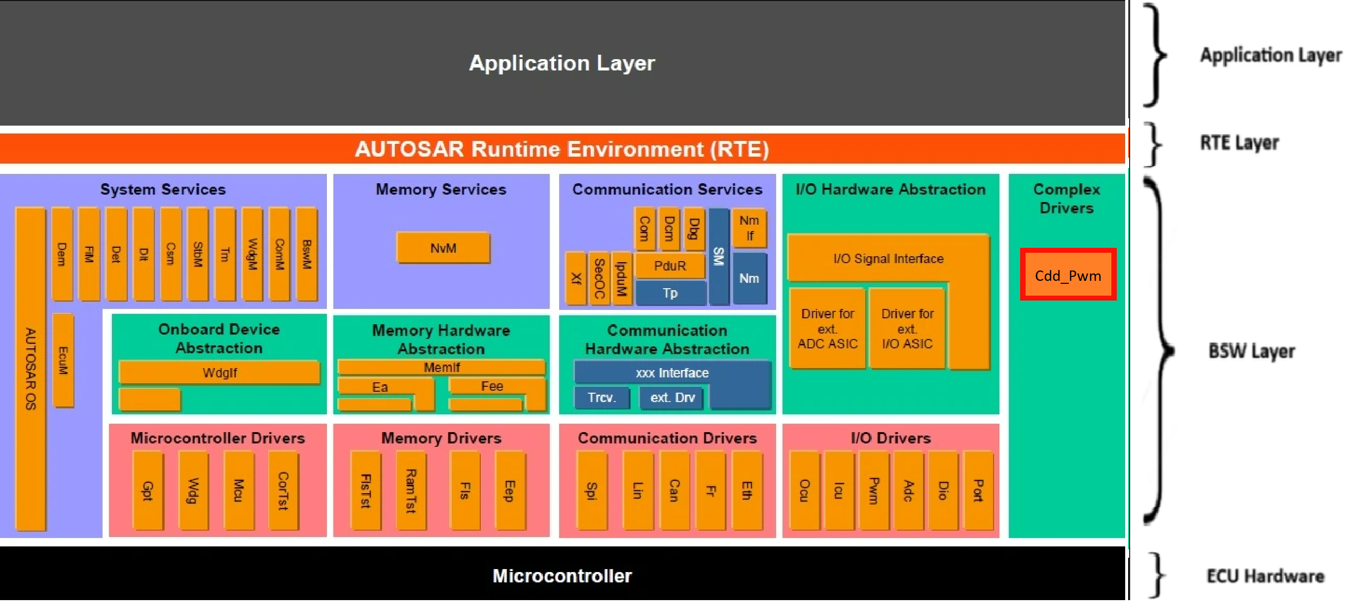
Fig. 5.62 Cdd Pwm MCAL AUTOSAR
This document details AUTOSAR Cdd Pwm module implementation
Supported AUTOSAR Release |
4.3.1 |
|---|---|
Supported Configuration Variants |
Pre-Compile |
Vendor ID |
CDD_PWM_VENDOR_ID (44) |
Module ID |
CDD_PWM_MODULE_ID (255) |
5.16.3. Functional Overview
EPWM (Enhanced Pulse width modulation)/PWM is a general method for representing an analog signal with a digital approximation. A PWM signal consists of a sequence of variable width, constant amplitude pulses which contain the same total energy as the original analog signal. This property is valuable in digital motor control as sinusoidal current (energy) can be delivered to the motor using PWM signals applied to a power converter.
The EPWM module supports two operational modes:
Simple Mode: Provides basic PWM functionality with standard features like duty cycle and period control. This mode is suitable for applications requiring basic PWM generation without advanced features.
Advanced Mode: This mode supports additional features such as trip zone functionality, dead-band generation, chopper functionality, digital compare, event trigger,diode emulation and other advanced capabilities. Advanced mode configuration can be done using APIs only. This mode is ideal for complex motor control applications, power conversion systems, and scenarios requiring precise timing control or fault protection.
It’s important to note that only one mode (either Simple or Advanced) can be used. The mode selection can be configured in the EB tresos configuration tool during the configuration phase. The selection determines which features will be available and affects the initialization parameters and available APIs.
Each EPWM instance supports 2 channels: Channel A & Channel B. Period and notification configuration is common for both the channels of the EPWM instance. Duty cycle can be configured independently.
5.16.3.1. Simple mode
5.16.3.1.1. APIs supported
Cdd_Pwm_Init -Start all PWM channels
Cdd_Pwm_DeInit -Stop all PWM channels
Cdd_Pwm_SetDutyCycle -Set the requested duty cycle for the PWM channel
Cdd_Pwm_SetPeriod -Set the requested period for the PWM instance
Cdd_Pwm_SetOutputToIdle -Set the output of the channel to the configured IDLE state
Cdd_Pwm_SetInterruptEventCount -Set the interrupt event prescale count for the instance, this should be called before enable notification API else a runtime error will be reported
Cdd_Pwm_EnableNotification -Enable interrupt for the channel. Notification function is common for both the channels of an EPWM instance
Cdd_Pwm_DisableNotification -Disable interrupt for the channel. Notification function is common for both the channels of an EPWM instance
Cdd_Pwm_GetVersionInfo -Retrieve software version information of the module
5.16.3.1.2. How the dutycycle is configured in the hardware in simple mode
In simple mode each EPWM uses 3 sub-modules that determines the output of the PWM channel, the sub-modules are:
5.16.3.1.2.1. Time Base counter
This sub-module primarily consists of a 16-bit counter which partially determines the period & frequency of the PWM waveform.
The mode of the time-base counter decides the symmetry of the waveform. For Asymmetric waveform the counter runs in Up-Count Mode and runs in Up-Down-Count Mode for symmetric waveforms.
Up-count Mode: The counter starts counting from zero and increments until it reaches the time-base period register value, then the counter resets to zero and the count sequence starts again.
Up-Down-Count Mode: The counter starts counting from zero and increments until it reaches the time-base period register value, then the counter decrements until it reaches zero and the count sequence repeats.
Clocking: The clock used for the EPWM counter is originally sourced from a device’s system clock. A configurable clock divider divides down the system clock to generate the EPWM clock (EPWMCLK). EPWM clock pre-scaler values can then be used to further divide down the EPWM clock for the EPWM counter and a EPWM time-base period register. The counter and the time-base period value control the frequency and period of the generated EPWM waveforms.
Time-Base Clock TBCLK = EPWMCLK / (HSPCLKDIV * CLKDIV) \
Clock Pre-scaler = HSPCLKDIV * CLKDIV
TBPRD = Period value from the configurator/with Cdd_Pwm_Period API
DutyCycle = DutyCycle value from the configurator/with Cdd_Pwm_SetDutyCycle API
Note
Shadow registers act like a buffer to allow register updates to be synchronized with the EPWM counter or a specific (configurable) event and avoid corruption or spurious operation from the register being modified asynchronously by software.
5.16.3.1.2.2. Counter Compare
When a match occurs (counter = CMPA / CMPB), this is known as a compare event. Compare events are used by the EPWM action-qualifier submodule to influence EPWM outputs.
An integral compare value is calculated based on the configured duty cycle of the channel and period of the instance. The output level can be decided based on the Action qualifier events. In scenarios where the calculated value is same for different configured duty cycles the output is going to be exactly same. Note that for up-count modes, a counter-compare match (counter = CMPx) can occur only once per cycle which produces a Asymmetric waveform; however, for up-down-count mode, a counter match can occur twice per cycle since there can be a match on the up-count and another match on the down-count which generates a Symmetric output waveform.
5.16.3.1.2.3. Action qualifier(AQ)
The action-qualifier submodule is responsible for constructing the shape of PWM waveforms. This submodule utilizes compare events from the time-base and counter-compare submodules to performing actions on an EPWM modules two output channels (EPWMxA and EPWMxB). These first three submodules (time-base, counter-compare, and action-qualifier) are the key submodules needed to generate a basic PWM waveform. Based on the configuration these are the actions supported for each event:
Set PWM output high
Clear PWM output low
Toggle PWM output (if high, toggle low; if low, toggle high)
Do nothing to PWM output
Based on the symmetry and the polarity of the instance, compare value and AQ actions are set for each channel as per the desired duty cycle by the driver.
5.16.3.1.3. EPWM Waveform in simple mode
Two different waveform types are supported for each PWM instance:
5.16.3.1.3.1. Asymmetric scenario
The time-base counter runs in Up-Count mode and a period ends when the counter value equals to the zero again. In this mode one of the edges will occur at counter equals to Zero event and the other edge occurs when the counter equals to the configured compare value.
For polarity HIGH: The falling edge occurs when counter is equal to the CMP value and the rising edge occurs when the counter is equal to Zero. For polarity LOW: The falling edge occurs when counter is equal to zero and the rising edge occurs when the counter is equal to the CMP value.
The calculated Compare Value(CMP) based on the Period of the EPWM/PWM instance and the configured duty cycle is
Time-Base Period (TBPRD) = (Tpwm / TTBCLK) -1
CMP(compare value) = (DutyCycle*(TBPRD +1)) / (0x8000)
Where,
Tpwm = Switching Period
TTBCLK = Timer Period
5.16.3.1.3.2. Symmetric scenario
The counter runs in Up-Down-Count mode which affects the period of the generated PWM waveform. For the same configured period the frequency of the Symmetric waveform will be half of the frequency of the Asymmetric waveform.
In this mode one of the edges will occur at counter equals to compare value event during up-mode and the other edge occurs when the counter equals to the compare value event during down-mode.
For polarity HIGH: The falling edge occurs when counter is equal to the CMP value and the rising edge occurs when the counter is equal to Zero. For polarity LOW: The falling edge occurs when counter is equal to zero and the rising edge occurs when the counter is equal to the CMP value.
The calculated Compare Value (CMP) based on the Period of the EPWM/PWM instance and the configured duty cycle is
Time-Base Period (TBPRD) = (Tpwm / (2 * TTBCLK))
CMP(compare value) = (DutyCycle*TBPRD) / (0x8000)
Where,
Tpwm = Switching Period
TTBCLK = Timer Period
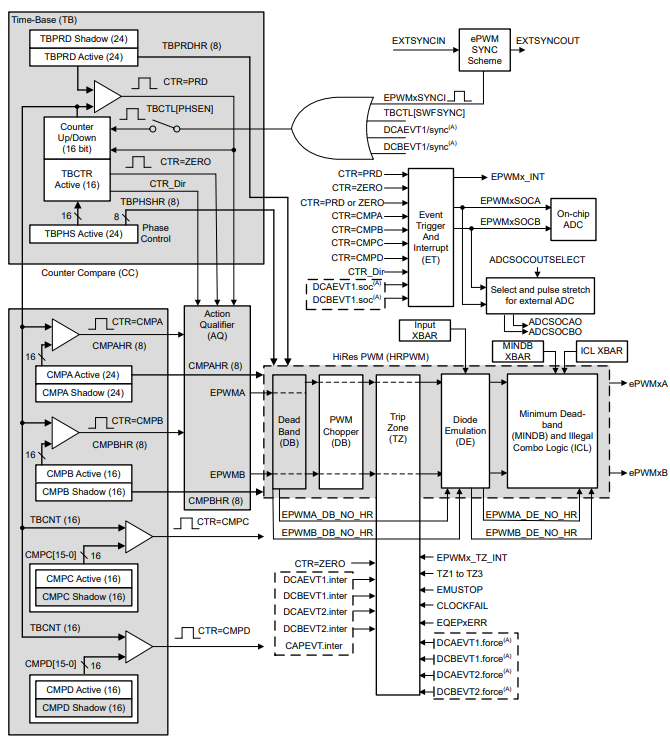
Fig. 5.63 Cdd Pwm module architecture
Note
All duty cycle values may not be valid for a particular configured period. The duty cycle is calculated based on the compare value which is an integer. Period configured in EB tresos or set by calling Cdd_Pwm_SetPeriod() is written directly into the TBPRD register.
In case of asymmetric waveform, the notification at the counter = Zero event is common for both the channels of the PWM instance. The notification count in such scenarios will be only one instead of two.
For example: For asymmetric waveform, if the notification is enabled on both edges for both the channels then the notification count when both the channels have HIGH polarity is (1 for falling of Channel A + 1 for falling of Channel B + 1 for rising edge of both Channels A & B)
This happens because counter=Zero event is common for both the channels and both the outputs have the rising edge at that particular event.
This scenario is not applicable to the Symmetric waveform because both the edges occur at counter=CMP and different events are supported for each output channel.
Cdd_Pwm_EnableNotification & Cdd_Pwm_DisableNotification APIs enable and disable the EPWM interrupt respectively.
5.16.3.1.4. Hardware Features supported in simple mode
Dedicated 16-bit time-base counter with period and frequency control.
Two PWM outputs (EPWMxA and EPWMxB) that can be used in the following configurations -
Two independent PWM outputs with single-edge operation.
Two independent PWM outputs with dual-edge symmetric operation.
One independent PWM output with dual-edge asymmetric operation.
Asynchronous override control of PWM signals through software.
Hardware-locked (synchronized) phase relationship on a cycle-by-cycle basis.
All events can trigger CPU interrupts
Programmable event prescaling minimizes CPU overhead on interrupts.
5.16.3.1.5. Non compliance in simple mode with respect to AUTOSAR spec
Cdd_Pwm_GetOutputState : This API is not supported.
Cdd_Pwm_SetOutputToIdle : API is supported but the change in the output state will not happen immediately. The output will be set to the IDLE state at the end of the period of the wave.
Note
Cdd_Pwm_SetOutputToIdle doesn’t set the PWM output to IDLE state immediately. The API operates in shadow mode so the IDLE state will be effective from CTR=Zero event. All the supported APIs work in shadow mode which means any update in the period, duty cycle, action qualifier actions and IDLE output will happen when the counter is equal to zero.
Simple mode implements AUTOSAR APIs whereas advanced focuses on supporting the hardware features through APIs.
Not all sub-modules are supported in simple mode. Advanced features are accessible through the Advanced Mode APIs.
5.16.3.2. Advanced mode
Advanced mode provides full access to all hardware capabilities, offering granular and precise control over hardware for sophisticated applications.
Description of some of the APIs in advanced mode:
Cdd_Pwm_Init - Only XLINK is enabled for PWM instances
Cdd_Pwm_SetInterruptEventCount - Set interrupt event prescale value (no runtime error will be reported in advanced mode)
Cdd_Pwm_EnableNotification - Enable notification for the PWM instance
Cdd_Pwm_DisableNotification - Disable notification for the PWM instance
Cdd_Pwm_GetVersionInfo - Retrieve software version information of the module
Cdd_Pwm_ConfigureTripZoneNotification should be used to enable/disable trip zone notifications.
5.16.3.2.1. Additional sub-modules thar are supported in Advanced mode
5.16.3.2.1.1. Dead-Band submodule
The dead-band submodule provides a means to delay the switching of a gate signal, thereby allowing time for gates to turn off and preventing a short circuit. This submodule supports independently programmable rising-edge and falling-edge delays with various options for generating the appropriate signal outputs on EPWMxA and EPWMxB.
The key functions of the dead-band module are:
Generating appropriate signal pairs (EPWMxA and EPWMxB) with dead-band relationship from a single EPWMxA input
Programming signal pairs for: -Active high (AH) -Active low (AL) -Active high complementary (AHC) -Active low complementary (ALC)
Adding programmable delay to rising edges (RED)
Adding programmable delay to falling edges (FED)
Can be totally bypassed from the signal path
The dead-band submodule provides a way to delay the switching of the PWM (high to low or low to high). By delaying the transition of PWM signals, you can allow time for the PWM gates to turn off and prevent a short circuit.
The dead-band submodule supports independently programmable rising-edge and falling-edge delays with various options for generating the appropriate signal outputs on EPWMxA and EPWMxB.
Why Dead-band Dead-band control provides a convenient means of combating current shoot-through problems in a power converter. Shoot-through occurs when both the upper and lower gates in the same phase of a power converter are open simultaneously (both gates “on”).This condition shorts the power supply and results in a large current draw. Shoot-through problems occur because transistors open faster than they close, and because high-side and low-side power converter gates are typically switched in a complimentary fashion. Although the duration of the shoot-through current path is finite during PWM cycling, (i.e. the closing gate will eventually shut), even brief periods of a short circuit condition can produce excessive heating and over stress the power converter and power supply.
5.16.3.2.1.2. Chopper submodule
The PWM chopper submodule is used with pulse transformer-based gate drives to control the power switching devices. This submodule uses a high-frequency carrier signal together with the PWM waveform that is generated by the previous submodules (time-base, counter-compare, action-qualifier, and dead-band).
The key functions of the PWM chopper submodule are:
Programmable chopping (carrier) frequency
Programmable pulse width of first pulse
Programmable duty cycle of second and subsequent pulses
Can be fully bypassed if not required
Additionally, this submodule provides an option to include a larger, one-shot (OSHT) pulse width before the sustaining pulses.
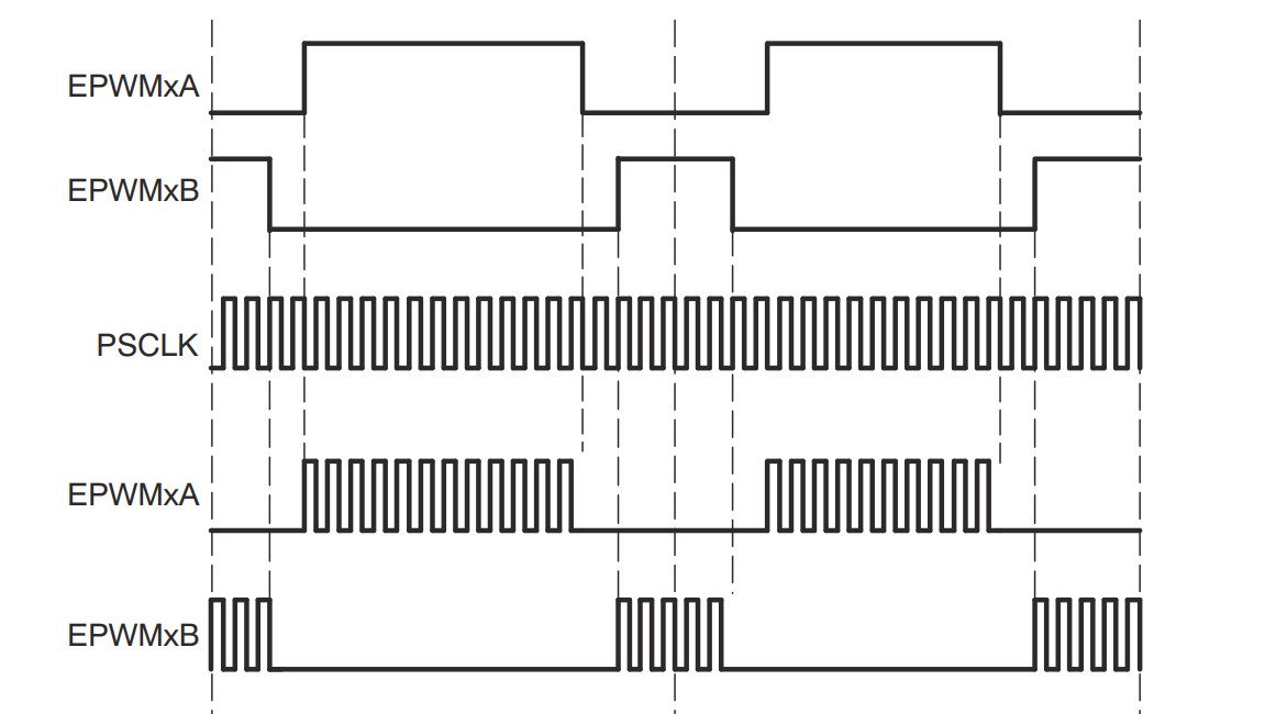
Fig. 5.64 Cdd Pwm Chopper SUB-module Action
5.16.3.2.1.3. Trip-Zone submodule
The trip zone and digital compare submodules provide a protection mechanism to protect the output pins from abnormalities, such as over-voltage, over-current, and excessive temperature rise.
Using the trip-zone is the quickest way to change a PWM output. The trip-zone submodule utilizes a fast, clock-independent logic mechanism to quickly handle fault conditions by forcing the EPWMxA and EPWMxB outputs to a safe, configurable state (such as high, low, or high-impedance). Due to its speed and hardware connection, the trip-zone can be used when interrupts (ISR software) may not be quick enough to protect the hardware in response to over-current conditions or short-circuits.
The trip-zone supports two types of trips
One-shot (OSHT) trips for major short circuits or over current conditions Cycle-by-cycle (CBC) trips for current limiting operation
Trip-zone signals (TZ1-TZ6) can come from several sources. The trip-zone signals are typically as follows:
TZ1-TZ3: Externally from any GPIO pin. A specific GPIO signal can be routed to the EPWM Trip Zone using the INPUT X-BAR Module TZ4: Internally from an inverted eQEP error signal (TZ4) TZ5: Internally from system clock failure (TZ5) TZ6: Internally from an emulation stop output from the CPU (TZ6).
Additionally, numerous trip-zone source signals can be generated from the digital-compare subsystem.
The power drive protection is a safety feature that is provided for the safe operation of systems such as power converters and motor drives. It can be used to inform the monitoring program of motor drive abnormalities such as over-voltage, over-current, and excessive temperature rise. If the power drive protection interrupt is unmasked, the PWM output pins will be put in a safe state immediately after the pin is driven low. An interrupt will also be generated.
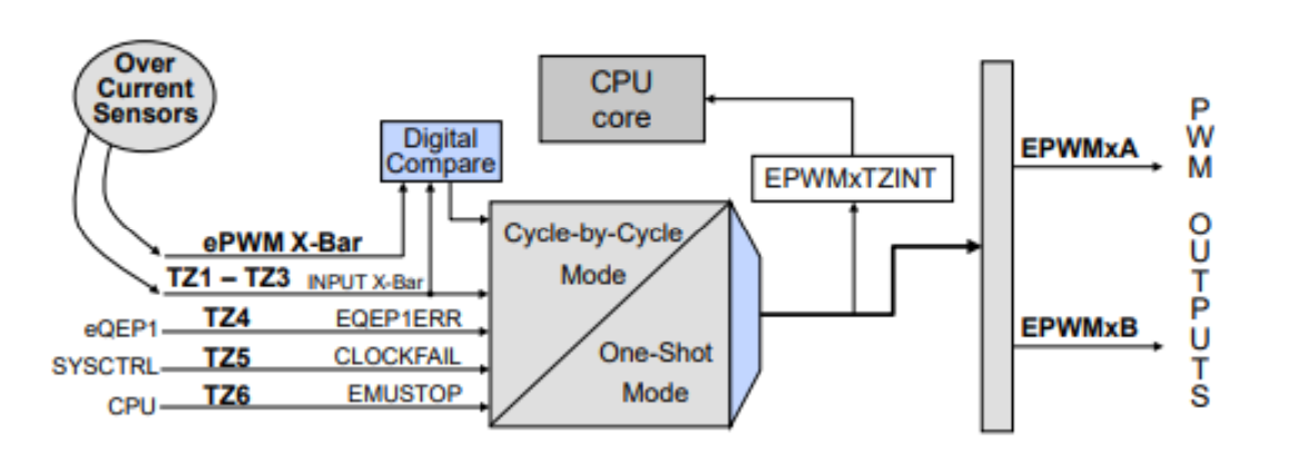
Fig. 5.65 Cdd Pwm Trip Zone Block
5.16.3.2.1.4. EPWM X-BAR
The EPWM X-BAR is used to route various internal and external signals to the EPWM modules. Eight trip signals from the EPWM X-BAR are routed to all of the EPWM modules. The EPWM XBAR can select a single signal or logically OR up to 32 signals.
5.16.3.2.1.5. Digital Compare (DC) submodule
The digital-compare submodule, like the trip-zone, can also help protect the output pins from abnormalities, such as over-voltage, over-current, and excessive temperature rise. This submodule compares signals external to the EPWM module, such as a signal from the CMPSS analog comparators, to directly generate PWM digital-compare events or actions. These digital-compare events or actions can then used by the trip-zone, time-base, and event-trigger submodules to trip the EPWM which can: Generate a trip interrupt Sync the EPWM Generate an ADC start of conversion
You can also use the digital-compare submodule ‘Blanking’ functionality to temporarily disable PWM actions for a period of time to eliminate noise effects and it is configurable.
A digital-compare event is generated when one or more of its selected inputs are either high or low. The inputs to the digital-compare submodule are sourced from INPUT X-BAR, EPWM X-BAR and trip-zone input pins.
To use the digital-compare events, the user selects the input for each signal (DCAH, DCAL, DCBH, DCBL) and the state of each signal that will trigger each compare.
5.16.3.2.1.6. Event Trigger submodule
The event-trigger submodule can use the events generated by the time-base, counter-compare, and digital-compare submodules to trigger two types of actions: Generate an interrupt to the CPU Generate a start-of-conversion (SOC) pulse to the ADC
The event-trigger submodule also incorporates pre-scaling logic to issue an interrupt request or ADC SOC on every event or up to every fifteenth event. These event triggers can occur at a number of configurable time such as when the time-base counter equals zero, period, zero or period, or on the up-count or down-count match of a counter-compare value (CMPx). The digital-compare subsystem can also be used to generate an ADC SOC based on one or more compare events. Notice counter-up and counter-down triggers are independent and separate.
5.16.3.2.1.7. XCMP mode
Instead of generating a single pulse within a single PWM period, generation of up to a max of 4 pulses within a single PWM period is possible with XCMP mode. CMPA and CMPB will have two options to allocate extended compare registers (XCMP1-8) one of two ways. Allocate all XCMP1-8 to CMPA or allocate XCMP1-4 to CMPA and XCMP5-8 to CMPB.
When XCMP mode is enabled, the counter direction can only be in up-count mode. The above event waveform diagram shows extended counter compare matches which are fed into action qualifer. At the end of every period, the shadow register set is loaded to the active registers to generate a new waveform.
Loading from shadow to active can be configured in two ways: Load Once Load once has three shadow register sets to load once from. The additional configurability is to select which shadow register set to load from first.Load multiple allows configurability to cycle through the shadow registers depending on how many shadow register sets are required.
Load Multiple There are 4 configurations with load multiple in using the shadow register sets. The four possible load multiple schemes can be using only active register, shadow register 1, shadow register 1 and 2, or from all three shadow registers. If choosing all three shadow register, load multiple will start with shadow register 3 then load shadow register 2 then shadow register 1 on the next time-base counter equals to zero events. Once load multiple has cycled through all shadow register sets, load multiple will not cycle through the shadow register sets again until the load start bit is enabled again.
Note: There only are allowable repetition for shadow buffer set 2 and 3
Below is an example of XCMP mode
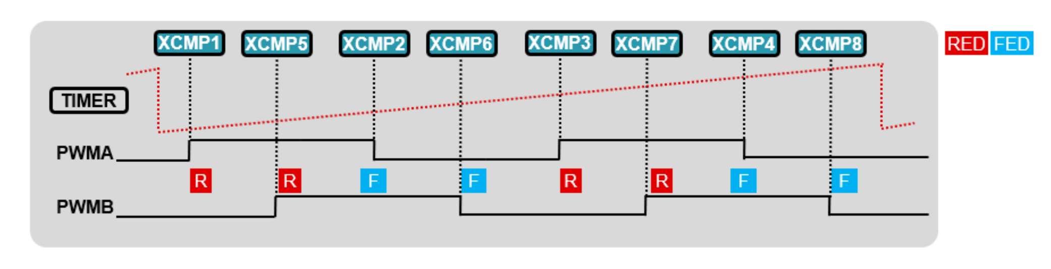
Fig. 5.66 Cdd Pwm XCMP example
5.16.3.2.1.8. Diode Emulation submodule
Diode emulation is used in conjunction with CMPSS module to drive the EPWM outputs to a certain state when the CMPSS sends out trip signal. The outputs from the trip zone will be sent to the Diode Emulation block.
Features of the diode emulation include: Ability to send out a trip signal (DEMONTRIP) if the diode emulation mode is active for more than an allowable amount time. Ability to force the PWM outputs to be same as trip signals, low or high.
Inputs to the diode emulation block come from the CMPSS and input x-bar. The trip zone submodule’s outputs are also routed through this block. Diode emulation can be disabled to carry through the trip zone module’s output. The below waveform is to demonstrate a common use case for this feature which is current detection. The red signal can represent current in a system. The CMPSS will configure the original DACVAL for high and low thresholds. Diode emulation support within CMPSS, will allow configurability for setting another pair of DACVAL thresholds if the ePWM module enters diode emulation.
Since the diode emulation module takes input signal from CMPSSnTRIPH and CMPSSnTRIPL, only when the current goes past the original CMPSS threshold the diode emulation sets the DACVAL_H2 and DACVAL_L2. During this new threshold region, the PWM outputs will change accordingly to the PWM’s diode emulation set outputs and diode emulation mode will be active until the current resumes normal operation. Once current is within normal operating regions, the CMPSS resumes its original DACVAL thresholds and PWM outputs will resume.
First the DEACTIVE flag is set to high because a TRIPH or TRIPL event has occurred. Once in diode emulation mode, EPWMxA_DE is configured to follow TRIPL, and EPWMxB_DE is configured to follow TRIPH. The outputs will continue to follow TRIPH/L until diode emulation mode has been exited. Diode emulation mode can be exited either cycle-by-cycle clear or by software. Cycle-by-cycle clear will evaluate on every PWMSYNCOUT event if the trip condition is not present.
5.16.3.2.1.9. Minimum Dead Band (MINDB) & Illegal Combo Logic (ICL) submodule
The EPWM Minimum Dead-Band submodule is similar to the dead-band submodule in applying a configurable amount of delay between PWM modules. The goal of this feature is to ensure gates are not on at the same time and prevent a short circuit. In the figure below, when a falling edge occurs on EPWMxA the minimum delay set will apply to EPWMxB’s output. When a falling edge occurs on EPWMxB, a minimum delay is applied to EPWMxA.
The Illegal Combo Logic (ICL) submodule monitors PWM outputs to detect and prevent illegal combinations of signals that could potentially damage power electronics hardware. It provides hardware-level protection against scenarios where multiple switches in a power converter might be turned on simultaneously due to software errors or other fault conditions. When an illegal combination is detected, the ICL can force the outputs to a safe state, helping to prevent catastrophic failures in the power stage.
5.16.3.2.2. EPWM MINDB and ICL X-BARs
The purpose of Minimum Dead-band (MINDB) and Illegal Combination Logic (ICL) XBARs is to expand functionality of the Minimum Dead-band and Illegal Combination Logic submodule of the EPWM by routing in signals from the diode emulation logic module, minimum dead-band module, and CLB. Their functionality is similar to the Input XBAR module, meaning only a single input to the XBARs can be routed to the output, unlike the Output XBAR for example, where multiple inputs can be combined as a logical OR and sent to the output.
5.16.3.2.2.1. High-resolution PWM(HRPWM) submodule
The EPWM module is capable of significantly increasing its time resolution capabilities over the standard conventionally derived digital PWM. This is accomplished by adding 8-bit extensions to the counter-compare register (CMPxHR), time-base period register (TBPRDHR), and time-base phase register (TBPHSHR) to provide a finer time granularity for edge positioning control. This is known as high-resolution PWM (HRPWM) and it is based on micro edge positioner (MEP) technology.
MEP logic is capable of positioning an edge very finely by sub-dividing one coarse system clock of the conventional PWM generator with time step accuracy on the order of 150 picoseconds (see your device documentation for specifications). A self-checking software diagnostic (SFO Library) is used to determine if the MEP logic is running optimally, and it can calibrate the MEP logic under all operating conditions to account for variations caused by temperature, voltage, and process. HRPWM is typically used when the PWM resolution falls below approximately 9 or 10 bits.
HRPWM significantly increases the resolution of conventionally derived digital PWM. Adds 8-bit extensions to counter-compare registers (CMPxHR), time-base period register (TBPRDHR) and time-base phase register (TBPHSHR) for micro edge positioning (MEP) control
The micro edge positioner (MEP) logic is capable of placing an edge in one of 255 discrete time steps. The MEP step size varies based on worst-case process parameters, operating temperature, and voltage. MEP step size increases with decreasing voltage and increasing temperature and decreases with increasing voltage and decreasing temperature. Applications that use the HRPWM feature can use the TI-supplied MEP scale factor optimization (Cdd_Pwm_Sfo) software function. The Cdd_Pwm_Sfo function helps to dynamically determine the number of MEP steps per EPWMCLK period while the HRPWM is in operation.
To utilize the MEP capabilities effectively, the correct value for the MEP scaling factor needs to be known by the software. To accomplish this, the HRPWM module has built in self-check and diagnostic capabilities that can be used to determine the optimum MEP scale factor value for any operating condition.
There are 3 HRPWM calibration units in the device. The calibration unit ID should be passed as a parameter to the Cdd_Pwm_Sfo API to select the respective calibration unit.
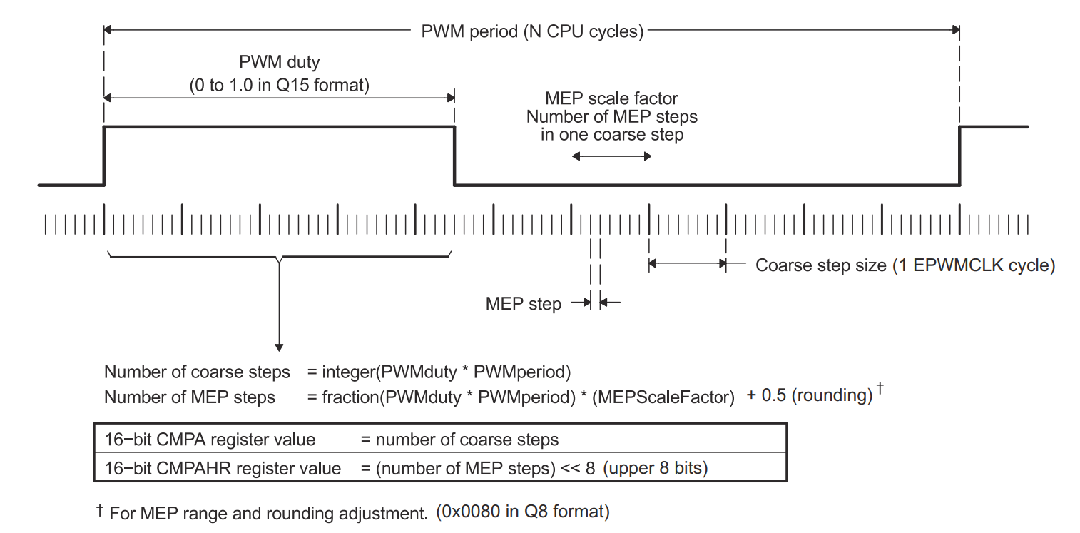
Fig. 5.67 Cdd Pwm Hrpwm operting logic
Note
CDD_PWM_HRPWM_MEP_CTRL_RISING_AND_FALLING_EDGE(both rising & falling edges) MEP Edge select type is not supported for CMPAHR & CMPBHR. MEP control of both edges configuration is for TBPHSHR or TBPRDHR. Only MEP control of rising edge and MEP control of falling edge controls CMPAHR/CMPBHR.
5.16.3.2.3. XLINK
XLINK feature, which allows synchronization between multiple EPWM instances, can only be enabled for each EPWM instance in the EB tresos configuration tool by adding the instance under the CddPwmXlinkConfig/CddPwmLinkHwUnit container. It’s important to note that despite the hardware supporting a XLINK region for each instance, the driver reserves a single XLINK region which is the respective XLINK region of the first EPWM instance that is added to the container CddPwmXlinkConfig/CddPwmLinkHwUnit .
Runtime configuration of XLINK is not supported. This configuration must be done during the initial setup phase, and cannot be modified during runtime. XLINK enabling for the EPWM instances is done in Cdd_Pwm_Init() API.
5.16.3.2.4. Hardware Features supported in advanced mode
Features Supported at a high level are: (All hardware features) The following features in addition to simple mode feature:
Programmable phase-control support for lag or lead operation relative to other EPWM modules.
Hardware-locked (synchronized) phase relationship on a cycle-by-cycle basis.
Dead-band generation with independent rising and falling edge delay control.
Programmable trip zone allocation of both cycle-by-cycle trip and one-shot trip on fault conditions.
A trip condition can force either high, low, or high-impedance state logic levels at PWM outputs.
All events can trigger both CPU interrupts and ADC start of conversion (SOC)
PWM chopping by high-frequency carrier signal, useful for pulse transformer gate drives.
Note
Cdd_Pwm_DeInit API is not supported in advanced mode. Application needs to take care of setting the PWM outputs to the IDLE state.
5.16.4. Source files
📦f29h85x_mcal
┣ 📂build
┣ 📂docs
┣ 📂drivers
┃ ┣ 📂BSW_Stubs
┃ ┣ 📂Can
┃ ┣ 📂Cdd_Adc
┃ ┣ 📂Cdd_Ecap
┃ ┣ 📂Cdd_Ipc
┃ ┣ 📂Cdd_Pwm
┃ ┃ ┣ 📂include
┃ ┃ ┃ ┣ 📜Cdd_Pwm.h : Contains the API declarations of the Cdd_Pwm driver to be used by upper layers.
┃ ┃ ┃ ┣ 📜Cdd_Pwm_Priv.h : Declaration of the private APIs.
┃ ┃ ┣ 📂src
┃ ┃ ┃ ┣ 📜Cdd_Pwm.c : Implementation of the Cdd_Pwm public APIs.
┃ ┃ ┃ ┣ 📜Cdd_Pwm_Irq.c : Implementation for Cdd_Pwm interrupts handlers.
┃ ┃ ┃ ┗ 📜Cdd_Pwm_Priv.c : Implementation of the private APIs
┃ ┃ ┗ 📜CMakeLists.txt
┃ ┣ 📂Cdd_Sent
┃ ┣ 📂Cdd_Uart
┃ ┣ 📂Cdd_Xbar
┃ ┣ 📂Dio
┃ ┣ 📂Gpt
┃ ┣ 📂hw_include
┃ ┣ 📂Lin
┃ ┣ 📂Mcal_Lib
┃ ┣ 📂Mcu
┃ ┣ 📂Port
┃ ┣ 📂Spi
┃ ┗ 📂Wdg
┣ 📂examples
┣ 📂plugins
┣ 📜CMakeLists.txt
┗ 📜CMakePresets.json
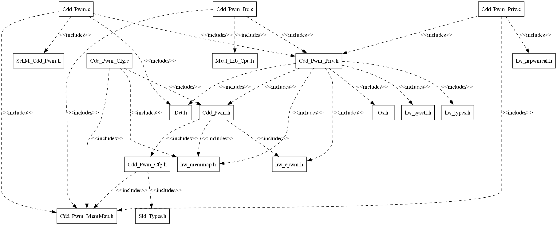
Fig. 5.68 Cdd Pwm Header File Structure
5.16.5. Module requirements
5.16.5.1. Memory Mapping
The driver follows the AUTOSAR memory mapping strategy. All memory sections should be stored in memory as per AUTOSAR specifications, considering initialization policy, alignment requirements, safety classification, and core scope where applicable.
Reference memory map files can be found at:
{MCAL_INSTALL_PATH}\drivers\BSW_Stubs\MemMap\include
The memory sections are organized according to AUTOSAR specifications to ensure proper placement of code and data in different memory regions based on their usage and access patterns.
5.16.5.2. Scheduling
None
5.16.5.3. Error handling
5.16.5.3.1. Development Error Reporting
Development errors are reported to the DET using the service Det_ReportError(), when enabled. The driver interface contains the MACRO declaration of the error codes to be returned.
5.16.5.4. Error codes in simple mode
Type of Error |
Related Error code |
Value (Hex) |
|---|---|---|
API called when the driver is not initialized |
CDD_PWM_E_UNINIT |
0x0AU |
Init API called when the driver is already initialized |
CDD_PWM_E_ALREADY_INITIALIZED |
0x0BU |
Init API called with invalid pointer |
CDD_PWM_E_PARAM_POINTER |
0x0CU |
API called with invalid ID(parameter) |
CDD_PWM_E_INVALID_ID |
0x0DU |
API called for the PWM instance whose has no notification pointer available |
CDD_PWM_E_NOTIF_CAPABILITY |
0x0EU |
API called for the PWM instance whose channel class is not variable period |
CDD_PWM_E_CHANNEL_CLASS |
0x0FU |
API called when the channel configured for the notification is invalid |
CDD_PWM_E_INVALID_EDGENOTIFICATION |
0x11U |
API called when the edge notification type is not valid |
CDD_PWM_E_INVALID_NOTIFICATION |
0x12U |
API called when the event count is invalid/out-of-range |
CDD_PWM_E_INVALID_EVENT_COUNT |
0x13U |
API called with invalid/out-of-range duty cycle value |
CDD_PWM_E_INVALID_DUTY_CYCLE |
0x18U |
5.16.5.4.1. Runtime Errors in simple mode
Type of Error |
Related Error code |
Value (Hex) |
|---|---|---|
API called whose notification is already enabled or invalid channel notification is called for the instance |
CDD_PWM_E_NOTIF_ALREADY_ENABLED |
0x10U |
Cdd_Pwm_SetInterruptEventCount API called for an instance whose notification is enabled |
CDD_PWM_E_BUSY |
0x15U |
Cdd_Pwm_EnableNotification API called when the InterruptEventCount is zero |
CDD_PWM_E_INVALID_INTEVTCOUNT |
0x16U |
5.16.5.5. Error codes in advanced mode
Type of Error |
Related Error code |
Value (Hex) |
|---|---|---|
API called when the driver is not initialized |
CDD_PWM_E_UNINIT |
0x0AU |
Init API called when the driver is already initialized |
CDD_PWM_E_ALREADY_INITIALIZED |
0x0BU |
Init API called with invalid pointer |
CDD_PWM_E_PARAM_POINTER |
0x0CU |
API called with invalid ID(parameter) |
CDD_PWM_E_INVALID_ID |
0x0DU |
API called for the PWM instance whose has no notification pointer available |
CDD_PWM_E_NOTIF_CAPABILITY |
0x0EU |
API called with invalid output channel |
CDD_PWM_E_INVALID_OUTPUT_CHANNEL |
0x0FU |
API called when the event count is invalid/out-of-range |
CDD_PWM_E_INVALID_VALUE |
0x13U |
API called with invalid prescale value |
CDD_PWM_E_INVALID_PRESCALE |
0x14U |
API called with invalid counter compare value |
CDD_PWM_E_INVALID_CTRCOMPARE |
0x15U |
API called with invalid event |
CDD_PWM_E_INVALID_EVENT |
0x16U |
API called with invalid polarity |
CDD_PWM_E_INVALID_POLARITY |
0x17U |
API called with invalid ADCSOC type |
CDD_PWM_E_INVALID_ADCSOC_TYPE |
0x18U |
API called with invalid event source |
CDD_PWM_E_INVALID_EVENT_SRC |
0x19U |
API called with invalid shadow set |
CDD_PWM_E_INVALID_SHDSET |
0x1AU |
5.16.6. Safety Mechanism
TI Diagnostic Unique Identifier |
Summary |
Description |
|---|---|---|
PWM6 |
Lock Mechanism for Control Registers |
Critical ePWM control registers are protected using a lock mechanism. Once the LOCK register bits are set, write access is blocked until a reset occurs |
PWM16 |
Fault Avoidance using Minimum Dead Band Logic |
Minimum Dead Band logic can be configured to guarantee a minimum inactive gap between the active pulse phases of PWM channels, preventing crossover faults caused by faults in the preceding digital logic |
PWM17 |
Fault Avoidance using Illegal Combo Logic |
Illegal Combination Logic can be configured to guarantee safe PWM output values for illegal input signal combinations, making the PWM system immune to faults that could result in undesirable outputs |
PWM18 |
Diode Emulation Mode Monitoring |
Diode Emulation mode monitoring can be configured to generate a TRIP event if the ePWM module remains in Diode Emulation mode longer than the configured threshold, protecting against faults in the Diode Emulation logic |
Note
The above safety mechanism (features) are available only when the PWM driver is configured in Advanced mode.
Note
More details of Safety Mechanisms can be found in Safety Manual.
5.16.7. Silicon errata workarounds and recommendation
For detailed silicon errata, please check the latest Errata at https://www.ti.com/product/F29H859TU-Q1.
Advisory |
Revisions Affected |
Workaround in MCAL driver |
Recommended actions for user |
|---|---|---|---|
ePWM: An ePWM Glitch can Occur if a Trip Remains Active at the End of the Blanking Window |
0, A, B, C |
No workaround is implemented in the CDD PWM driver. |
Extend or reduce the blanking window to avoid any undesired trip action. |
ePWM: ePWM TZFRC and TZCLR Events may be Missed When PERCLKDIVSEL.EPWMCLKDIV = 1 |
0, A, B, C |
No workaround is implemented in the CDD PWM driver. |
1. Configure EPWMCLK = PLLSYSCLK ( |
ePWM: ESM Source for Trip Zone is not Supported |
0, A, B, C |
No workaround is implemented in the CDD PWM driver. |
Use the error source to generate an NMI interrupt from the respective ESM CPU instance. Within the NMI interrupt, issue a software write using |
ePWM: ePWM One-Shot/CBC Trip Event DCxEVTy.force Does Not Set the Trip Condition |
0, A, B, C |
No workaround is implemented in the CDD PWM driver. |
For devices with |
ePWM: For ePWMs Using Global Load in One-Shot Load Mode, Global Load of Registers may get Delayed When a Write to the GLDCTL2.OSHTLD Register Occurs Within 3 TBCLKs of the Global Load Event |
0, A, B, C |
No workaround is implemented in the CDD PWM driver. |
Any writes to the |
HRPWM: HRPWM High-Resolution Period Shadow to Active Loading Occurs Every ZERO Event, Even if Shadow to Active Load for Period is Set to Only Load on SYNC |
0, A, B, C |
No workaround is implemented in the CDD PWM driver. |
When using high-resolution period, the sync event is ignored, and shadow-to-active loading occurs every ZERO event. If high-resolution period is disabled, the sync event is not ignored, and shadow-to-active loading occurs on a sync event. |
5.16.8. Used resources
5.16.8.1. Interrupt Handling
Cdd_Pwm driver provides ISRs. The ISRs are implemented in the Cdd_Pwm_Irq.c file. Interrupt and the category should be selected in the Cdd_Pwm plugin.The Interrupt ID associated with the PWM instance is mentioned in the TRM (also, please refer the Example application).
Cdd_Pwm Instance |
Interrupt Name |
Interrupt handler |
|---|---|---|
EPWM1 |
EPWM1_INT |
Cdd_Pwm_Epwm1_IntIsr |
EPWM2 |
EPWM2_INT |
Cdd_Pwm_Epwm2_IntIsr |
EPWM3 |
EPWM3_INT |
Cdd_Pwm_Epwm3_IntIsr |
EPWM4 |
EPWM4_INT |
Cdd_Pwm_Epwm4_IntIsr |
EPWM5 |
EPWM5_INT |
Cdd_Pwm_Epwm5_IntIsr |
EPWM6 |
EPWM6_INT |
Cdd_Pwm_Epwm6_IntIsr |
EPWM7 |
EPWM7_INT |
Cdd_Pwm_Epwm7_IntIsr |
EPWM8 |
EPWM8_INT |
Cdd_Pwm_Epwm8_IntIsr |
EPWM9 |
EPWM9_INT |
Cdd_Pwm_Epwm9_IntIsr |
EPWM10 |
EPWM10_INT |
Cdd_Pwm_Epwm10_IntIsr |
EPWM11 |
EPWM11_INT |
Cdd_Pwm_Epwm11_IntIsr |
EPWM12 |
EPWM12_INT |
Cdd_Pwm_Epwm12_IntIsr |
EPWM13 |
EPWM13_INT |
Cdd_Pwm_Epwm13_IntIsr |
EPWM14 |
EPWM14_INT |
Cdd_Pwm_Epwm14_IntIsr |
EPWM15 |
EPWM15_INT |
Cdd_Pwm_Epwm15_IntIsr |
EPWM16 |
EPWM16_INT |
Cdd_Pwm_Epwm16_IntIsr |
EPWM17 |
EPWM17_INT |
Cdd_Pwm_Epwm17_IntIsr |
EPWM18 |
EPWM18_INT |
Cdd_Pwm_Epwm18_IntIsr |
The trip zone interrupts are only supported in advanced mode.
Cdd_Pwm Instance |
Interrupt Name |
Interrupt handler |
|---|---|---|
EPWM1 |
EPWM1_TZINT |
Cdd_Pwm_Epwm1_TzIntIsr |
EPWM2 |
EPWM2_TZINT |
Cdd_Pwm_Epwm2_TzIntIsr |
EPWM3 |
EPWM3_TZINT |
Cdd_Pwm_Epwm3_TzIntIsr |
EPWM4 |
EPWM4_TZINT |
Cdd_Pwm_Epwm4_TzIntIsr |
EPWM5 |
EPWM5_TZINT |
Cdd_Pwm_Epwm5_TzIntIsr |
EPWM6 |
EPWM6_TZINT |
Cdd_Pwm_Epwm6_TzIntIsr |
EPWM7 |
EPWM7_TZINT |
Cdd_Pwm_Epwm7_TzIntIsr |
EPWM8 |
EPWM8_TZINT |
Cdd_Pwm_Epwm8_TzIntIsr |
EPWM9 |
EPWM9_TZINT |
Cdd_Pwm_Epwm9_TzIntIsr |
EPWM10 |
EPWM10_TZINT |
Cdd_Pwm_Epwm10_TzIntIsr |
EPWM11 |
EPWM11_TZINT |
Cdd_Pwm_Epwm11_TzIntIsr |
EPWM12 |
EPWM12_TZINT |
Cdd_Pwm_Epwm12_TzIntIsr |
EPWM13 |
EPWM13_TZINT |
Cdd_Pwm_Epwm13_TzIntIsr |
EPWM14 |
EPWM14_TZINT |
Cdd_Pwm_Epwm14_TzIntIsr |
EPWM15 |
EPWM15_TZINT |
Cdd_Pwm_Epwm15_TzIntIsr |
EPWM16 |
EPWM16_TZINT |
Cdd_Pwm_Epwm16_TzIntIsr |
EPWM17 |
EPWM17_TZINT |
Cdd_Pwm_Epwm17_TzIntIsr |
EPWM18 |
EPWM18_TZINT |
Cdd_Pwm_Epwm18_TzIntIsr |
Note
Same Interrupt Category needs to be configured in both Cdd_Pwm and OS Module. Both the channels under a EPWM/PWM instance share the same interrupt.
5.16.8.2. Instance support
CPU instances |
supported |
|---|---|
CPU 1 |
YES |
CPU 2 |
NO |
CPU 3 |
NO |
5.16.8.3. Hardware-Software Mapping
Below image shows Cdd_Pwm driver Hardware-Software mapping. For more information related to HW/SW mapping, refer the F29x Reference Manual.
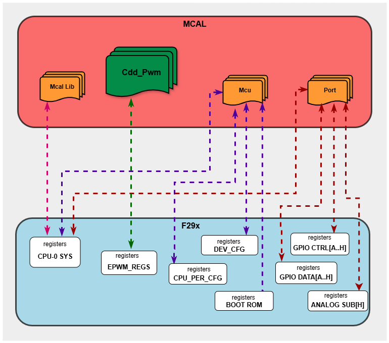
Fig. 5.69 Cdd_Pwm HW/SW Mapping
5.16.9. Integration description
5.16.9.1. Dependent modules
5.16.9.1.1. DET
This driver depends on the DET in order to report development and runtime errors. The detection of development errors is configurable ON/OFF. The switch CDD_PWM_DEV_ERROR_DETECT will activate or deactivate the detection of development errors. Runtime errors are reported even when CDD_PWM_DEV_ERROR_DETECT is OFF.
5.16.9.1.2. MCU
MCU Module is required for the PWM clock initialization.
5.16.9.1.3. OS
The Cdd_Pwm driver uses interrupts and therefore there is a dependency on the OS, which configures the interrupt sources.
5.16.9.1.4. PORT
The Port module configures the port pins used for the PWM driver in the EPWM mode. Hence, the Port driver has to be initialized prior to use PWM functions and to generate proper PWM output. Otherwise unpredictable output might be generated.
5.16.9.1.5. SchM
If multiple AUTOSAR runnables have access to the same Data Store Memory block, the exported AUTOSAR specification enforces data consistency by using an AUTOSAR exclusive area. With this specification, the runnables have mutually exclusive access to the per-instance memory global data, which prevents data corruption. Beside the OS, the BSW Scheduler provides functions that CDD PWM module calls at begin and end of critical sections. This implementation requires 1 level of exclusive access to guard critical sections.
The data consistency mechanism that has to be applied to an ExclusiveArea might be domain, ECU or even project specific. The decision which mechanism has to be applied by RTE / Basic Software Scheduler is taken during ECU integration by setting the Exclusive Area configuration parameter RteExclusiveAreaImplMechanism. This parameter is an input for RTE generator.
For CDD_PWM Module, data consistency and exclusive access to critical sections are required for the following sections as shown in the table below:
Exclusive Area Functions used |
CDD_PWM Function calling Exclusive Area |
Need for Exclusive Area |
Recommended Exclusive Area Mapping |
|---|---|---|---|
CDD_PWM_EXCLUSIVE_AREA_0 |
Cdd_Pwm_SetDutyCycle |
To protect against multiple access for shared resources |
ALL_INTERRUPT_BLOCKING : All interrupts should be blocked as this API’s can be called in the interrupts. |
5.16.9.2. Resource Allocator
The PWM module uses the Resource Allocator to allocate PWM peripheral instances to CPU cores and configure their memory-mapped base addresses. Each allocation is placed inside a Context that maps to a CPU core (e.g. CPU1). The CurrentContext parameter in the Resource Allocator selects which Context is active for MCAL execution. See the Resource Allocator Module User Guide for details on configuring device-specific settings.
The PWM Context container supports two types of allocations:
Cdd_PwmAllocatedInstance: Allocates an EPWM hardware instance (e.g.EPWM1). Each instance has both a BaseAddr and an XlinkBaseAddr, both auto-calculated based on the selected instance and frame.CddPwmHrpwmCalInstance: Allocates an HRPWM calibration instance (e.g.HRPWMCAL1). BaseAddr is auto-calculated based on the selected instance and frame.
Each allocation supports Frame (FRAME0–FRAME3), DebugHaltEnabled, and StandbyModeEnabled parameters.
5.16.9.2.1. Resource Allocator Usage Example
To allocate EPWM1 to CPU1 using FRAME0:
In the Resource Allocator configuration, create a new
Cdd_PwmAllocatedInstanceunder the CPU1 ContextSet InstanceName to
EPWM1Set Frame to
FRAME0The BaseAddr will be automatically calculated as
EPWM1_BASE_FRAME(0U)The XlinkBaseAddr will be automatically calculated as
EPWM1XLINK_BASE_FRAME(0U)Optionally configure DebugHaltEnabled and StandbyModeEnabled
Resource Allocator Configuration:
├── Context (Core: CPU1)
│   └── Cdd_Pwm
│       ├── Cdd_PwmAllocatedInstance
│       │   ├── InstanceName: EPWM1
│       │   ├── Frame: FRAME0
│       │   ├── BaseAddr: EPWM1_BASE_FRAME(0U)  [auto-calculated]
│       │   ├── XlinkBaseAddr: EPWM1XLINK_BASE_FRAME(0U)  [auto-calculated]
│       │   ├── DebugHaltEnabled: true
│       │   └── StandbyModeEnabled: true
│       └── CddPwmHrpwmCalInstance
│           ├── InstanceName: HRPWMCAL1
│           ├── Frame: FRAME0
│           └── BaseAddr: HRPWMCAL1_BASE_FRAME(0U)  [auto-calculated]
5.16.10. Configuration
The Cdd_Pwm Driver implementation supports one configuration variant Pre-Compile config. The driver expects generated Cdd_Pwm_Cfg.h to be present as input file. The associated Cdd_Pwm driver configuration generated source files are Cdd_Pwm_Cfg.c
The generated configuration files should not be modified manually. The config tool Elektrobit Tresos should be used to modify the configuration files.
5.16.10.1. Configuration Parameters
5.16.10.1.1. CddPwmConfigSet
This container contains the configuration parameters and sub containers of the AUTOSAR Pwm instance.
5.16.10.1.1.1. CddPwmAdvancedMode
Item |
|
|---|---|
Name |
CddPwmAdvancedMode |
Description |
Enables/disables the advanced mode for the PWM driver. |
Origin |
Texas Instruments |
Post-Build-Variant-Value |
false |
Value-Configuration-Class |
– |
Pre-Compile-Time |
VARIANT-PRE-COMPILE |
Default-value |
false |
5.16.10.1.1.2. CddPwmHwUnitConfig
Configuration of an individual PWM instance.
5.16.10.1.1.3. CddPwmInstance
Item |
|
|---|---|
Name |
CddPwmInstance |
Description |
Pwm hardware instance. |
Origin |
Texas Instruments |
Post-Build-Variant-Value |
false |
Value-Configuration-Class |
– |
Pre-Compile-Time |
VARIANT-PRE-COMPILE |
Default-value |
1 |
5.16.10.1.1.4. CddPwmHwId
Item |
|
|---|---|
Name |
CddPwmHwId |
Description |
Symbolic ID of the PWM instance. |
Origin |
Texas Instruments |
Post-Build-Variant-Value |
false |
Value-Configuration-Class |
– |
Pre-Compile-Time |
VARIANT-PRE-COMPILE |
Default-value |
0 |
5.16.10.1.1.5. CddPwmEmulationMode
Item |
|
|---|---|
Name |
CddPwmEmulationMode |
Description |
Emulation mode for the EPWM instance. |
Multiplicity-Configuration-Class |
– |
Pre-Compile Time |
VARIANT-PRE-COMPILE |
Origin |
Texas Instruments |
Post-build-variant-multiplicity |
false |
Post-Build-Variant-Value |
false |
Value-Configuration-Class |
– |
Pre-Compile-Time |
VARIANT-PRE-COMPILE |
Default-value |
CDD_PWM_EMULATION_STOP_AFTER_NEXT_TB |
Range |
CDD_PWM_EMULATION_STOP_AFTER_NEXT_TB |
5.16.10.1.1.6. CddPwmClockDivider
Item |
|
|---|---|
Name |
CddPwmClockDivider |
Description |
Time base clock pre-scale value. |
Origin |
Texas Instruments |
Post-Build-Variant-Value |
false |
Value-Configuration-Class |
– |
Pre-Compile-Time |
VARIANT-PRE-COMPILE |
Default-value |
CDD_PWM_CLOCK_DIVIDER_1 |
Range |
CDD_PWM_CLOCK_DIVIDER_1 |
5.16.10.1.1.7. CddPwmHighSpeedClockDivider
Item |
|
|---|---|
Name |
CddPwmHighSpeedClockDivider |
Description |
High speed clock divider for the PWM instance. |
Origin |
Texas Instruments |
Post-Build-Variant-Value |
false |
Value-Configuration-Class |
– |
Pre-Compile-Time |
VARIANT-PRE-COMPILE |
Default-value |
CDD_PWM_HSCLOCK_DIVIDER_1 |
Range |
CDD_PWM_HSCLOCK_DIVIDER_1 |
5.16.10.1.1.8. CddPwmFrequency
Item |
|
|---|---|
Name |
CddPwmFrequency |
Description |
This parameter defines the frequency of the PWM instance. |
Origin |
Texas Instruments |
Post-Build-Variant-Value |
false |
Value-Configuration-Class |
– |
Pre-Compile-Time |
VARIANT-PRE-COMPILE |
Default-value |
1.0E8 |
Max-value |
2.0E8 |
Min-value |
55803.0 |
5.16.10.1.1.9. CddPwmInterruptEnable
Item |
|
|---|---|
Name |
CddPwmInterruptEnable |
Description |
Enables/disables the interrupt for the PWM instance. |
Origin |
Texas Instruments |
Post-Build-Variant-Value |
false |
Value-Configuration-Class |
– |
Pre-Compile-Time |
VARIANT-PRE-COMPILE |
Default-value |
true |
5.16.10.1.1.10. CddPwmInterruptCategory
Item |
|
|---|---|
Name |
CddPwmInterruptCategory |
Description |
This parameters defines the category of the interrupt. |
Origin |
Texas Instruments |
Post-Build-Variant-Value |
false |
Value-Configuration-Class |
– |
Pre-Compile-Time |
VARIANT-PRE-COMPILE |
Default-value |
ISR_CAT1_RTINT |
Range |
ISR_CAT1_INT |
5.16.10.1.1.11. CddPwmInterruptNotification
Item |
|
|---|---|
Name |
CddPwmInterruptNotification |
Description |
Definition of the callback function. |
Multiplicity-Configuration-Class |
– |
Pre-Compile Time |
VARIANT-PRE-COMPILE |
Origin |
Texas Instruments |
Post-build-variant-multiplicity |
false |
Post-Build-Variant-Value |
false |
Value-Configuration-Class |
– |
Pre-Compile-Time |
VARIANT-PRE-COMPILE |
Default-value |
NULL_PTR |
5.16.10.1.1.12. CddPwmTripZoneInterruptEnable
Item |
|
|---|---|
Name |
CddPwmTripZoneInterruptEnable |
Description |
Enables/disables the trip zone interrupt for the PWM instance. |
Multiplicity-Configuration-Class |
– |
Pre-Compile Time |
VARIANT-PRE-COMPILE |
Origin |
Texas Instruments |
Post-build-variant-multiplicity |
false |
Post-Build-Variant-Value |
false |
Value-Configuration-Class |
– |
Pre-Compile-Time |
VARIANT-PRE-COMPILE |
Default-value |
false |
5.16.10.1.1.13. CddPwmTripZoneInterruptCategory
Item |
|
|---|---|
Name |
CddPwmTripZoneInterruptCategory |
Description |
This parameters defines the category of the interrupt. |
Multiplicity-Configuration-Class |
– |
Pre-Compile Time |
VARIANT-PRE-COMPILE |
Origin |
Texas Instruments |
Post-build-variant-multiplicity |
false |
Post-Build-Variant-Value |
false |
Value-Configuration-Class |
– |
Pre-Compile-Time |
VARIANT-PRE-COMPILE |
Default-value |
ISR_CAT1_RTINT |
Range |
ISR_CAT1_INT |
5.16.10.1.1.14. CddPwmTripZoneNotification
Item |
|
|---|---|
Name |
CddPwmTripZoneNotification |
Description |
Definition of the trip zone’s callback function. |
Multiplicity-Configuration-Class |
– |
Pre-Compile Time |
VARIANT-PRE-COMPILE |
Origin |
Texas Instruments |
Post-build-variant-multiplicity |
false |
Post-Build-Variant-Value |
false |
Value-Configuration-Class |
– |
Pre-Compile-Time |
VARIANT-PRE-COMPILE |
Default-value |
NULL_PTR |
5.16.10.1.1.15. CddPwmOutputClass
Item |
|
|---|---|
Name |
CddPwmOutputClass |
Description |
Class of PWM Channel. |
Multiplicity-Configuration-Class |
– |
Pre-Compile Time |
VARIANT-PRE-COMPILE |
Origin |
Texas Instruments |
Post-build-variant-multiplicity |
false |
Post-Build-Variant-Value |
false |
Value-Configuration-Class |
– |
Pre-Compile-Time |
VARIANT-PRE-COMPILE |
Default-value |
CDD_PWM_VARIABLE_PERIOD |
Range |
CDD_PWM_FIXED_PERIOD |
5.16.10.1.1.16. CddPwmDefaultPeriod
Item |
|
|---|---|
Name |
CddPwmDefaultPeriod |
Description |
Value of period used for Initialization. This value will be written into the TBPRD register |
Multiplicity-Configuration-Class |
– |
Pre-Compile Time |
VARIANT-PRE-COMPILE |
Origin |
Texas Instruments |
Post-build-variant-multiplicity |
false |
Post-Build-Variant-Value |
false |
Value-Configuration-Class |
– |
Pre-Compile-Time |
VARIANT-PRE-COMPILE |
Default-value |
0 |
Max-value |
65535 |
Min-value |
0 |
5.16.10.1.1.17. CddPwmSymmetry
Item |
|
|---|---|
Name |
CddPwmSymmetry |
Description |
This parameter defines the symmetry of the generated waveform. |
Multiplicity-Configuration-Class |
– |
Pre-Compile Time |
VARIANT-PRE-COMPILE |
Origin |
Texas Instruments |
Post-build-variant-multiplicity |
false |
Post-Build-Variant-Value |
false |
Value-Configuration-Class |
– |
Pre-Compile-Time |
VARIANT-PRE-COMPILE |
Default-value |
CDD_PWM_ASYMMETRIC_WAVEFORM |
Range |
CDD_PWM_ASYMMETRIC_WAVEFORM |
5.16.10.1.1.18. CddPwmInstanceRef
Item |
|
|---|---|
Name |
CddPwmInstanceRef |
Description |
Reference to the PWM instance. |
Origin |
Texas Instruments |
Post-Build-Variant-Value |
false |
Value-Configuration-Class |
– |
Pre-Compile-Time |
VARIANT-PRE-COMPILE |
5.16.10.1.1.19. CddPwmMcuClockReferencePoint
Item |
|
|---|---|
Name |
CddPwmMcuClockReferencePoint |
Description |
This parameter contains reference to the McuClockReferencePoint |
Origin |
Texas Instruments |
Post-Build-Variant-Value |
false |
Value-Configuration-Class |
– |
Pre-Compile-Time |
VARIANT-PRE-COMPILE |
5.16.10.1.1.20. CddPwmOutputChannel
Configuration of output channel A or B.
5.16.10.1.1.21. CddPwmChannel
Item |
|
|---|---|
Name |
CddPwmChannel |
Description |
Defines the output channel for the PWM instance. |
Origin |
Texas Instruments |
Post-Build-Variant-Value |
false |
Value-Configuration-Class |
– |
Pre-Compile-Time |
VARIANT-PRE-COMPILE |
Default-value |
CDD_PWM_OUTPUT_A |
Range |
CDD_PWM_OUTPUT_A |
5.16.10.1.1.22. CddPwmPolarity
Item |
|
|---|---|
Name |
CddPwmPolarity |
Description |
Defines the starting polarity of the PWM channel. |
Multiplicity-Configuration-Class |
– |
Pre-Compile Time |
VARIANT-PRE-COMPILE |
Origin |
Texas Instruments |
Post-build-variant-multiplicity |
false |
Post-Build-Variant-Value |
false |
Value-Configuration-Class |
– |
Pre-Compile-Time |
VARIANT-PRE-COMPILE |
Default-value |
CDD_PWM_LOW |
Range |
CDD_PWM_HIGH |
5.16.10.1.1.23. CddPwmIdleState
Item |
|
|---|---|
Name |
CddPwmIdleState |
Description |
The parameter PWM_IDLE_STATE represents the output state of the channel after the signal is stopped (e.g.call of Pwm_SetOutputToIdle). |
Origin |
Texas Instruments |
Post-Build-Variant-Value |
false |
Value-Configuration-Class |
– |
Pre-Compile-Time |
VARIANT-PRE-COMPILE |
Default-value |
CDD_PWM_LOW |
Range |
CDD_PWM_HIGH |
5.16.10.1.1.24. CddPwmDefaultDutyCycle
Item |
|
|---|---|
Name |
CddPwmDefaultDutyCycle |
Description |
Value of duty cycle used for Initialization |
Multiplicity-Configuration-Class |
– |
Pre-Compile Time |
VARIANT-PRE-COMPILE |
Origin |
Texas Instruments |
Post-build-variant-multiplicity |
false |
Post-Build-Variant-Value |
false |
Value-Configuration-Class |
– |
Pre-Compile-Time |
VARIANT-PRE-COMPILE |
Default-value |
16384 |
Max-value |
32768 |
Min-value |
0 |
5.16.10.1.1.25. CddPwmDefaultDutyCycleInPercentage
Item |
|
|---|---|
Name |
CddPwmDefaultDutyCycleInPercentage |
Description |
This parameter defines the configured duty cycle in percentage. |
Multiplicity-Configuration-Class |
– |
Pre-Compile Time |
VARIANT-PRE-COMPILE |
Origin |
Texas Instruments |
Post-build-variant-multiplicity |
false |
Post-Build-Variant-Value |
false |
Value-Configuration-Class |
– |
Pre-Compile-Time |
VARIANT-PRE-COMPILE |
Default-value |
50.0 |
Max-value |
100.0 |
Min-value |
0.0 |
5.16.10.1.1.26. CddPwmXlinkConfig
Xlink configuration for a frame.
5.16.10.1.1.27. CddPwmXlinkId
Item |
|
|---|---|
Name |
CddPwmXlinkId |
Description |
Xlink symbolic ID. |
Origin |
Texas Instruments |
Post-Build-Variant-Value |
false |
Value-Configuration-Class |
– |
Pre-Compile-Time |
VARIANT-PRE-COMPILE |
Default-value |
0 |
5.16.10.1.1.28. CddPwmXlinkInstanceRef
Item |
|
|---|---|
Name |
CddPwmXlinkInstanceRef |
Description |
Reference to the xlink instance. |
Origin |
Texas Instruments |
Post-Build-Variant-Value |
false |
Value-Configuration-Class |
– |
Pre-Compile-Time |
VARIANT-PRE-COMPILE |
5.16.10.1.1.29. CddPwmLinkHwUnit
Xlink configuration for a frame.
5.16.10.1.1.30. CddPwmHwUnit
Item |
|
|---|---|
Name |
CddPwmHwUnit |
Description |
Link Pwm hardware instance to enable XLINK for the instance. |
Origin |
Texas Instruments |
Post-Build-Variant-Value |
false |
Value-Configuration-Class |
– |
Pre-Compile-Time |
VARIANT-PRE-COMPILE |
5.16.10.1.1.31. CddPwmHrpwmCalibrationConfig
Hrpwm calibration instance configuration for a frame.
5.16.10.1.1.32. CddPwmHrpwmCalConfig
Hrpwm calibration instance configuration for a frame.
5.16.10.1.1.33. CddPwmHrpwmCalInstanceId
Item |
|
|---|---|
Name |
CddPwmHrpwmCalInstanceId |
Description |
Hrpwm Calibration symbolic ID. |
Origin |
Texas Instruments |
Post-Build-Variant-Value |
false |
Value-Configuration-Class |
– |
Pre-Compile-Time |
VARIANT-PRE-COMPILE |
Default-value |
0 |
5.16.10.1.1.34. CddPwmHrpwmCalInstanceRef
Item |
|
|---|---|
Name |
CddPwmHrpwmCalInstanceRef |
Description |
Reference to the hrpwm calibration instance. |
Origin |
Texas Instruments |
Post-Build-Variant-Value |
false |
Value-Configuration-Class |
– |
Pre-Compile-Time |
VARIANT-PRE-COMPILE |
5.16.10.1.2. CddPwmGeneral
General configuration (parameters) of the PWM Driver software module.
5.16.10.1.2.1. CddPwmDevErrorDetect
Item |
|
|---|---|
Name |
CddPwmDevErrorDetect |
Description |
Switches the development error detection on or off. |
Origin |
Texas Instruments |
Post-Build-Variant-Value |
false |
Value-Configuration-Class |
– |
Pre-Compile-Time |
VARIANT-PRE-COMPILE |
Default-value |
false |
5.16.10.1.2.2. CddPwmDeInitApi
Item |
|
|---|---|
Name |
CddPwmDeInitApi |
Description |
Adds / removes the service Cdd_Pwm_DeInit() from the code. |
Multiplicity-Configuration-Class |
– |
Pre-Compile Time |
VARIANT-PRE-COMPILE |
Origin |
Texas Instruments |
Post-build-variant-multiplicity |
false |
Post-Build-Variant-Value |
false |
Value-Configuration-Class |
– |
Pre-Compile-Time |
VARIANT-PRE-COMPILE |
Default-value |
false |
5.16.10.1.2.3. CddPwmNotificationSupported
Item |
|
|---|---|
Name |
CddPwmNotificationSupported |
Description |
Switch to indicate that the notifications are supported |
Origin |
Texas Instruments |
Post-Build-Variant-Value |
false |
Value-Configuration-Class |
– |
Pre-Compile-Time |
VARIANT-PRE-COMPILE |
Default-value |
true |
5.16.10.1.2.4. CddPwmVersionInfoApi
Item |
|
|---|---|
Name |
CddPwmVersionInfoApi |
Description |
Switch to indicate that the Pwm_ GetVersionInfo is supported |
Origin |
Texas Instruments |
Post-Build-Variant-Value |
false |
Value-Configuration-Class |
– |
Pre-Compile-Time |
VARIANT-PRE-COMPILE |
Default-value |
false |
5.16.10.1.2.5. CddPwmSetDutyCycle
Item |
|
|---|---|
Name |
CddPwmSetDutyCycle |
Description |
Adds / removes the service Cdd_Pwm_SetDutyCycle() from the code. |
Multiplicity-Configuration-Class |
– |
Pre-Compile Time |
VARIANT-PRE-COMPILE |
Origin |
Texas Instruments |
Post-build-variant-multiplicity |
false |
Post-Build-Variant-Value |
false |
Value-Configuration-Class |
– |
Pre-Compile-Time |
VARIANT-PRE-COMPILE |
Default-value |
false |
5.16.10.1.2.6. CddPwmSetOutputToIdle
Item |
|
|---|---|
Name |
CddPwmSetOutputToIdle |
Description |
Adds / removes the service Cdd_Pwm_SetOutputToIdle() from the code. |
Multiplicity-Configuration-Class |
– |
Pre-Compile Time |
VARIANT-PRE-COMPILE |
Origin |
Texas Instruments |
Post-build-variant-multiplicity |
false |
Post-Build-Variant-Value |
false |
Value-Configuration-Class |
– |
Pre-Compile-Time |
VARIANT-PRE-COMPILE |
Default-value |
false |
5.16.10.1.2.7. CddPwmSetPeriod
Item |
|
|---|---|
Name |
CddPwmSetPeriod |
Description |
Adds / removes the service Cdd_Pwm_SetPeriod() from the code. |
Multiplicity-Configuration-Class |
– |
Pre-Compile Time |
VARIANT-PRE-COMPILE |
Origin |
Texas Instruments |
Post-build-variant-multiplicity |
false |
Post-Build-Variant-Value |
false |
Value-Configuration-Class |
– |
Pre-Compile-Time |
VARIANT-PRE-COMPILE |
Default-value |
false |
5.16.10.2. Steps To Configure Cdd_Pwm Module
Open EB Tresos configurator tool, load Cdd_Pwm module. Only Precompile Config Variant is supported.
Configure the required parameters.
By default the EPWMCLKDIV is set to 2 (this divides the SYSCLK by 2), to modify the value ASPath:/TI_F29H85x/Mcu/McuModuleConfiguration/McuClockSettingConfig/McuClkConfig/McuEpwmClkDiv parameter in the Mcu plugin should be modified.
Run the unattended wizard with calculated values enabled to show the updated calculated values.
Save the module and click on generate to generate the configuration files.
Click on generate_SWC-T to generate the BSWMD arxml file
5.16.11. Examples
The example applications demonstrate the use of Cdd_Pwm module. The following examples are available:
5.16.11.1. Cdd_Pwm_Example_Chopper
5.16.11.1.1. Overview Of Cdd_Pwm_Example_Chopper
Cdd_Pwm_Example_Chopper (Advanced mode)
DeviceSupport_Init()
EcuM_Init()
-Initialize FLASH if the example is run in FLASH mode
EcuM_Init()
-Initialize clock to 100 MHz using Mcu_Init()
-Initialize pins with Port_Init()
-Initialize Cdd_Pwm driver using Cdd_Pwm_Init()
Configure Cdd_Pwm hardware using Cdd_Pwm_ConfigureHw() as follows
-EPWM1 with Chopper disabled (Reference)
-EPWM2 with chopper enabled at 1/8 duty cycle and 3.12 MHz frequency at 100MHz TBCLK (divide by 4)
-EPWM3 with chopper enabled at 6/8 duty cycle and 3.12 MHz frequency at 100MHz TBCLK (divide by 4)
-EPWM4 with chopper enabled at 6/8 duty cycle, 3.12 MHz frequency at 100MHz TBCLK (divide by 4) with
One-Shot Pulse enabled. Oneshot pulse width is 400 ns at 100MHz EPWMCLK.
EPWM waveforms can be observed on the respective pins configured in EPWM mode
-GPIO0 EPWM1A
-GPIO1 EPWM1B
-GPIO2 EPWM2A
-GPIO3 EPWM2B
-GPIO4 EPWM3A
-GPIO5 EPWM3B
-GPIO27 EPWM4A
-GPIO28 EPWM4B
5.16.11.1.2. Setup required to run Cdd_Pwm_Example_Chopper example
Connect the pins configured for EPWM as per the example description to the LA to observe generated waveform.
Power the board and run the example
Open serial console to observe print statements of the example
5.16.11.1.3. How to run Cdd_Pwm_Example_Chopper example
Open CCS and import Cdd_Pwm_Example_Chopper Example
Build project and start debug project
5.16.11.1.4. Sample Log of Cdd_Pwm_Example_Chopper example
Executing Cdd_Pwm_Example_Chopper example
CDD_PWM MCAL Version Info
---------------------
Vendor ID           : 44
Module ID           : 255
SW Major Version    : 3
SW Minor Version    : 1
SW Patch Version    : 2
Notification count for EPWM1 is 6288
Notification count for EPWM2 is 6308
Notification count for EPWM3 is 6328
Notification count for EPWM7 is 6350
Generated waveforms can be observed on the configured EPWM pins
Cdd_Pwm_Example_Chopper example executed successfully
5.16.11.1.5. Waveform of Cdd_Pwm_Example_Chopper example
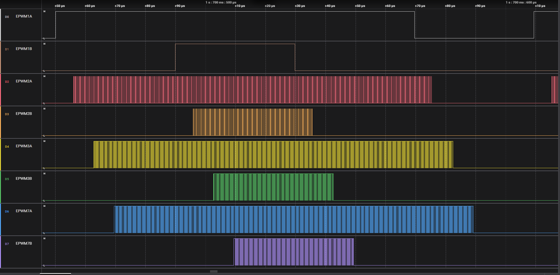
Fig. 5.70 Cdd Pwm Example Chopper Waveform
5.16.11.2. Cdd_Pwm_Example_Cmpss_Trip
5.16.11.2.1. Overview Of Cdd_Pwm_Example_Cmpss_Trip
Cdd_Pwm_Example_Cmpss_Trip (Advanced mode)
This example enables the CMPSS1 COMPH comparator and feeds the asynchronous signal CTRIPH to GPIO1/CDD_PWM1B. CMPSS is configured to trip the PWM signals.
The positive pin of the CMPSS is used to give positive input and internal DAC in CMPSS is configured to feed the negative pin. The DAC is configured to provide a signal at VDD/2.
When a low signal (VSS) is provided to positive pin of CMPSS1, PWM signal comes out on GPIO1.
When a high signal (greater than VDD/2) is provided to positive pin of CMPSS1, the PWM signal at GPIO1 trips and goes high.
Example is configured such that PWM coming at GPIO0 will remain unaffected.
DeviceSupport_Init()
Initialize FLASH if the example is run in FLASH mode
EcuM_Init()
Initialize clock to 100 MHz using Mcu_Init()
Initialize pins in CDD_PWM mode with Port_Init()
Initialize Cdd_Pwm driver using Cdd_Pwm_Init()
Configure Cdd_Pwm hardware using Cdd_Pwm_ConfigureHw()
Configure CMPSS module using Cmpss_Init()
Feed pin B0 (pin 12 on HSEC) to VSS or to a signal greater than VDD/2 to observe the behaviour
CDD_PWM waveform can be observed on the respective pins configured in CDD_PWM mode
External Connections:
GPIO0 CDD_PWM1A
GPIO1 CDD_PWM1B
Positive pin of CMPSS is at B0 pin (Pin 12 of HSEC board)
5.16.11.2.2. Setup required to run Cdd_Pwm_Example_Cmpss_Trip example
Connect the pins configured for EPWM as per the example description to the LA to observe generated waveform.
Power the board and run the example
Open serial console to observe print statements of the example
5.16.11.2.3. How to run Cdd_Pwm_Example_Cmpss_Trip example
Open CCS and import Cdd_Pwm_Example_Cmpss_Trip Example
Build project and start debug project
5.16.11.2.4. Sample Log of Cdd_Pwm_Example_Cmpss_Trip example
CDD_PWM MCAL Version Info
---------------------
Vendor ID           : 44
Module ID           : 255
SW Major Version    : 3
SW Minor Version    : 1
SW Patch Version    : 2
Number of notifications detected for CDD_PWM1 are 447929
Number of trip zone interrupts detected for CDD_PWM1 are 10
Generated waveforms can be observed on the configured CDD_PWM pins
Cdd_Pwm_Example_Cmpss_Trip example executed successfully
5.16.11.2.5. Waveform of Cdd_Pwm_Example_Cmpss_Trip example
Fig. 5.71 Cdd Pwm Example Cmpss Trip Waveform
5.16.11.3. Cdd_Pwm_Example_DC_EventFilter
5.16.11.3.1. Overview Of Cdd_Pwm_Example_DC_EventFilter
Cdd_Pwm_Example_DC_EventFilter (Advanced mode)
DeviceSupport_Init()
-Initialize FLASH if the example is run in FLASH mode
EcuM_Init()
-Initialize clock to 100 MHz using Mcu_Init()
-Initialize pins with Port_Init()
-Initialize Cdd_Pwm driver using Cdd_Pwm_Init()
Configure Cdd_Pwm hardware using Cdd_Pwm_ConfigureHw() to configure EPWM1 as follows
-EPWM1 with DCAEVT1 forcing the EPWM output LOW
-GPIO12 is used as the input to the INPUT XBAR INPUT2
-INPUT2 (from INPUT XBAR) is used as the source for DCAEVT1
-GPIO12’s PULL-UP resistor is enabled, in order to test the trip, PULL this pin to GND using Dio_WriteChanel API
-DCAEVT1 uses the filtered version of DCAEVT1
-The DCFILT signal uses the blanking window to ignore the DCAEVT1 for the duration of DC Blanking window
-EPWM1 with DCBEVT1 forcing the EPWM output LOW
-GPIO12 is used as the input to the INPUT XBAR INPUT2
-INPUT2 (from INPUT XBAR) is used as the source for DCBEVT1
-GPIO12’s PULL-UP resistor is enabled, in order to test the trip, PULL this pin to GND using Dio_WriteChanel API
DCAEVT1 & DCBEVT1 events are configured to force to LOW when the trip occurs on the TRIP2 input.
Trip input is pulled LOW which triggers LOW state on both the EPWM outputs and notifications are expected.
Blanking window is increased to test event filtering.
Trip input is pulled to LOW during the blanking window. Only EPWMB waveform should be affected by this and
0 notifications are expected.
Disable blanking window.
Trip input is pulled to LOW, both output waveforms should be affected by this and notifications are expected.
Print notification counts in sequence to track the events.
EPWM waveform can be observed on the respective pins configured in EPWM mode
\b External \b Connections \n
-GPIO0 EPWM1A
-GPIO1 EPWM1B
-GPIO12 –> TRIPIN2. This pin is pulled LOW using DIO to trip the EPWM.
5.16.11.3.2. Setup required to run Cdd_Pwm_Example_DC_EventFilter example
Connect the pins configured for EPWM as per the example description to the LA to observe generated waveform.
Power the board and run the example
Open serial console to observe print statements of the example
5.16.11.3.3. How to run Cdd_Pwm_Example_DC_EventFilter example
Open CCS and import Cdd_Pwm_Example_DC_EventFilter Example
Build project and start debug project
5.16.11.3.4. Sample Log of Cdd_Pwm_Example_DC_EventFilter example
Executing Cdd_Pwm_Example_DC_EventFilter example
CDD_PWM MCAL Version Info
---------------------
Vendor ID           : 44
Module ID           : 255
SW Major Version    : 3
SW Minor Version    : 1
SW Patch Version    : 2
Notification count is 3
Notification count after increasing the blanking window is 0
Notification count after disabling the blanking window is 3
Generated waveforms can be observed on the configured EPWM pins
Cdd_Pwm_Example_DC_EventFilter example executed successfully
5.16.11.3.5. Waveform of Cdd_Pwm_Example_DC_EventFilter example
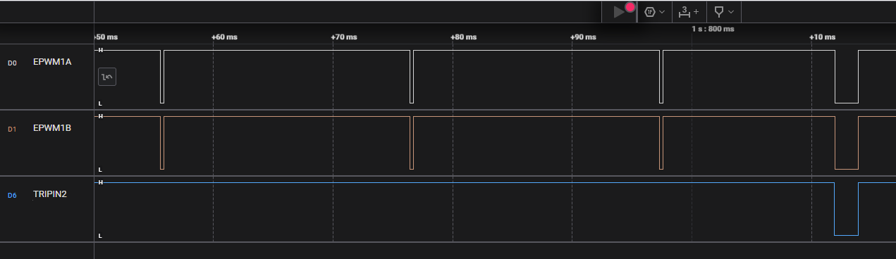
Fig. 5.72 Cdd Pwm Example DC EventFilter Waveform
5.16.11.4. Cdd_Pwm_Example_Deadband
5.16.11.4.1. Overview Of Cdd_Pwm_Example_Deadband
Cdd_Pwm_Example_Deadband (Advanced mode)
DeviceSupport_Init()
-Initialize FLASH if the example is run in FLASH mode
EcuM_Init()
-Initialize clock to 100 MHz using Mcu_Init()
-Initialize pins with Port_Init()
-Initialize Cdd_Pwm driver using Cdd_Pwm_Init()
Initialize EPWM instances using Cdd_Pwm_ConfigureHw()
-EPWM1 with Deadband disabled (Reference)
-EPWM2 with Deadband Active High
-EPWM3 with Deadband Active Low
-EPWM4 with Deadband Active High Complimentary
-EPWM7 with Deadband Active Low Complimentary
Track the output waveforms for 1 second and disable all notifications and interrupts.
Print the notification counts to track the notification count for each EPWM instance.
-GPIO0 EPWM1A
-GPIO1 EPWM1B
-GPIO2 EPWM2A
-GPIO3 EPWM2B
-GPIO4 EPWM3A
-GPIO5 EPWM3B
-GPIO27 EPWM4A
-GPIO28 EPWM4B
-GPIO12 EPWM7A
-GPIO13 EPWM7B
5.16.11.4.2. Setup required to run Cdd_Pwm_Example_Deadband example
Connect the pins configured for EPWM as per the example description to the LA to observe generated waveform.
Power the board and run the example
Open serial console to observe print statements of the example
5.16.11.4.3. How to run Cdd_Pwm_Example_Deadband example
Open CCS and import Cdd_Pwm_Example_Deadband Example
Build project and start debug project
5.16.11.4.4. Sample Log of Cdd_Pwm_Example_Deadband example
Executing Cdd_Pwm_Example_Deadband example
CDD_PWM MCAL Version Info
---------------------
Vendor ID           : 44
Module ID           : 255
SW Major Version    : 3
SW Minor Version    : 1
SW Patch Version    : 2
Number of interrupts detected for EPWM1 are 1000
Number of interrupts detected for EPWM2 are 4000
Number of interrupts detected for EPWM3 are 4000
Number of interrupts detected for EPWM4 are 4000
Number of interrupts detected for EPWM7 are 4000
Generated waveforms can be observed on the configured EPWM pins
Cdd_Pwm_Example_Deadband example executed successfully
5.16.11.4.5. Waveform of Cdd_Pwm_Example_Deadband example
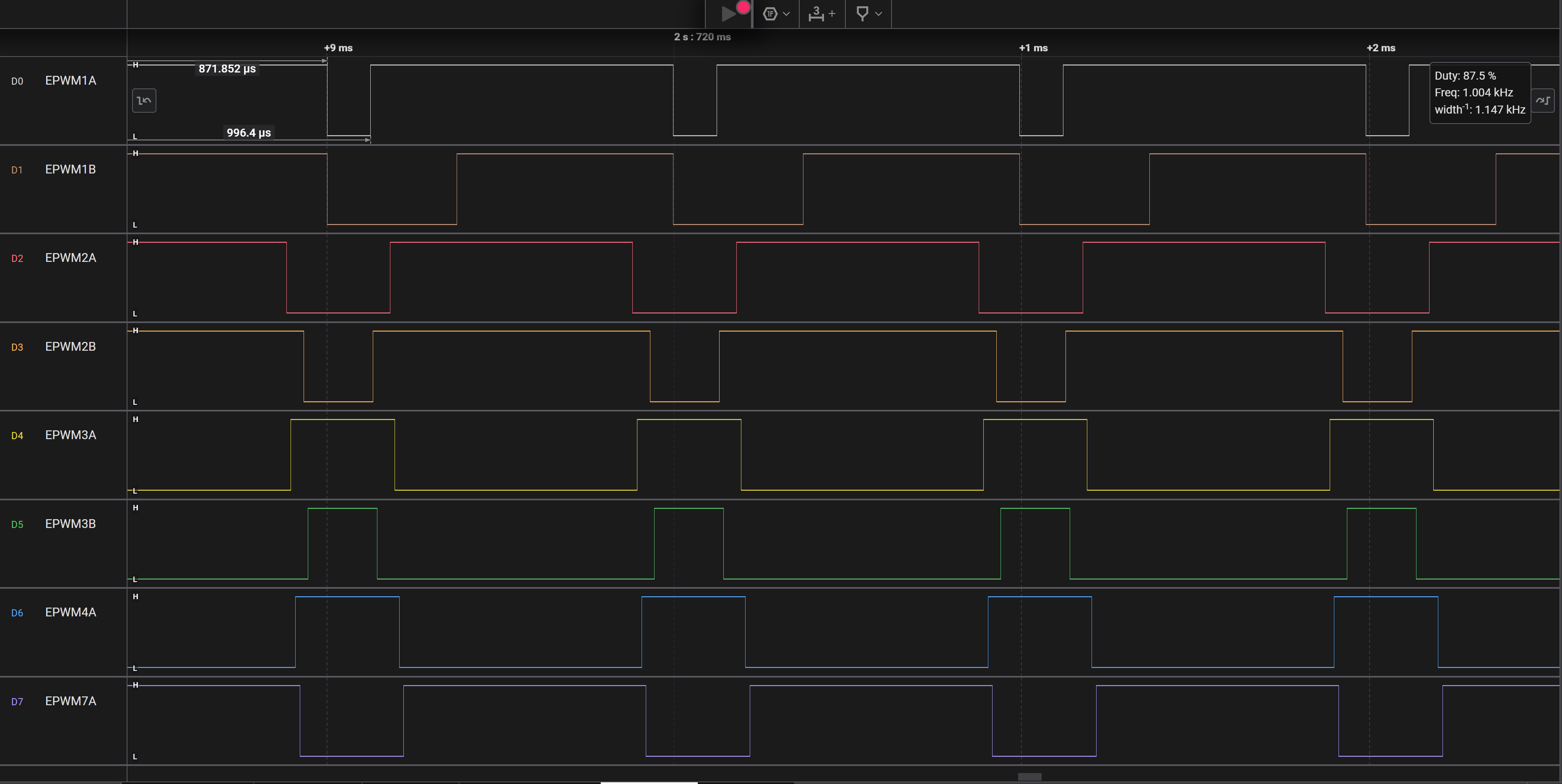
Fig. 5.73 Cdd Pwm Example Deadband Waveform
5.16.11.5. Cdd_Pwm_Example_DiodeEmulation
5.16.11.5.1. Overview Of Cdd_Pwm_Example_DiodeEmulation
Cdd_Pwm_Example_DiodeEmulation (Advanced mode)
DeviceSupport_Init()
-Initialize FLASH if the example is run in FLASH mode
EcuM_Init()
-Initialize clock to 100 MHz using Mcu_Init()
-Initialize pins with Port_Init()
-Initialize Cdd_Pwm driver using Cdd_Pwm_Init()
-Configure Cdd_Pwm hardware using Cdd_Pwm_ConfigureHw() to configure EPWM instances as follows
Diode Emulation configuration:
-For EPWM1 A & B outputs the AQ actions are configured to HIGH & LOW respectively.
And the diode emulation trip signals are set to opposite of the configured polarities respectively,
EPWM1A is set to HIGH and EPWM1B set to LOW during DE
-For EPWM2 A & B outputs the AQ actions are configured to LOW & HIGH respectively.
And the diode emulation trip signals are set to opposite of the configured polarities respectively,
EPWM2A is set to LOW and EPWM2B set to HIGH during DE
-EPWM1 & EPWM2 are configured in one-shot diode emulation mode,
Force diode emulation active flag to enter diode emulation mode
-EPWM3 is configured same as EPWM1 but in CBC(cycle-by-cycle) DE mode
Force diode emulation active flag to enter diode emulation mode
In the Cycle-by-cycle clear mode, trip condition is evaluated on every EPWMxSYNCPER and if the
trip condition is not present, then DEACTIVE flag is cleared (exiting of DE mode)
Force diode emulation active flag for both EPWM1 & EPWM2 and wait until EPWM1 & EPWM2 outputs are changed to the
configured state (EPWM1A to HIGH, EPWM1B to LOW, EPWM2A to LOW & EPWM2B to HIGH).
Clear active diode emulation flags for both EPWM1 & EPWM2 instances to exit DE mode.
Force diode emulation active flag for EPWM1
Wait until EPWM1 enters the DE mode and check if the EPWM2 has entered the DE mode.
The execution will stay in the loop if the expected condition is not achieved.
Clear active diode emulation flags for both EPWM1 to exit DE mode.
Force diode emulation active flag for EPWM3
Wait until EPWM3 outputs are changed to the configured state (EPWM3A to HIGH & EPWM3B to LOW).
Wait until the CBC clear the active flag and the EPWM instance exits the DE mode.
EPWM waveform and DE intput trip signals can be monitored on the respective pins configured
-GPIO0 EPWM1A
-GPIO1 EPWM1B
-GPIO2 EPWM2A
-GPIO3 EPWM2B
-GPIO4 EPWM3A
-GPIO5 EPWM3B
5.16.11.5.2. Setup required to run Cdd_Pwm_Example_DiodeEmulation example
Connect the pins configured for EPWM as per the example description to the LA to observe generated waveform.
Power the board and run the example
Open serial console to observe print statements of the example
5.16.11.5.3. How to run Cdd_Pwm_Example_DiodeEmulation example
Open CCS and import Cdd_Pwm_Example_DiodeEmulation Example
Build project and start debug project
5.16.11.5.4. Sample Log of Cdd_Pwm_Example_DiodeEmulation example
Executing Cdd_Pwm_Example_DiodeEmulation example
CDD_PWM MCAL Version Info
---------------------
Vendor ID           : 44
Module ID           : 255
SW Major Version    : 3
SW Minor Version    : 1
SW Patch Version    : 2
Force diode emulation active flags for EPWM1 & EPWM2 instances
EPWM1A output is HIGH
EPWM2A output is LOW
Cleared diode emulation active flags for EPWM1 & EPWM2 instances
Force diode emulation active flags for EPWM1 instance
EPWM1A output is HIGH
EPWM2A output is HIGH
Cleared diode emulation active flags for EPWM1 instance
Force diode emulation active flags for EPWM3 instance
EPWM3A output is HIGH
Diode emulation active flag has been cleared by hardware
Generated waveforms can be observed on the configured EPWM pins
Cdd_Pwm_Example_DiodeEmulation example executed successfully
5.16.11.5.5. Waveform of Cdd_Pwm_Example_DiodeEmulation example
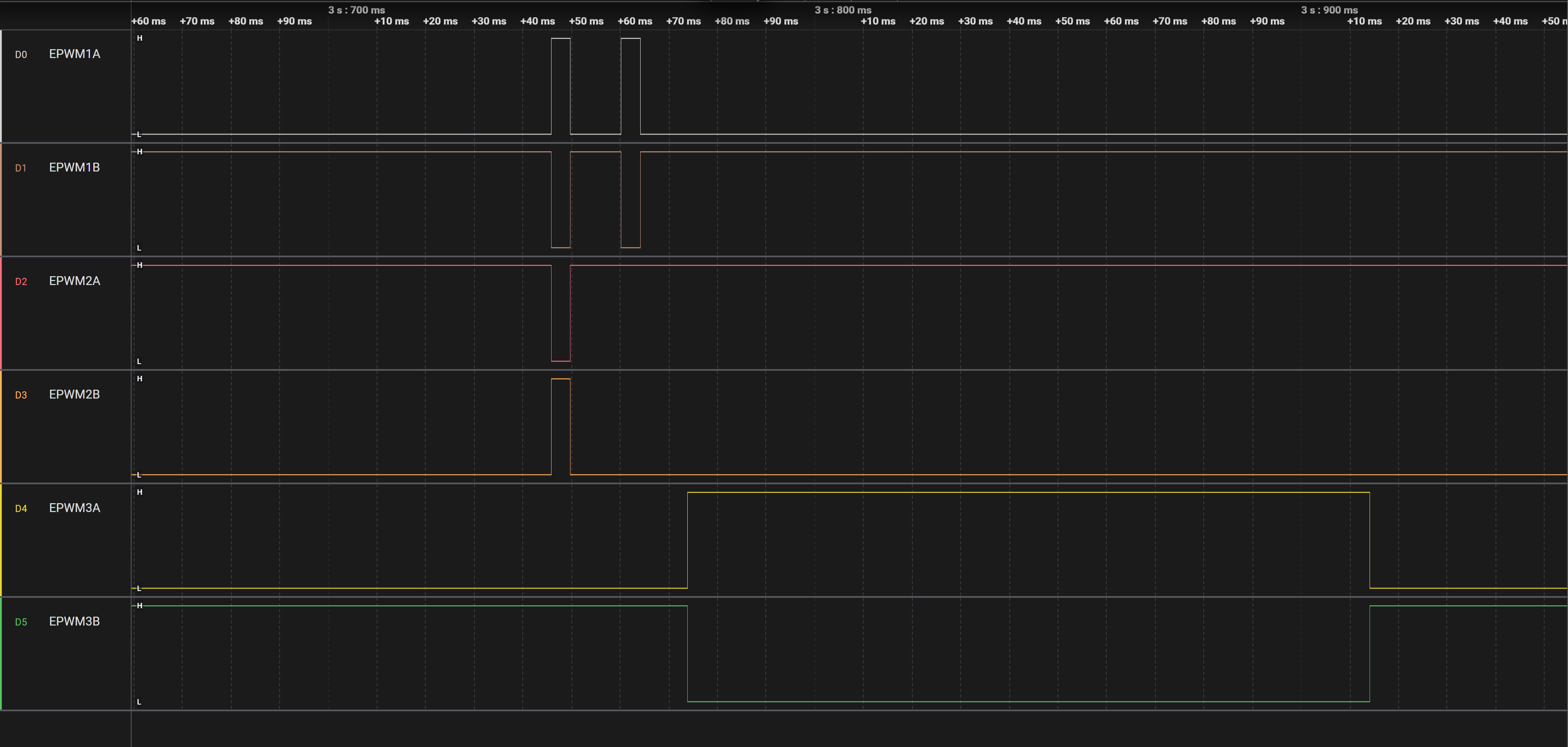
Fig. 5.74 Cdd Pwm Example DiodeEmulation Waveform
5.16.11.6. Cdd_Pwm_Example_GlobalLoad_And_Link
5.16.11.6.1. Overview Of Cdd_Pwm_Example_GlobalLoad_And_Link
Cdd_Pwm_Example_GlobalLoad_And_Link (Advanced mode)
DeviceSupport_Init()
-Initialize FLASH if the example is run in FLASH mode
EcuM_Init()
-Initialize clock to 100 MHz using Mcu_Init()
-Initialize pins with Port_Init()
-Initialize Cdd_Pwm driver using Cdd_Pwm_Init() to enable XLINK for the EPWM instances
-Cdd_Pwm_ConfigureHw() as follows
-For EPWM1 enable notification and linking
-For EPWM2 enable global load and linking. TBCTR = Period is the configured global load trigger and the event
prescale is configured to 7.
-For EPWM3 enable linking
-For EPWM7 enable linking
-Configure prescaler, compare values and action qualifier actions using linking
Laod a period value to all EPWM instances using XLINK. This period value results in 50% duty cycle for all the
EPWM OUTPUT A channels.
Counter compare values are updated at 3rd period event for EPWM 1 & 2 instances. The configured
global load event prescale is 7. So, the update in the compare compare values(shadow to active at 3rd period event)
can be observed in only EPWM1 instances.
Update in the compare compare values(shadow to active at 7rd period event) can be observed in both EPWM1 & EPWM2 instances.
As a result, the duty cycle of the EPWM1 instance will jump from 50% to 25% and then to 25%.
But EPWM2 instance will jump from 50% to 20% while EPWM3 & EPWM7 instances maintain their duty cycles at 50%.
Wait for 1 second and update the compare B value for all the EPWM instances using linking.
With the latest compare B value, the duty cycle of EPWM3 & EPWM7’s OUTPUT A will jump to 75%.
Duty cycle of EPWM1 & EPWM2’s channel A will jump to 75%.
Print the notification count to of all EPWM instances.
-GPIO0 EPWM1A
-GPIO2 EPWM2A
-GPIO4 EPWM3A
-GPIO27 EPWM4A
5.16.11.6.2. Setup required to run Cdd_Pwm_Example_GlobalLoad_And_Link example
Connect the pins configured for EPWM as per the example description to the LA to observe generated waveform.
Power the board and run the example
Open serial console to observe print statements of the example
5.16.11.6.3. How to run Cdd_Pwm_Example_GlobalLoad_And_Link example
Open CCS and import Cdd_Pwm_Example_GlobalLoad_And_Link Example
Build project and start debug project
5.16.11.6.4. Sample Log of Cdd_Pwm_Example_GlobalLoad_And_Link example
Executing Cdd_Pwm_Example_GlobalLoad_And_Link example
CDD_PWM MCAL Version Info
---------------------
Vendor ID           : 44
Module ID           : 255
SW Major Version    : 3
SW Minor Version    : 1
SW Patch Version    : 2
Load period to the xlink region
Load new compare A value to the both EPWM1 & EPWM2 instances
Load new compare B value to the both EPWM1 & EPWM2 instances
Load new compare B value to the xlink region
Notification count for the EPWM1 instance is 100
Generated waveforms can be observed on the configured EPWM pins
Cdd_Pwm_Example_GlobalLoad_And_Link example executed successfully
5.16.11.6.5. Waveform of Cdd_Pwm_Example_GlobalLoad_And_Link example
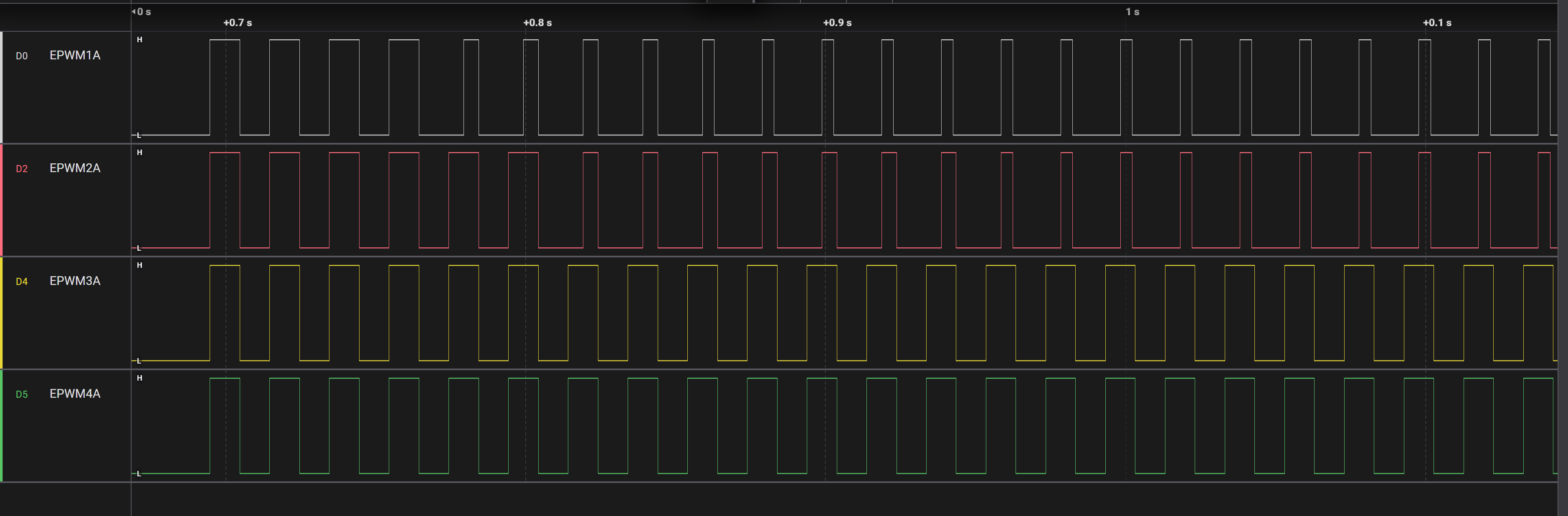
Fig. 5.75 Cdd Pwm Example GlobalLoad And Link Waveform
5.16.11.7. Cdd_Pwm_Example_Hrpwm
5.16.11.7.1. Overview Of Cdd_Pwm_Example_Hrpwm
Cdd_Pwm_Example_Hrpwm (Advanced mode)
DeviceSupport_Init()
Initialize FLASH if the example is run in FLASH mode
EcuM_Init()
Initialize clock to 100 MHz using Mcu_Init()
Initialize pins with Port_Init()
Initialize Cdd_Pwm driver using Cdd_Pwm_Init()
Configure Cdd_Pwm hardware using Cdd_Pwm_ConfigureHw() as follows
EPWM1 with HRPWM disabled(for reference)
EPWM2 with HRPWM enabled (for both A & B channels MEP edge is configured as FALLING EDGE)
Print the notification count of all EPWM instances.
EPWM waveform can be observed on the respective pins configured in EPWM mode
GPIO0 EPWM1A
GPIO1 EPWM1B
GPIO2 EPWM2A
GPIO3 EPWM2B
5.16.11.7.2. Setup required to run Cdd_Pwm_Example_Hrpwm example
Connect the pins configured for EPWM as per the example description to the LA to observe generated waveform.
Power the board and run the example
Open serial console to observe print statements of the example
5.16.11.7.3. How to run Cdd_Pwm_Example_Hrpwm example
Open CCS and import Cdd_Pwm_Example_Hrpwm Example
Build project and start debug project
5.16.11.7.4. Sample Log of Cdd_Pwm_Example_Hrpwm example
Executing Cdd_Pwm_Example_Hrpwm example
CDD_PWM MCAL Version Info
---------------------
Vendor ID           : 44
Module ID           : 255
SW Major Version    : 3
SW Minor Version    : 1
SW Patch Version    : 2
EPWM1 instance is operating in normal PWM mode
EPWM2 instance is operating in high-resolution mode
Increment the duty cycle by 0.01% percent for every iteration from 4% to 99.99%
Number of rising edges detected for EPWM2 are 1117848
Waveforms can be observed on the configured EPWM pins
Cdd_Pwm_Example_Hrpwm example executed successfully
5.16.11.7.5. Waveform of Cdd_Pwm_Example_Hrpwm example
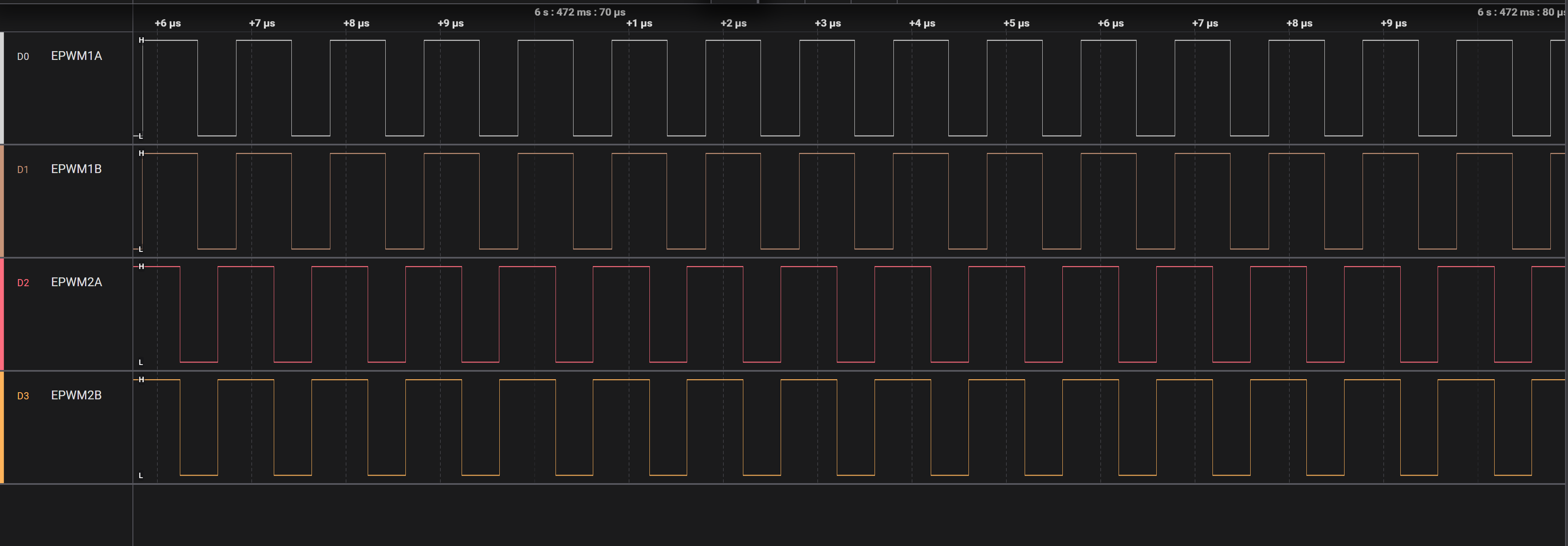
Fig. 5.76 Cdd Pwm Example Hrpwm Waveform
5.16.11.8. Cdd_Pwm_Example_TripZone
5.16.11.8.1. Overview Of Cdd_Pwm_Example_TripZone
Cdd_Pwm_Example_TripZone (Advanced mode)
DeviceSupport_Init()
-Initialize FLASH if the example is run in FLASH mode
EcuM_Init()
-Initialize clock to 100 MHz using Mcu_Init()
-Initialize pins with Port_Init()
-Initialize Cdd_Pwm driver using Cdd_Pwm_Init()
Configure Cdd_Pwm hardware using Cdd_Pwm_ConfigureHw() to configure EPWM1 as follows
-EPWM1 with no trip zone configuration (reference)
-EPWM2 with trip zone enabled in one-shot mode
-EPWM3 with trip zone enabled in CBC(cycle-by-cycle) mode
Pull Dio channel(GPIO 12) to LOW to trip the EPWM2 & EPWM3 instances
EPWM2 is configured in one-shot mode so the flags must be cleared manually but for EPWM3 which is in CBC the flags are automatically cleared at the end of the cycle if the trip condition doesn’t apply anymore.
Pull back the Dio channel(GPIO 12) to HIGH to resume the normal operation
The change in the output waveforms can be tracked with a logic analyzer
-EPWM1A is on GPIO0
-EPWM2A is on GPIO2
-EPWM3B is on GPIO5
-TZ1 is on GPIO12 and is linked to Dio Channel 0
This example also makes use of the Input X-BAR. GPIO12 (the external trigger) is routed to the input X-BAR, from which it is routed to TZ1.
The TZ-Event is defined such that EPWM1 will undergo a One-Shot Trip and EPWM2 will undergo a Cycle-By-Cycle Trip.
             _____________             __________________
             |           |             |                |
 GPIO12 -----| I/P X-BAR |-----TZ1-----| EPWM TZ Module |-----TZ-Event
             |___________|             |________________|
5.16.11.8.2. Setup required to run Cdd_Pwm_Example_TripZone example
Connect the pins configured for EPWM as per the example description to the LA to observe generated waveform.
Connect a switch to the configured trip zone input pin.
Power the board and run the example
Open serial console to observe print statements of the example
5.16.11.8.3. How to run Cdd_Pwm_Example_TripZone example
Open CCS and import Cdd_Pwm_Example_TripZone Example
Build project and start debug project
5.16.11.8.4. Sample Log of Cdd_Pwm_Example_TripZone example
Executing Cdd_Pwm_Example_TripZone example
Number of trip zone interrupts detected for EPWM2 before trip are 0
Number of trip zone interrupts detected for EPWM2 are 3
Waveforms can be observed on the configured EPWM pins
Cdd_Pwm_Example_TripZone example executed successfully
5.16.11.8.5. Waveform of Cdd_Pwm_Example_TripZone example
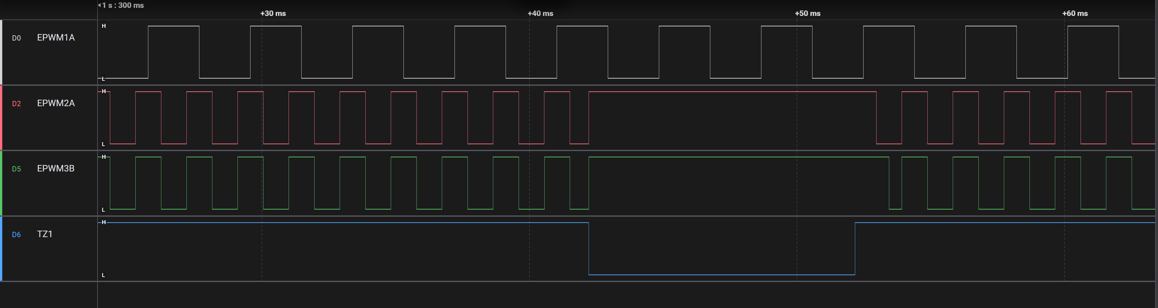
Fig. 5.77 Cdd Pwm Example TripZone Waveform
5.16.11.9. Cdd_Pwm_Example_UpCountMode
5.16.11.9.1. Overview Of Cdd_Pwm_Example_UpCountMode
Cdd_Pwm_Example_UpCountMode (Simple mode)
DeviceSupport_Init()
-Initialize FLASH if the example is run in FLASH mode
EcuM_Init()
-Initialize clock to 100 MHz using Mcu_Init()
-Initialize pins with Port_Init()
-Initialize Cdd_Pwm driver using Cdd_Pwm_Init()
Enable channel A rising edge notifications for both the PWM instances
Set the all the outputs to IDLE with Cdd_Pwm_SetOutputToIdle API
Activate the channels and change the duty cycle of the waveform with Cdd_Pwm_SetDutyCycle() API
and observe the change in the generated PWM output waveform Set PWM1 outputs to IDLE with
Cdd_Pwm_SetOutputToIdle API Activate the channels & period of the channels associated to PWM1
instance with Cdd_Pwm_SetPeriod() API and observe the change in the frequency of the generated output waveforms
EPWM waveform can be observed on the respective pins configured in EPWM mode
-GPIO0 EPWM1A
-GPIO1 EPWM1B
-GPIO2 EPWM2A
-GPIO3 EPWM2B
5.16.11.9.2. Setup required to run Cdd_Pwm_Example_UpCountMode example
Connect the pins configured for EPWM as per the example description to the LA to observe generated waveform.
Power the board and run the example
Open serial console to observe print statements of the example
5.16.11.9.3. How to run Cdd_Pwm_Example_UpCountMode example
Open CCS and import Cdd_Pwm_standard Example
Build project and start debug project
5.16.11.9.4. Sample Log of Cdd_Pwm_Example_UpCountMode example
Executing Cdd_Pwm_Example_UpCountMode example
The duty cycles of the EPWM1 & EPWM2 channels have been modified
The notification count for EPWM1 instance after calling Cdd_Pwm_SetDutyCycle API is 120
The notification count for EPWM2 instance after calling Cdd_Pwm_SetDutyCycle API is 2428
All the EPWM1 & EPWM2 channels in IDLE state
The notification count for EPWM1 instance after calling Cdd_Pwm_SetDutyCycle API is 122
The notification count for EPWM2 instance after calling Cdd_Pwm_SetDutyCycle API is 2444
The frequency of EPWM1 has been doubled(period halved)
The duty cycle of the EPWM2 channels have been modified
Time elapsed in US(microsecond) from when the notification is enabled until Deinit is 3452090
Number of rising edges detected for EPWM1 are 322
Number of edges detected for EPWM2 are 4465
Waveforms can be observed on the configured EPWM pins
Cdd_Pwm_Example_UpCountMode executed successfully
5.16.11.9.5. Waveform of Cdd_Pwm_Example_UpCountMode example
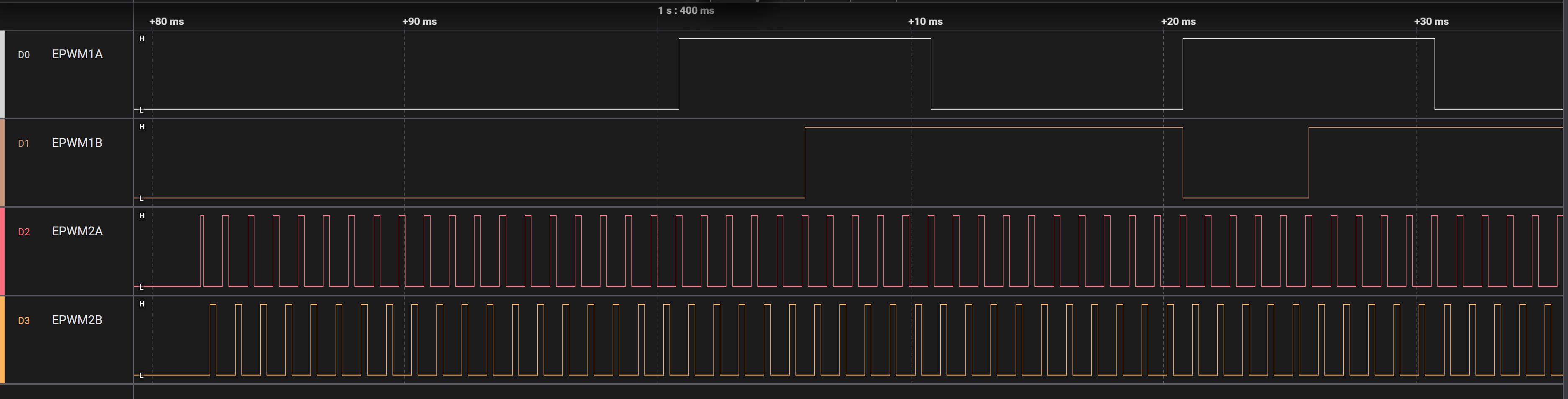
Fig. 5.78 Cdd Pwm Example UpCountMode Waveform
5.16.11.10. Cdd_Pwm_Example_XCmp_MultipleEdges
5.16.11.10.1. Overview Of Cdd_Pwm_Example_XCmp_MultipleEdges
Cdd_Pwm_Example_XCmp_MultipleEdges (Advanced mode)
DeviceSupport_Init()
-Initialize FLASH if the example is run in FLASH mode
EcuM_Init()
-Initialize clock to 100 MHz using Mcu_Init()
-Initialize pins with Port_Init()
-Initialize Cdd_Pwm driver using Cdd_Pwm_Init()
Configure Cdd_Pwm hardware using Cdd_Pwm_ConfigureHw() as follows
-EPWM1A is allocated all XCMP1-8 registers. EPWM1B has no output.
-No Shadow registers used
-EPWM2A is allocated XCMP1-4 and EPWM2B is allocated XCMP5-8 registers.
-Configured in LOAD ONCE mode and the XCMP values are updated every period with a new shadow buffer set
-Shadow level is set to 3
-EPWM3A is allocated XCMP1-4 and EPWM2B is allocated XCMP5-8 registers.
-Configured in LOAD MULTIPLE mode. Repeat count is configured for SHD buffer set 3 & 2.
The SHDBUF ptr is set to 3 again after 16 periods.
-Shadow level is set to 3
EnableXLoad trigger the XCMP mode
Print the notification count for each EPWM instance
Track the changes in the waveforn with a logic analyzer
EPWM waveform can be observed on the respective pins configured in EPWM mode
-GPIO0 EPWM1A
-GPIO1 EPWM1B
-GPIO2 EPWM2A
-GPIO3 EPWM2B
-GPIO4 EPWM3A
-GPIO5 EPWM3B
5.16.11.10.2. Setup required to run Cdd_Pwm_Example_XCmp_MultipleEdges example
Connect the pins configured for EPWM as per the example description to the LA to observe generated waveform.
Power the board and run the example
Open serial console to observe print statements of the example
5.16.11.10.3. How to run Cdd_Pwm_Example_XCmp_MultipleEdges example
Open CCS and import Cdd_Pwm_Example_XCmp_MultipleEdges Example
Build project and start debug project
5.16.11.10.4. Sample Log of Cdd_Pwm_Example_XCmp_MultipleEdges example
Executing Cdd_Pwm_Example_XCmp_MultipleEdges example
EPWM1 has split XCMP disabled
EPWM2 is set to LOAD ONCE XCMP mode
EPWM3 is set to LOAD MULTIPLE XCMP mode
Enable XCMP load for all EPWM instances
Number of interrupts detected for EPWM2 are 2000
Number of interrupts detected for EPWM3 are 2000
Waveforms can be observed on the configured EPWM pins
Cdd_Pwm_Example_XCmp_MultipleEdges example executed successfully
5.16.11.10.5. Waveform of Cdd_Pwm_Example_XCmp_MultipleEdges example
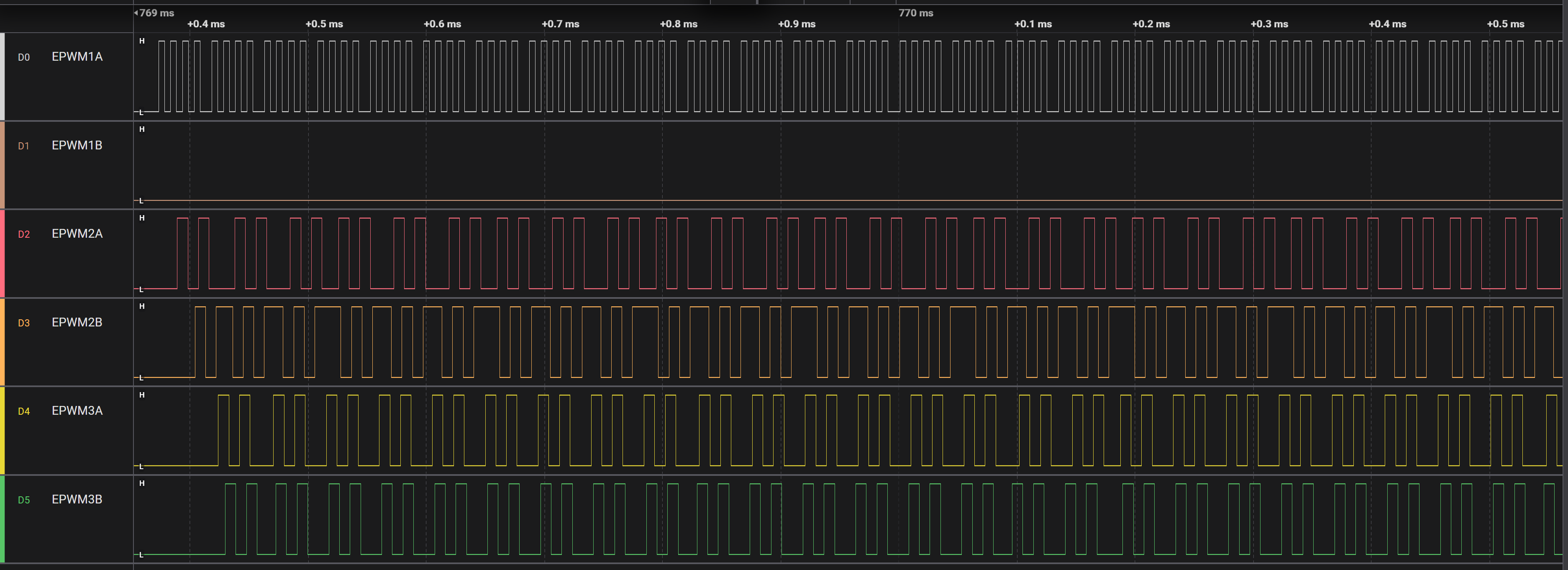
Fig. 5.79 Cdd Pwm Example XCmp MultipleEdges Waveform
5.16.11.11. File Structure
📦f29h85x_mcal
┣ 📂build
┣ 📂docs
┣ 📂drivers
┣ 📂examples
┃ ┣ 📂AppUtils
┃ ┣ 📂Can
┃ ┣ 📂Cdd_Adc
┃ ┣ 📂Cdd_Ecap
┃ ┣ 📂Cdd_Ipc
┃ ┣ 📂Cdd_Pwm
┃ ┃ ┣ 📂Cdd_Pwm_Example_UpCountMode
┃ ┃ ┃ ┣ 📂CCS
┃ ┃ ┃ ┃ ┗ 📜Cdd_Pwm_Example_UpCountMode.projectspec
┃ ┃ ┃ ┣ Cdd_Pwm_Example_UpCountMode_Config
┃ ┃ ┃ ┃ ┣ 📂config
┃ ┃ ┃ ┃ ┃ ┣ 📜Cdd_Pwm.xdm : Generated EB Tresos config file in .xdm format
┃ ┃ ┃ ┃ ┃ ┣ 📜Dem.xdm
┃ ┃ ┃ ┃ ┃ ┣ 📜EcuM.xdm
┃ ┃ ┃ ┃ ┃ ┣ 📜Mcu.xdm
┃ ┃ ┃ ┃ ┃ ┣ 📜Os.xdm
┃ ┃ ┃ ┃ ┃ ┗ 📜Port.xdm
┃ ┃ ┃ ┃ ┣ 📂include
┃ ┃ ┃ ┃ ┃ ┣ 📜Cdd_Pwm_Cfg.h : Contains the generated pre-compiler build variant configuration header file
┃ ┃ ┃ ┃ ┃ ┣ 📜Dem_Cfg.h
┃ ┃ ┃ ┃ ┃ ┣ 📜EcuM_Cfg.h
┃ ┃ ┃ ┃ ┃ ┣ 📜Mcu_Cfg.h
┃ ┃ ┃ ┃ ┃ ┣ 📜Os_Cfg.h
┃ ┃ ┃ ┃ ┃ ┗ 📜Port_Cfg.h
┃ ┃ ┃ ┃ ┣ 📂src
┃ ┃ ┃ ┃ ┃ ┣ 📜Cdd_Pwm_Cfg.c : Contains the Pre-compile build variant configuration parameters.
┃ ┃ ┃ ┃ ┃ ┣ 📜Dem_Cfg.c
┃ ┃ ┃ ┃ ┃ ┣ 📜EcuM_Cfg.c
┃ ┃ ┃ ┃ ┃ ┣ 📜Mcu_PBcfg.c
┃ ┃ ┃ ┃ ┃ ┣ 📜Os_Cfg.c
┃ ┃ ┃ ┃ ┃ ┗ 📜Port_PBcfg.c
┃ ┃ ┃ ┃ ┗ 📜CMakeLists.txt
┃ ┃ ┃ ┣ 📜Cdd_Pwm_Example_UpCountMode.c : Example application for Cdd_Pwm.
┃ ┃ ┃ ┗ 📜CMakeLists.txt
┃ ┣ 📂Cdd_Sent
┃ ┣ 📂Cdd_Uart
┃ ┣ 📂Cdd_Xbar
┃ ┣ 📂DeviceSupport
┃ ┣ 📂Dio
┃ ┣ 📂Gpt
┃ ┣ 📂Lin
┃ ┣ 📂Mcu
┃ ┣ 📂Port
┃ ┣ 📂Spi
┃ ┣ 📂Wdg
┣ 📂plugins
┣ 📜CMakeLists.txt
┗ 📜CMakePresets.json