Design Guide
Introduction
Capacitive touch detection is sometimes considered more art than science. This often results in multiple design iterations before the optimum performance is achieved. There are, however, good design practices for circuit layout and principles of materials that need to be understood to keep the number of iterations to a minimum.
Good sensor design are the foundation for a successful touch product.
The purpose of this design guide is to provide guidance for the design and layout of capacitive touch sensors so that they can achieve maximum performance. By achieving maximum performance in the hardware, the CapTIvate™ capacitive touch software library can perform the capacitive touch measurements consuming the lowest power. Tuning guides, along with the CapTIvate™ Design Center are used to help tune the performance of the capacitive touch application.
Starting a New Design
Starting any new capacitive touch design can be a challenging task. This section will guide you through this process and help determine what is important for your design and end application.
Identify Sensors
First we want to identify the types of sensors that you are considering for your application and provide some basic design guidelines.
Identify Care Abouts
Next it is important to identify any special requirements for the end application, such as low-power, noise immunity, moisture, etc.
Design Process
Creating a reliable capacitive touch design can be a time consuming process that starts with designing sensors, laying out a PCB, writing lots of code and finally performing an iterative sensor tuning process to achieve the desired performance. The CapTIvate™ Technology sensor design process accelerates the capacitive touch development cycle through automation, helping get your product to market faster.
Creating a new sensor design
We begin the process by creating a new capacitive touch design using the CapTIvate™ Design Center. With a few simple drag-n-drop inputs and configuration selections, the CapTIvate™ Design Center will automatically determine the optimal pin assignments between the target MCU and the sensors (CapTIvate™ Technology peripheral can measure four channels in parallel). Alternatively, connections can be manually assigned or reserved for those applications with specific routing requirements.
Layout PCB
Once the pin assignments have been made, the MCU pin to sensor electrode connection information is exported to a .csv file and can be used during the PCB layout and design.
Generate configuration and starter project files
Now we are ready to create a custom starter code project based on our sensor design. The CapTIvate™ Design Center creates a fully working capacitive touch application that can be imported into Texas Instruments Code Composer Studio (CCS) or IAR Embedded Workbench. In addition to the application, the CapTIvate™ Software Library and MSP430 driver-lib are automatically included with the project, as portions of the libraries are needed during the development cycle.
Program target MCU
Import the generated CapTIvate™ project into Code Composer Studio or IAR IDE, compile and program the target MCU. The specific steps to perform the programming operation depend on the IDE, however, once the target MCU is programed, you are ready to start running your first capacitive touch application without having to write a single line of code!
Didn’t get it right the first time? Changes to a sensor design is simple. We use the CapTIvate™ Design Center to modify our sensor design project, then generate an updated configuration file. Simply copy the new configuration file and replace the existing one in the CCS or IAR application project and rebuild the application. That’s it!
Tune Sensors
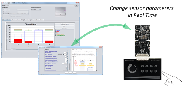
Our PCB is ready to go so we can now begin the process of tuning the sensors for the desired touch and feel. With the MCU programmed with our application and running, the sensors are scanned and real-time data is transmitted to the CapTIvate™ Design Center using the high-speed HID serial bridge MCU on the CAPTIVATE-PGMR PCB. The CapTIvate™ Design Center has several different views to display and monitor the sensor response and allow quick modifications in real-time to the sensor’s parameters, providing instant feedback.
Measure SNR and Design Margins
Now that a first-pass tuning has been created, TI recommends assessing the reliability of each sensor by utilizing the SNR measurement tool in the CapTIvate Design Center to measure the SNR and design margins. For details on this process, see the application report Sensitivity, SNR, and Design Margin in Capacitive Touch Applications.
Generate final configuration
Once our desired touch and feel is achieved, the final sensor configuration can be generated and then programmed into the target MCU. That’s it! Using the steps outlined above, capacitive sensor design time can be dramatically reduced.
Congratulations! You are done with your design and ready to go to market.
Best Practices
In this section we will cover both mechanical as well as common layout practices.
Capacitive touch detection is a type of analog-to-digital converter (ADC), specifically a capacitance-to- digital converter. As with most ADCs, the terms of interest are resolution, signal-to-noise ratio (SNR), and linearity, in the specific cases of wheels and sliders. Throughout this document, the design guidance helps to maximize signal, minimize noise, and address when these two goals are at odds.
As mentioned above, the basis of capacitive touch detection is the ability to measure a change in capacitance. This change in capacitance is the signal that the capacitive touch solution identifies. The term sensitivity is often used to describe the signal strength a more sensitive solution has a stronger signal.
Sensitivity is measured in capacitance per counts. In the context of capacitive touch detection, the magnitude of change introduced by a touch is on the order of picofarads or hundreds of femtofarads. It is not uncommon for a solution to see a touch introduce 1 pF of change and be measured as 300 counts. And while the sensitivity might be 3.3 fF/count, this should not be considered until the noise is factored in. Refer to the section on Noise below.
Sensitivity can be controlled within firmware, but the goal is to provide good sensitivity with the hardware, so that the lowest sensitivity settings can be used in firmware, which provides the lowest-power solution. Referring to the Equivalent circuit for a self capacitive sensor, C_touch must be maximized, while the other four capacitances must be minimized. The capacitances of the trace and electrode are approximated as parallel plate capacitances. The following equation serves as the basis for layout recommendations.
C = Er x E0 x A/d (1)
The dielectric constant (Er), area (A), and distance (d) are described throughout this document with the intent of positively influencing the capacitance for a touch system.
Although parasitic capacitance is presented separately, it is a part of the sensitivity and signal. As already mentioned, the capacitance of interest is the relative change in capacitance. The change in capacitance is based upon the touch interaction, but this change is perceived relative to the parasitic capacitance of the system. The parasitic capacitance is also called the steady-state capacitance or baseline capacitance. If the introduced change is 100 fF, then the sensitivity, which is the relative change in capacitance, can be increased by decreasing the parasitic capacitance.
The capacitances C_trace, C_electrode, and C_parasitics are generically referred to as parasitic capacitance.
Mechanicals
The mechanicals are the mechanical characteristics of the design. The mechanicals include the overlay material, ink on top of the overlay, any adhesives used to bond the electrode to the overlay or enclosure, and any transition materials used to remove air gaps between the electrode and the overlay. Mechanicals also include the types of materials used for the electrodes. The mechanicals affect both the signal and the parasitic capacitance.
The goal of this section is threefold:
To understand the benefits in terms of both aesthetics and robustness
To understand how the materials on top of the electrode and the electrode material itself influence the layout of the electrodes
To avoid mistakes in the mechanicals that are detrimental to the electrical performance
Typical Stackup
The following figure shows a typical stackup for a capacitive touch solution. One of the main goals of this stackup is to reduce (or eliminate, if possible) any low-dielectric (air) gaps between the electrode and the area where the touch takes place. The capacitance associated with the stackup has a very strong effect on the signal (change in capacitance from a touch). The signal is directly proportional to the dielectric of the materials. If possible, high-dielectric materials should be used, but at a minimum the stackup should eliminate any air gaps.
Air gaps can also contain moisture, which can influence performance or even damage the stackup as temperatures vary and the contents of the gap expand and contract.
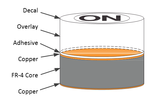
Fig. 2 Typical Material Stackup
Another critical attribute of the stackup is that it should be non-conductive. This is not usually a problem with the overlay material but can be overlooked when choosing adhesives, labels, or inks. Popular adhesives for capacitive touch solutions include 200MP products from 3M™ such as 467MP and 468MP.
Overlay
Why you want to have an Overlay?
Overlays are very important part of the capacitive touch system, it allows the designers to give their product a sleek industrial design and also provide the ESD and environment protections like the pictures showing below.
Fig. 3 Overlay Purpose
What is the trade-off?
It provides many benefits to product designers by adding an overlay on top of the capacitive sensor however the benefits come with a trade-off. When an overlay is placed between a sensor and the point of contact for a finger, a sensor’s sensitivity is greatly reduced because the overlay reduces the effective electric field going out from the sensor. The dielectric constants determines how efficiently electric Field passes through material and the distance between the overlay and the sensor determines how much electric field left in target point of contact area.
As the diagrams show below, adding an overlay over a sensor reduce the electric field going out from the sensor which reduces the strength or range of a sensor to a touch condition.
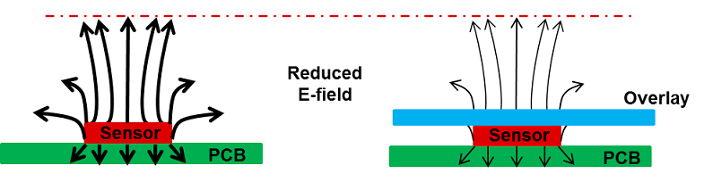
Fig. 4 Overlay Trade-off
The following figure shows the relationship between the thickness of the overlay and the sensitivity of the circuit. From the parallel plate capacitance equation, the capacitance in inversely proportional to the material thickness (C ~ 1/d).
Fig. 5 Sensitivity vs Thickness
The thickness and dielectric of the material influence the electrode design. The electrode area is a function of the area of interaction (a fingertip or the palm of the hand) while the spacing (to adjacent electrodes or ground fill) is related to the thickness of the overlay. For example, with a 2-mm overlay that has a dielectric of 3, the spacing should be approximately 1 mm (half of the thickness). Using a higher dielectric material (for example, Er = 6) the thickness could be doubled while maintaining the same level of performance. The following table shows dielectric values for various materials used as overlays.
Material |
Dielectric Constant (Er) (1) |
Breakdown Voltage (V/mm) |
|---|---|---|
Air |
1.0 |
3300 (STP) |
FR-4 |
4.8 |
20000 |
Glass |
7.6 to 8.0 |
7900 |
Gorilla® Glass |
7.2 to 7.6 |
See Manufacturer (2) |
Polycarbonate |
2.9 to 3.0 |
16000 |
Acrylic |
2.8 |
13000 |
ABS |
2.4 to 4.1 |
16000 |
Table: Material Dielectric and Breakdown Voltage
Relative permittivity
The table above also includes the breakdown voltage for different overlay materials. This should be considered when designed for ESD protection. ESD solutions should be system solutions, and any additional components should complement the protection provided by the overlay.
Electrode and Trace Materials
The performance is affected by the conductive materials that are used for the electrode and for the trace between the electrode and the microcontroller. Most applications use copper on a PCB, and copper has a resistivity of 1.7x10⁻⁶ Ohm-cm (1). As the resistivity of the conductor increases, the ability to move charge to and from the electrode decreases. This has the same effect as an increase in parasitic capacitance. This increase in resistivity, like an increase in parasitic capacitance, reduces the system sensitivity. The table below shows the resistivity for materials that are commonly used in touch applications.
Material |
Resistivity, p (Ohm-cm)(1) |
|---|---|
Copper |
1.68x10⁻⁶ |
Silver |
1.59x10⁻⁶ |
Tin |
1.09x10⁻⁵ |
Indium Tin Oxide |
1.05x10⁻³ (2) |
Table: Resistivity of Materials
Resistivity is given in Ohm-cm so that resistance is equal to the resistivity times the length divided by the cross-sectional area : R = p x L / A.
This resistivity is for a film thickness of 270 nm. Typically, vendors provide sheet resistance instead of resistivity for ITO, which is on the order of 10 to 100 Ohms per square.
When using high-resistivity materials, generally the recommendation is to increase the area of traces to reduce the resistance (at the cost of capacitance). ITO solutions provide lower sensitivity, which must be compensated for in the capacitance measurement algorithm by longer measurement times.
Other Situations
Not all applications fit into the typical category, and this section describes two special cases. The first is intentional air gaps that are greater than 2 mm between the electrode and the overlay material, and the second is the use of gloves.
Gaps
Why you want to have a gap?
In some applications, components are on the same layer as the electrode. This prevents the overlay from being directly applied to the electrode. A common example of this is when an LCD is mounted near the electrode (see diagram below). Another scenario is when the overlay material is not a uniform surface and, therefore, the electrode cannot make direct contact with the overlay.
Fig. 6 Intentional Gaps Between Electrode and Overlay
What is the trade-off?
As we discussed in the Overlay section, air has really low dielectric constant and therefore does not pass the electric field very efficiently.
As the diagram shows, theoretically the sensitivity for 1mm air gap without any moisture will be similar to an 8mm thick glass. Typical dielectric values for Air is 1. (Without moisture) Typical dielectric values for Glass is 8.
Fig. 7 Gap dielectric values
To keep the air gap without affecting too much of the sensor performance, we must bridge the gap for the sensor area with a non-conductive filler (typically adhesive) or a conductive extension. When the gap is in excess of 2 mm, then a conductive extension, either foam or metal, should be used. The metal or foam must be malleable to conform to the shape of the surfaces and prevent the formation of gaps.
When customer choice their bridge materials please take in consideration of dielectric values, transparency, mechanical support, manufacture cost, noise tolerance. The diagram below shows several materials we experimented to help to bridge the air gap and the sensitivity increase goes to an order of: Metal Spring > Conductive Foam > Carbon Fiber > Polycarbonate > ABS > Silicone
Fig. 8 Gap Bridge
In either case, the gap must be filled or bridged with a non-conductive filler (typically adhesive) or a conductive extension. When the gap is in excess of 2 mm, then a conductive extension, either foam or metal, should be used. The metal or foam must be malleable to conform to the shape of the surfaces and prevent the formation of gaps. As shown in the Figure above, the area created by the foam or metal in contact with the overlay is now the area that influences the capacitance.
Gloves
Gloves are simply another layer of medium between the electrode and the finger, and the same principles of thickness and dielectric apply. The challenges with glove applications include the ability to support both gloved and ungloved hands as well as the variation in the types of gloves the application might require. Typical leather or plastic gloves have a dielectric constant in the range of 2 to 4, and fabric gloves and gloves with insulation can have a dielectric constant less than 2.
Common Layout Considerations
After the mechanicals are understood, the electrodes can be sized and designed to provide the most signal. Independent of the mechanicals, the layout design is affected by the distance between the microcontroller and the electrodes, the PCB stackup (for example, one layer, two layer, or four layer), and other electrical circuits on the PCB.
The first item to consider relates to the schematic and the placement of any external components that are associated with the capacitive touch solution. A typical example is ESD protection components such as a series current limiting resistor. In all cases, the components should be kept as close as possible to the microcontroller. As the components move farther away from the microcontroller, the increased area correlates to an increased risk of noise or ESD conducting into the device.
Routing
The parasitic capacitance of the trace comprises several major and minor capacitance contributors. For simplicity, C_trace represents the major capacitances formed between the trace line and the ground pour on the bottom side and surrounding it. The top and cross-sectional views of a typical two layer PCB are shown in Figure 6. The capacitance, C_trace, is determined by the trace line width (W), dielectric thickness (H), trace thickness (T), and the relative permittivity of the PCB material (Er).
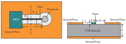
Fig. 9 Top and Cross-Sectional Views of Trace Line in PCB
The capacitance per unit length of the trace is an important concept to emphasize the need for short traces. Increasing the distance of the trace increases the parasitic capacitance associated with the trace. Increasing the trace length can also increase susceptibility to noise. Therefore, the trace routing between the microcontroller and the electrode should be kept as short as possible. This is not always possible, so it is important to understand the increase in parasitic capacitance associated with the trace routing.
Capacitance per Unit Length
The capacitance per unit length should be kept as small as possible to minimize the parasitic capacitance (C_trace) and ultimately maximize sensitivity. As previously mentioned, the dominant capacitance in C_trace is the parallel plate capacitance between the trace and the surrounding ground pour. The ability to reduce this capacitance is a direct function of the PCB manufacturing capabilities. Tighter tolerances and smaller minimum dimensions (trace width and separation) allow for thinner traces and larger separation, which result in lower capacitance per unit length. These manufacturing capabilities typically come at a higher cost.
The table below shows how the capacitance per unit length changes with the variation of different dimensions. These values are taken from Reference Section in the Coplanar Waveguide Analysis/Synthesis Calculators.
W (mm) |
S (mm) |
T (mm) |
H (mm) |
Er |
C (pF/cm) |
|---|---|---|---|---|---|
0.152 |
0.152 |
0.036 |
1.6 |
4.6 |
0.633 |
0.152 |
0.254 |
0.036 |
1.6 |
4.6 |
0.555 |
0.152 |
0.381 |
0.036 |
1.6 |
4.6 |
0.496 |
0.203 |
0.152 |
0.036 |
1.6 |
4.6 |
0.692 |
0.203 |
0.254 |
0.036 |
1.6 |
4.6 |
0.602 |
0.203 |
0.381 |
0.036 |
1.6 |
4.6 |
0.543 |
0.254 |
0.152 |
0.036 |
1.6 |
4.6 |
0.740 |
0.254 |
0.254 |
0.036 |
1.6 |
4.6 |
0.641 |
0.254 |
0.381 |
0.036 |
1.6 |
4.6 |
0.578 |
0.254 |
0.152 |
0.036 |
2.54 |
4.6 |
0.736 |
0.254 |
0.254 |
0.036 |
2.54 |
4.6 |
0.637 |
0.254 |
0.381 |
0.036 |
2.54 |
4.6 |
0.566 |
Table: Calculating Results of Capacitance per Unit Length
The table above shows that increasing the space, S, between the trace line and the ground is an effective way to reduce the parasitic capacitance. However, increasing the separation can have negative effects that need to be understood. One effect is simply increased board space. Increasing the dimensions can lead to larger PCBs and higher cost. Another effect is related to noise. The larger separation makes traces more sensitive to touch events (touching the trace instead of the electrode) and more susceptible to radiated emissions.
In practice, the designer should choose a balanced S value, and a value of 1/8 of the overlay thickness is typically acceptable. Additionally, a hatched ground is commonly used instead of solid fill near the trace lines to reduce the area and consequently the parasitic capacitance.
The table above also shows that as H gets smaller, the parasitic capacitance increases, which results in a decrease in sensitivity. In most applications, a two-layer PCB is used, and a standard FR4 PCB with the thickness of 1 mm to 1.6 mm is recommended. If a multilayer board is used, it is recommended to keep the H as large as possible. With complex multilayer boards (more than six layers), it is important to recognize that the absence of copper in the internal layers can cause issues and the height, H, between the top layer and the bottom may be smaller than predicted.
The figure below shows an example of a four-layer PCB, which may be desired in applications with limited board space. To reduce parasitic capacitance, the ground pour is usually placed on the lowest layer underneath the trace to provide the largest H. If it is difficult to achieve the maximum height, then a narrower W, a larger S, or even a hatched ground fill are alternatives to reducing the parasitic capacitance.
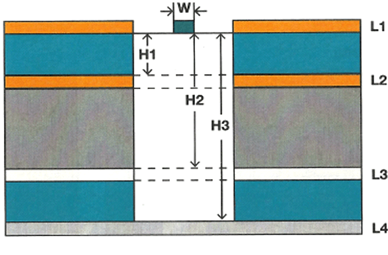
Fig. 10 Trace Without Copper Pouring Underneath in Multilayer PCB
To determine the maximum trace length from the capacitance per unit length, some additional information is needed. The following example is used to calculate the maximum distance for a trace with a capacitance per unit length of 0.58 pF/cm. The capacitance introduced by a touch, C_touch, is assumed to be approximately 1 pF. To make sure that the capacitance induced by a finger is large relative to the parasitic capacitance, the total parasitic capacitance (C_parasitics, C_trace, and C_electrode) should be in the range of 10 pF to 20 pF (the change is at least a 5% change). Assuming that the C_electrode is approximately 3 pF, the C_parasitics is 5 pF, and the capacitance per unit length is 0.58 pF/cm, so the trace line length L should be no longer than 210 mm. If the electrode is larger (for a proximity application), the capacitance itself is larger (assume approximately 8 pF for this example), so the maximum trace line length L is reduced to 120 mm.
Generally speaking, the trace width W should be as thin as the PCB technology allows, because a short and narrow trace line is preferred. The trace thickness T and the relative permittivity of the material Er also have significant influence on capacitance per unit length, but they are determined by PCB manufacture process and are usually difficult to change.
Connectors
Some designs require the electrode to be off-board, and consequently a connector is used to transition the trace from the PCB to a cable or to another PCB. Connectors are generally not desired because like any component there is an associated parasitic capacitance with connector PCB footprint and structure.
In terms of parasitic capacitance and sensitivity, the connector is treated as a parasitic capacitance reducing the sensitivity of the solution. Because the connector is treated as a lumped capacitance, the placement is irrelevant to the sensitivity. However, the placement is important with respect to noise.
The figure below shows that if the aggressor (noise source, N1) is located on the PCB, then the preferred placement of the connector is near the MSP430 microcontroller. The parasitic capacitance associated with the connector shunts high-frequency noise (Z 1/jwC) and increases the noise immunity of the circuit. Conversely, if the aggressor is located off-board (noise source, N2), then the connector should be placed farther from the microcontroller and closer to the electrode. This arrangement minimizes the off-board trace and cable length (which acts like an antenna). When multiple aggressors exist as is shown in the figure below, it is recommended to reduce the effect of the radiators that most closely match the operating frequency of the touch detection circuit.
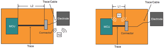
Fig. 11 Top View of Connector and Noise Source
When deciding the position of the connector, the designer must balance the length of the trace and the cable while considering parameters like the background noise.
Routing Material
The routing is typically done with copper, but other materials like silver and ITO can be used. Silver is similar to copper and similar performance can be expected (if the thickness of the materials are also equivalent). ITO is very different from copper, and the difference in resistivity degrades the sensitivity of the solution. Lowering the impedance of the trace (by increasing the width) should be a high priority in the design, even though this comes at the cost of increased parasitic capacitance and reduced noise immunity. Ultimately, the use of materials like ITO requires more processing by the MSP430 microcontroller to adjust to lower sensitivity and increased noise.
Electrode Material
As discussed in the Routing section, conductivity becomes an issue in more resistive materials like ITO. Although the transparency of ITO is very good, the resistivity is high when compared to materials like silver and copper. Typically the physical dimensions prohibit increasing the area of the ITO electrodes, and therefore any degradation in sensitivity must be compensated for in the firmware. This typically results in slightly longer measurement times and consequently increased power consumption.
Electrode Design
The electrode design must accomplish two goals. First, the design must provide sufficient signal (change in capacitance with interaction). The design must project the e-field up and out so that the appropriate level of sensitivity is achieved at the desired distance. Understanding the stackup, thickness and dielectric, the electrode can be sized and shaped to provide the maximum signal. Second, the electrode design needs to have a minimal parasitic capacitance.
In the following sections the shape and area of the electrode are discussed with the intent of maximizing the signal for different implementations (buttons, sliders, and wheels). The basis for controlling the parasitic capacitance is common to different sensor implementations and is discussed here.
The figure below shows an example PCB cross-section and the important parameters that influence the parasitic capacitance. The height, width, and separation have a direct effect on the parasitic capacitance of the electrode, C_electrode. The fundamental parameter area is not shown in the figure below because this has a direct effect on both the touch capacitance (C_touch) and the parasitic capacitance (C_electrode). This section describes how changes to the height and separation can minimize the parasitic capacitance. The following sections describe how changes to the area can maximize C_touch.
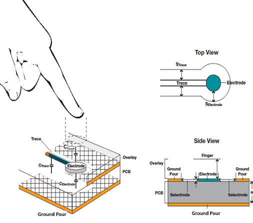
Fig. 12 Capacitance of the Electrode
The separation (S_electrode) is directly related to the height of the overlay as described in the Mechanical section. The height is a function of the PCB and is not a parameter that can be easily controlled. The separation is typically the parameter with the most flexibility.
Area(mm2) |
Height(mm) |
Description |
Separation(mm) |
Capacitance(pF) |
|---|---|---|---|---|
10x10, FR-4 (Er = 4.4) |
1.572 |
2 Layer PCB, L2 |
0.508 |
3.3 |
10x10, FR-4 (Er = 4.4) |
1.572 |
2 Layer PCB, L2 |
1.02 |
3.2 |
10x10, FR-4 (Er = 4.4) |
1.572 |
2 Layer PCB, L2 |
1.52 |
3.1 |
10x10, FR-4 (Er = 4.4) |
1.30 |
4 Layer PCB, L2 |
0.508 |
3.8 |
10x10, FR-4 (Er = 4.4) |
1.57 |
4 Layer PCB, L3 |
0.508 |
3.3 |
Table: Baseline Electrode Capacitance
The table above shows that increasing the height (the distance between the electrode and the reference plane) decreases the capacitance. By decreasing the parasitic capacitance, the relative change in capacitance caused by a touch event is increased. For example, if the change in capacitance associated with a touch is 0.5 pF, the relative change is greater when the base capacitance is 11 pF instead of 12 pF, (4.5% instead of 4.2%).
Spacing Between Electrodes
By default, the CapTIvate™ Software Library drives non-actively scanned electrodes to ground allowing neighboring electrodes to be treated as an extension of the ground pour. Therefore, the spacing between the electrodes follows the same rules for spacing from ground. The goal is provide enough spacing so that the e-field propagates up and through the overlay material. A minimum spacing of one-half the overlay thickness has been found to provide sufficient signal (sensitivity). For example, a 3mm overlay material would suggest a minimum spacing of 1.5mm or greater between electrodes or between electrodes and ground. Note, for overlay thickness less than 2mm, maintain the spacing to no less than 1mm.
Shapes
The capacitance of the electrode is a function of area, but the shape is important to consider, because the shape can influence the area. An important detail of designing the electrode shape is not to design shapes that have low surface area. The area of each electrode must provide the maximum C_touch, which in turn produces the most signal (the change in capacitance) when a touch event occurs.
Crosstalk
In the Connectors section above, the aggressor is assumed to be a point source of noise. In this section, the aggressors are different signals that are routed in close proximity to the capacitive touch sensor trace. These aggressors can be another capacitance sensor trace or non-capacitance sensor lines. Examples of non-capacitance sensor lines include digital signals, analog signals, and high-current signals used to drive LEDs.
Adjacent Capacitive Touch Signals
Capacitive sensor traces influence neighboring capacitive touch sensor traces. The space between capacitance sensor trace lines, Scs, should be kept as a safe distance (see figure below).
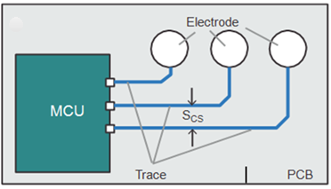
Fig. 13 Trace Spacing
Digital Signals
Digital signals are typically PWM signals or communications like I2C or SPI. Unlike the capacitive traces, these signals can act as aggressors and can be active during a capacitance measurement. It is recommended to keep these types of signals at least 4 mm away from the capacitive touch trace. If the digital signal and the capacitive touch trace must cross, then it is recommended to keep the crossing at a 90 degree angle.
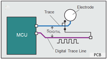
Fig. 14 Digital Traces
LEDs/LED Backlighting
Signals used to drive LEDs (unless the LEDs require high-strength drivers) are similar to other digital signals. As with digital signals, a distance of at least 4 mm is strongly recommended for S_LED as shown in the figure below.
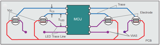
Fig. 15 LED Traces
As a general rule, LEDs should be driven and the use of high-impedance states should not be used to control the LED. The use of a high impedance to prevent an LED from conducting can result in a significant difference between the on-state and off-state capacitances. This change in capacitance may be detected by the touch solution and treated as a change in the system capacitance, or even worse as a false detection. If the use of high-impedance control of the LED is unavoidable, a discrete capacitor (typically 1 nF is acceptable) in parallel with the LED is recommended.
Avoid tri-stating the LED as the LED capacitance will change when turned on and off
If LED must be tri-stated, add small bypass capacitor to control change in LED capacitance
Capacitor does not have to be physically near LED, just in the circuit
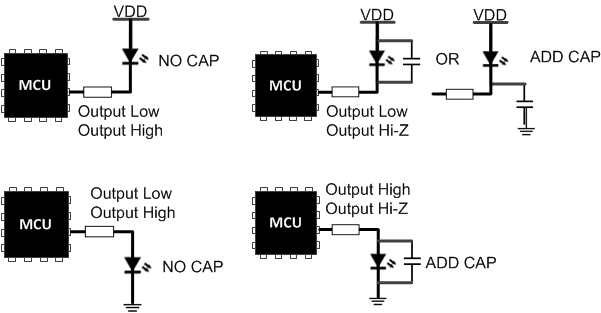
Fig. 16 Recommended methods to drive LEDs
LED BackLighting can be done easily using a back lighting LED on the opposite side of the PCB
Keep hole as small as possible to eliminate possible dead spots in sensor
LEDs may require bypass capacitor (see above)
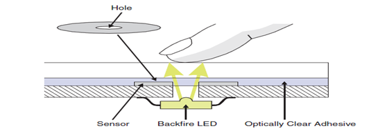
Fig. 17 Backlighting LEDs
As an example of an LED backlighting technique, the following wheel design has an LED mounted on the backside of the PCB and illuminates through a small hole. In parallel to the LED, a small 1nF capacitor is used to reject changes in capacitance when the LED is switched between ground and high-Z. Also note the hatched ground on both the top and bottom layers to help with noise immunity.
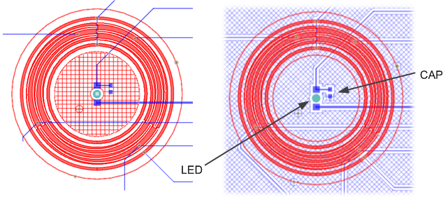
Fig. 18 LED BackLight Example
Ground Planes
Why you want to have a Ground pours around the sensors?
Ground planes have a purpose by helping with noise immunity and cross-talk between neighboring sensors. Although generally recommended, the amount of fill (solid vs a hatched) depends on the system environment.
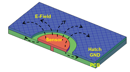
Fig. 19 Ground Pours
What are the trades-off?
Parasitic capacitance
The ground pours add the parasitic capacitance into the base capacitance as the separation from the ground decreases and the area of the ground pour increases. As shown in the illustrations, adding a hatched or solid ground pour will increases the total sensor capacitance, making it less sensitive to the small change in capacitance caused by a touch condition. Fortunately the CapTIvate peripheral has the ability to subtract off these parasitic effects, restoring a sensor’s sensitivity.
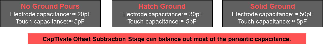
Fig. 20 Ground Pours Parasitic Capacitance Trade-off
Electric field
These same ground pours can also have a negative effect by pulling the sensor’s electric field towards the ground pour, creating a potentially large parasitic capacitance. This parasitic capacitance degrades the overall strength of a touch signal, making the sensor less sensitive to a touch condition. As shown in the illustration, more of the sensor’s electric field lines are attracted to the ground pour rather than extending outward from the sensor. This effectively reduces the strength or range of a sensor to a touch condition. However, the system cannot re-gain the electric field strength.
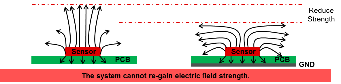
Fig. 21 Ground Pours Electric Field Trade-off
Planes and pours near the electrode and trace must be connected to a potential and cannot be left floating or in a high impedance state. Such structures serve as a mechanism for noise coupling and are strongly discouraged.
Separation
Ground planes, both coplanar and on neighboring PCB layers, reduce noise. This is the same principle discussed in the Routing section. The ground or guard structures are placed as close as possible to reduce noise but also kept far enough away to minimize parasitic capacitance. This separation is a function of the thickness of the materials (overlay, adhesive, etc.) on top of the trace. As mentioned in the Routing section, a good rule is one-eighth the thickness for separation between traces and ground. The separation between electrodes and ground should be at least one-half the thickness.
Fig. 22 Ground Separation
As shown in the figure above, the separation between the electrode and the coplanar ground pour should be at least one half the thickness of the overlay material. Any unused electrode should be held at a logic low level (Vss potential) and not allowed to float. In this way the spacing between electrodes is the same as the ground and electrode distance.
Pour
The use of a hatched pour instead of a solid ground pour is a good design practice. This reduces the area and consequently the parasitic capacitance associated with both C_trace and C_electrode. Typically, a 25% fill hatch is sufficient, but this percentage can be increased or decreased to improve noise immunity or sensitivity, respectively.
Fig. 23 Example Hatched Ground Fill
Using Poly Cut Out to control Ground Pour around Sensors
When designing a button, slider or wheel of any size or shape, a flexible method to control the distance between any sensor and the ground pour is to provide a poly cut-out region around the sensor as shown below.
Fig. 24 Define Poly Cut Out Region
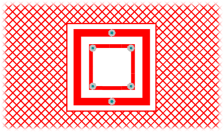
Fig. 25 Ground Pour Spacing Controlled
Mutual Capacitance Traces
Routing mutual capacitive traces has special considerations compared to self capacitive traces. Specifically, the TX and RX signals on the same layer should be close only in those areas where coupling through a finger touch is expected by design, such as the case with button, slider or wheel elements (electrodes). Anywhere else that TX and RX traces on the same layer are routed close can be susceptible to a “ghost” touch should a finger touch in that area.
Traces
Avoid routing TX lines near RX lines when possible
Within a finger spacing, they will create a button
If unable to avoid on same layer, put ground trace in between (adds parasitic capacitance)
If TX needs to cross RX, make crossing perpendicular (minimize surface area intersection)
Avoid running TX on one layer of PCB parallel to RX on other layer of PCB
Route TX lines next to other TX lines
Route RX lines next to other RX lines
Keep nearby ground away from TX and RX traces by 1/2 panel thickness (reduces parasitic capacitance)
The diagram below shows an 8-button keypad using (2) TX and (4) RX traces. In this layout the TX and RX traces are on the same layer. The TX traces are routed close to each other as are the RX traces. The TX traces are routed away from the RX traces. In this example there is one RX that must be routed near a TX trace. A ground trace/fill is used to separate the RX and TX traces.
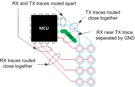
Fig. 26 Routing mutual capacitance sensors
Electrodes
For noise suppression, use 25% hatched ground on:
Bottom layer of PCB and/or
On top layer of PCB keeping ground 1/2 panel thickness away from electrode
CapTIvate Pin Selection
It is important to consider the electrode-to-pin mapping early in the design process, as the pin selection can have significant impact on performance. The pin mapping primarily effects the following parameters:
Measurement time and power consumption, in designs with more than one electrode
Parasitic capacitance, in designs using mutual capacitance
Signal crosstalk, in designs where digital port pins are switching near the CapTIvate pins.
CapTIvate Pin Nomenclature
CapTIvate pins are named CAPx.y on a device datasheet and in the CapTIvate Design Center. In this scheme, ‘x’ refers to the CapTIvate block the pin is connected to, and ‘y’ refers to the ID of the pin on that CapTIvate block. A CapTIvate block is a capacitance-to-digital conversion engine, and many CapTIvate devices have multiple blocks to enable parallel measurement of multiple sensors, reducing measurement times. For example, let’s consider a design with two buttons. On an MSP430FR2522 MCU, we could connect those two buttons to the same block or to two different blocks. If we connected both buttons to CAP0.x (say, CAP0.0 and CAP0.1), then we would have to measure them sequentially (one after the other) since they both share the same measurement engine. However, if we would have connected them to CAP0.0 and CAP1.0, we would have been able to measure them at the same time- resulting in half the measurement time. This reduction in measurement time gives the flexibility of being able to reduce power consumption or increase the scan rate to improve the responsiveness of the sensors.
Electrode to Pin Assignment Procedure
To obtain an optimum routing, it is recommended to either assign pins automatically (using the CapTIvate Design Center Auto-Assign feature), or manually, using the procedure outlined below.
If the design has more than one electrode (more than one button), and the device selected has more than one CapTIvate block, it is best to assign RX’s to separate CapTIvate blocks. This allows for parallel scanning, which reduces measurement time and power consumption. To determine if the device being used has more than one block, check the device family chapter.
If the design has mutual capacitance sensors, select the TX pins to be as far away as possible from the RX pins. This reduces parasitic mutual capacitance between the RX’s and TX’s, and improves sensitivity. As a general rule, it is still best to spread the RX’s out across different blocks before considering this step.
If you plan to have digital IO’s on the MCU that are switching in a frequency range similar to the electrode acquisition frequency, it is best to isolate those signals as much as possible from any RX pins to reduce noise resulting from trace crosstalk. The frequency range of concern is generally 500kHz to 4 MHz. Common offenders in this area are SPI signals and PWM signals routed near sensor RX traces.
Buttons
Self Capacitive Buttons
A self capacitive button sensor is a single electrode. Self capacitive buttons are simple to layout and each button is assigned to only one pin on the MCU. Self capacitive buttons will provide greater sensitivity as compared to a mutual capacitive button, but are more influenced by parasitic capacitances to ground.
Parameter |
Guidance |
|---|---|
Radiation Pattern |
Between Electrode and Ground |
Size |
Equivalent to interaction |
Shape |
Various: typically round or square |
Spacing |
0.5 x Overlay minimum thickness |
Fig. 27 Example Self Capacitive Button Designs
Self Capacitive Button Shapes
The electrode shape is typically rectangular or round with common sizes of 10mm and 12mm. Ultimately, the size will depend on the required touch area. A good design practice is to keep the size of the button as small as possible, which minimizes the capacitance and will help with the following:
Reduce susceptibility to noise
Improve sensitivity
Lower power operation due to smaller capacitance and reduced electrode scan time
In the diagram below, an example silkscreen button outline pattern is shown.
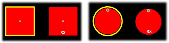
Fig. 28 Example Self Capacitive Button Designs
The goal of the button area is to provide sufficient signal when the user touches the overlay above the button electrode. Typically a nonconductive decal or ink is used to identify the touch area above the electrode. The relationship between the decal and the electrode can be varied so that contact with the outer edge of the decal registers a touch. Conversely, the electrode could be small to ensure that the button is activated only when the center of the decal is touched. The two figures below show how the effective touch area is a function of the electrode size and the size of the finger.
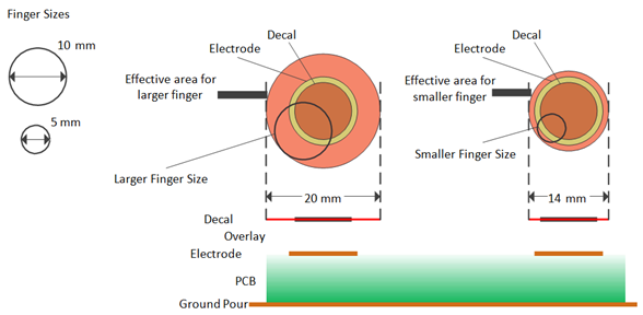
Fig. 29 Effective Area Example for Electrodes Larger Than Decal
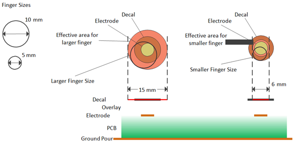
Fig. 30 Effective Area Example for Electrode Smaller Than Decal
One common mistake is to make the electrode the same shape as the icons printed (in nonconductive ink) on the overlay. As shown in the figure below, this can lead to electrodes with odd shapes that create discontinuities and reduce surface area.
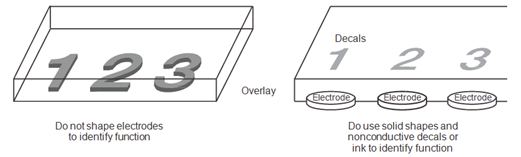
Fig. 31 Button Shape Examples, Dos and Don’ts
As the distance of the overlay increases, the effective area decreases. Therefore, it is important to keep the button electrode diameter at least three times the overlay thickness.
Mutual Capacitive Buttons
A mutual or “projected” capacitive button sensor requires two electrodes, one as a TX and the other for RX. It is possible to pack the electrodes closer together with a low risk of cross talk between neighboring electrodes. With mutual capacitive electrodes, multi-touch is also possible by multiplexing the channels. Multiplexing creates up to 64 electrode pairs or “buttons” that can be scanned using only 16 CapTIvate™ I/O pins.
Parameter |
Guidance |
|---|---|
Radiation Pattern |
Between TX and RX and ground |
Size |
Equivalent to interaction |
Shape |
Various: recommend square or shape with corners |
RX-to-TX Spacing |
0.5mm typical |
RX Thickness |
0.5mm typical |
TX Thickness |
1mm typical |
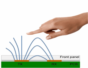
Fig. 32 Example Mutual Capacitive Button Designs
Mutual Capacitive Button Shapes
The electrode shape is typically rectangular with common sizes being 10mm and smaller. Ultimately, the size will depend on the required touch area. In the diagram below, the TX and RX electrodes are identified and a suggested silkscreen button outline pattern is shown. The position of the vias on the TX and RX electrodes provide flexible signal connection points when routing traces.
Simple Square Electrode
Easiest to layout
Highest sensitivity
TX on outside, RX on inside
For single layer designs, can open TX on one side and feed RX trace through (preferably not in a corner)
Better sensitivity if traces on two layers
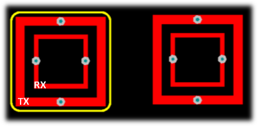
Fig. 33 Example 10mm Mutual Capacitive Button Design)
A good design practice is to keep the size of the button as small as possible, which minimizes the capacitance and will help with the following:
Reduce susceptibility to noise
Improve sensitivity
Lower power operation due to smaller capacitance and reduced electrode scan time
The dimensions shown on a 10mm x 10mm example button are suitable for overlay thickness up to 2mm.
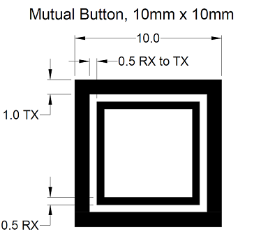
Fig. 34 10mm Mutual Capacitive Button Dimensions
Mutual Capacitive TX / RX Electrode Spacing Considerations
The RX-TX spacing is an important design parameter that affects sensitivity, measurement time, and reliability. This is because the RX-TX spacing is a key contributor to the size of the base mutual capacitance that is built in to the PCB. The closer the RX and TX are to each other, the higher the base mutual capacitance. The farther apart they are, the lower the base mutual capacitance. Having a higher base mutual capacitance improves measurement accuracy and repeatability by providing a larger RX voltage swing during measurement. However, the downside of this is that the sensitivity is reduced (because of the higher mutual capacitance, and the lower E-field propagation). TI’s recommended value for most applications is an RX-TX spacing of 0.5mm.
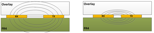
Fig. 35 Example Mutual Capacitive Button Designs
As mentioned earlier, mutual capacitive electrodes can be multiplexed with other mutual capacitive electrodes. This means that more than one button can share a common signal. In the 8-button example below, the design of the button and placement of vias allow for easy routing to the neighboring buttons. Depending on the orientation of the routing signals, the buttons could be rotated if needed. Taking advantage of CapTIvate™ Technology hardware feature allowing up to four channels to be scanned in parallel, the top four RX channels are measured while TX_0 is driven. The sequence is then repeated for the bottom row. Scanning four channels in parallel reduces the device’s overall power by reducing the scan time by 4x and it should become apparent that the eight buttons were measured with only six CapTIvate™ I/O pins.
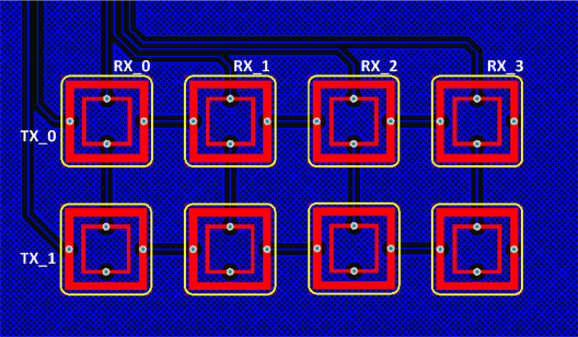
Fig. 36 8-Button Multiplexed Mutual Capacitive Example Design
Button Performance as a Function of Overlay Thickness and Electrode Size
A system’s performance can depend on a variety of parameters, but those parameters that have the greatest impact are the overlay material, overlay thickness and type of electrode and electrode size. Pictured below is a test PCB electrode board containing self and mutual electrodes with different dimensions that was used to collect the data summarized in the following graphs. The graphs show the expected performance differences (signal level) for each of the different combinations.
Test Setup
The test PCB is a 2 layer design with ~25% hatched GND (8mil trace width, 56mil spacing) on Top and Bottom layers. The square button dimensions are 15, 12, 10, 8, 6, and 4mm. The circular button diameters are 15, 12, 10 and 8mm. The first two columns are self capacitive buttons while the other two columns are mutual capacitive buttons with RX to TX spacing is equal to 0.5mm in the third column and 1.0mm in the fourth column.
The following items were used for testing:
Material and Thickness: Glass: (4, 6) mm, Plexi Glass: (4, 6) mm
Filler material: double sided tape ~0mm
Test finger: grounded metal ring 12mm diameter
Fig. 37 Test PCB
Fig. 38 Test Setup
To compare results, the “Signal Strength” is expressed as percent (%) change in capacitance due to a touch, as measured using the CapTIvate Design Center SNR tool. The Conversion Count and Conversion Gain parameters are adjusted for optimal performance to cover the worst case scenarios of thick overlays and small electrodes.
For all tests the Conversion Gain is set to 100. The Conversion Counts for both Self and Mutual Electrodes are shown:
500 for 4mm glass overlay
1000 for 6mm glass overlay
1000-1200 for 4 and 6mm plexi-glass
The parameters are adjusted to allow a valid touch detection for each case. Instead of a real finger, a grounded Ø 12mm metal ring is used and placed directly on the overlay.
The overlays are bonded to the PCB a double sided tape, such as a 3M 467MP pressure sensitive adhesive. Depending on Gen1 or Gen2 devices, different recommended limits apply. Refer to the device family chapter for details. Additional information on the SNR tool and recommended limits can be found at Sensitivity, SNR, and Design Margin in Capacitive Touch Applications. The recommended limits are super-imposed on the graphs to help users identify the areas and conditions under which their system can operate reliable. These results provide a first assessment of the expected performance for different HW configurations during the concept phase.
Performance Self Capacitance
The performance results for Self capacitance configurations can be seen in the graph below. The minimum recommended limits for Gen1 (Red limit) and Gen2 (Black limit) are given in the graph. Values above the Red line indicate a reliable operation of the system for Gen1 devices. Values above the Black line indicate a reliable operation for Gen2 devices.
For example, using a 4mm plexi glass overlay, the minimum button size for a Gen1 device is 100 mm2 (a 10x10 mm button). For the Gen2 device, the minimum button size is 36 mm2 (a 6x6 mm button).The minimum recommended threshold is based on the SNR and design margin analysis, please set the threshold accordingly based on your system design.
Fig. 39 Self Capacitive Plot
Performance Mutual Capacitance
The performance results for Mutual capacitance configurations can be seen in the graph below. The minimum recommended limits for Gen1 (Red limit) and Gen2 (Black limit) are given in the graph. Values above the Red line indicate a reliable operation of the system for Gen1 devices. Values above the Black line indicate a reliable operation for Gen2 devices.
For example, using a 4mm plexi glass overlay, a 10x10 mm button (100 mm2) button size will provide more than enough signal strength for both Gen1 and Gen2 devices. The flatter behavior of the curve is specific to Mutual capacitance and caused by the fact that the field is generated between the TX and RX electrode which have a fixed distance. This leads to a flat performance behavior across the different electrode sizes. The sensitivity for mutual mode is mainly depends on the overlay material, overlay thickness and the space between TX and RX.The minimum recommended threshold is based on the SNR and design margin analysis, please set the threshold accordingly based on your system design.
Fig. 40 Mutual Capacitive Plot
In summary, the two graphs above can help a user determine an appropriate size button and device for a given overlay thickness.
Sliders and Wheels
Sliders and wheels are multi-element sensors that create a linear HMI user input for such things as audio volume, LED color blending and light brightness controls. CapTIvate Software Library supports sensors ranging from 3 to 12 elements, however, more common are sliders and wheels with only three or four elements. While it is certainly possible to use more elements, the layout becomes increasingly difficult to route, requiring more CAPTIVATE IO pins and generally does not improve the sensor’s performance. Shown here are examples of self and mutual capacitive 3-element wheel and 4-element slider designs.
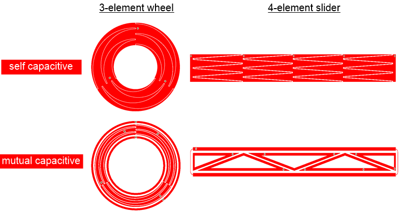
Fig. 41 Example - Wheel and Sliders
Self or Mutual Capacitive?
*Self*
Simple to design and route
One CAP IO pin per electrode
*Mutual*
RX elements can be multiplexed with other sensors in the system requiring fewer CAP IO pins
Creates a local e-field between RX and TX electrodes reducing cross-talk with adjacent sensors in close proximity
Better moisture rejection
How Many Electrodes?
As mentioned above, most applications can implement a 3 or 4 element slider or wheel with excellent performance. One feature of CapTIvate on devices with 4 measurement blocks, such as the MSP430FR2633 and MSP430FR2676, is the ability to scan 4 elements (one element per block) in parallel in a single measurement cycle. Measuring all sensor elements in one cycle has the following benefits:
Most power efficient
Least measurement time
Best linearity
Shown here is an example of a 4-element self capacitive slider and wheel with the recommended connections selected by the CapTIvate Design Center’s “Auto Assign” button. Notice how the design center chose a configuration with each sensor element connected to only one pin from each CapTIvate measurement block. In addition, the selected pin is the first pin from each block. By default, the first pin of each block is assigned to measurement cycle 0 and is represented in the CapTIvate Design Center Sensor properties View by showing these pins (light blue) in parallel group “B0”. It is possible to manually assign pin connections and measurement cycles as described in the CapTIvate Design Center User’s Guide and discussed later in this section.
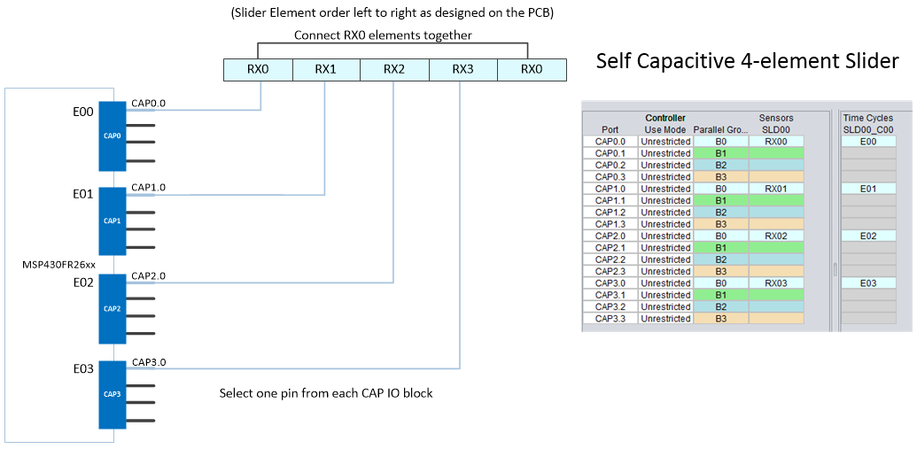
Fig. 42 Example - 4 Element Slider
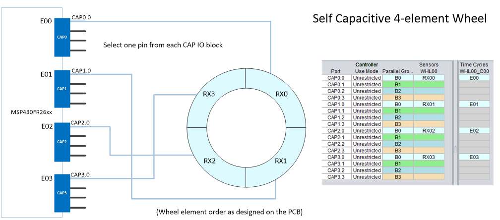
Fig. 43 Example - 4 Element Wheel
Slider and wheel sensors with more than 4-elements are supported but may not provide any additional benefits compared to the performance of a 3 or 4-element sensor. For example, sensors with more than 4-elements require additional measurement cycles, which increases the overall measurement time and increases power consumption. Shown here is an example of a 5-element self capacitive wheel. Notice the first 4-elements are measured in cycle 0 (light blue) and the 5th element is measured cycle 1 (green).
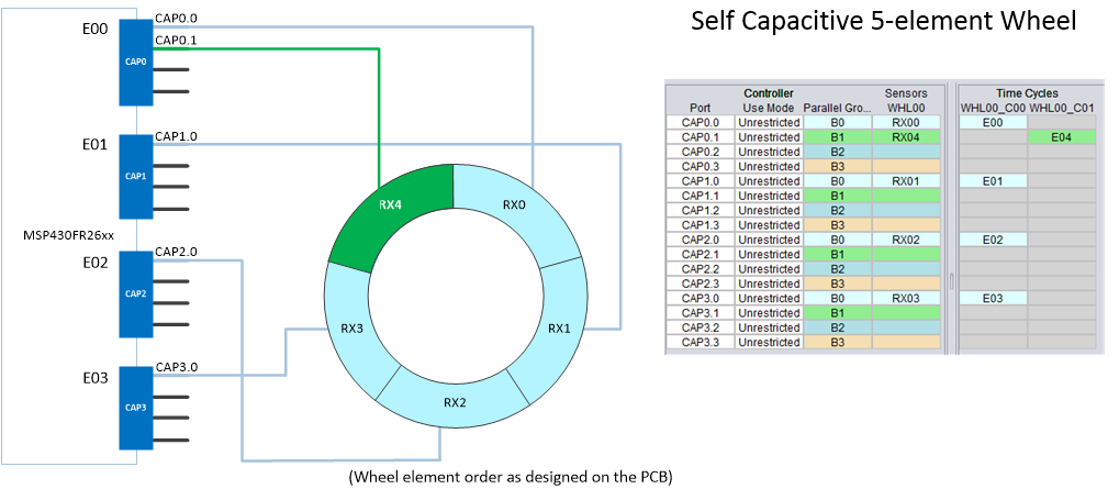
Fig. 44 Example - 5 Element Wheel
There is an additional down-side to using more than 4 elements; measuring the elements in two time cycles can influence the sensor’s linearity. Contrary to the belief that sensors with more elements will provide a better linear response is not true in this case. In this wheel example, during measurement cycle 0 (light blue) the first 4-elements are measured while the 5th element is held at ground potential. During measurement cycle 1 (green) the 5th element is measured while all of the other elements are held at ground potential. Elements at grounded potential can affect the sensitivity of their neighboring active elements resulting in a less optimal linear response.
Fig. 45 Example - 4-Block Less than Optimal Linearity
This same linearity issue is also true for devices with fewer than 4 blocks, such as the MSP430FR2522 with only 2 measurement blocks. Multiple measurement cycles are required, affecting the performance as described above. This is one reason why devices with fewer than 4 blocks are generally not recommended for slider and wheel applications. For best performance, consider implementing a 3 or 4-element sensor using a device with 4 measurement blocks.
Fig. 46 Example - 2-Block Less than Optimal Linearity
One exception to the recommendation for using no more than 4 elements might be if the wheel or slider sensor is very large, resulting in elements with a large surface area. As an element’s surface area increases, so does it’s base capacitance, reducing its sensitivity and increasing its susceptibility to conducted noise interference. Using additional elements can help by reducing an element’s baseline capacitance. However, be mindful of the trade-off as described above.
Connecting the Sensor to the MCU
Deciding how to connect the sensor to the MCU is traditionally driven by selecting the pins that create the most efficient PCB layout. However, in the case of CapTIvate, randomly selecting CAP IO pins is not recommended and will most likely not provide optimal performance and in many cases not work. To avoid this problem, it is strongly recommended to use the CapTIvate Design Center’s Auto Assign feature to determine the optimal connections between the sensor and the MCU. There is a specific order, as shown in the following illustrations, which the sensor’s electrodes must be connected to the CapTIvate measurement blocks for the software algorithm to properly process the measurements. If this order is not followed, the slider or wheel sensor will not work properly.
The general rule to connect a multi-electrode sensor is:
Connect first electrode to block 0
Connect second electrode to block 1
Connect third electrode to block 2
Connect fourth electrode to block 3
Selecting the same pin on each block ensures the those pins will be measured in parallel during the same measurement cycle (options to select alternate pins described later).
Fig. 47 Example - Sensor Element Processing
For sensor’s with more than 4 electrodes, repeat the sequence for the fourth, fifth, sixth, … electrodes as shown here in the 8 element sensor example.
Fig. 48 Example - Multi-Cycle Sensor Element Processing
Custom Pin Assignment
As mentioned above, not all sensor layout designs can follow the general connection rule described above due to PCB routing restrictions. In these cases there is some flexibility to allow swapping pin assignments after the default sensor configuration has been created by the CapTIvate Design Center. In the example illustrated below, a PCB designer has determined that due to the placement of the MSP430FR2633 on the PCB it is more efficient to route traces from E01 to RX2 rather than to RX1. This breaks the general rule for pin assignments, however, in this case it is ok to connect E01 to RX2 and connect E02 to RX1 because they are in the same measurement cycle. The sensor configuration in the CapTIvate Design Center must updated to reflect this change, as shown below, else the sensor configuration in the “CAPT_UserConfig.c” will be wrong and the slider will not function properly. It is simple to make this change using a feature that allows any pin to be swapped with another pin, as long as both are in the “same” measurement cycle. Remember, this only works when the elements are in the same measurement cycle. Sensors with more than one measurement cycle cannot swap pins between “different” measurement cycles. Refer to the CapTIvate Design Center User’s Guide for more information about modifying pin connections.
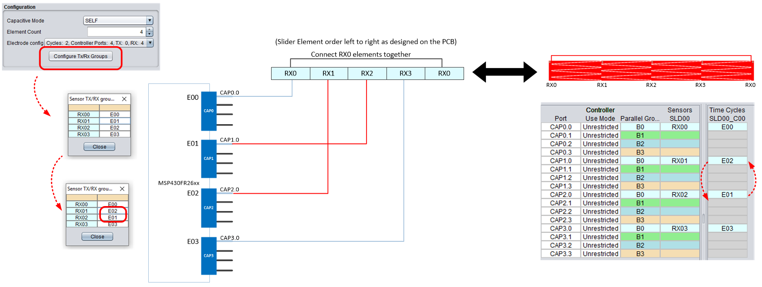
Fig. 49 Example - Swapping Sensor Electrode Order
The majority of designs will require some customization from an initial sensor configuration or the designer may simply prefer to choose all of the pin connections manually based on the routing limitations on their PCB. This example below shows the pin connections the designer chose. The designer followed the pin assignment ordering rule and assigned the sensor’s first electrode to block CAP0, second electrode to block CAP1, third electrode to block CAP2 and finally the last electrode to block CAP3. However, instead of choosing the first pin from each block the designer chose different pins because it was more efficient to route the PCB traces between the sensor and MCU. This will work but as you can see this forces the pins into four different measurement cycles which will take 4 times longer and cause an increase in power. Fortunately there is a feature that can enable the measurement cycles (Parallel Groups) to be swapped around and put these four pins into the same measurement cycle. Notice that all of the pins are now in the same time cycle 0, parallel group B1. Refer to the CapTIvate Design Center User’s Guide for more information about modifying pin connections.
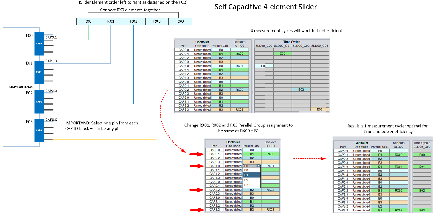
Fig. 50 Example - Manual Pin Assignments
Sensor Resolution
CapTIvate Technology’s increased sensitivity combined with the CapTIvate Software Library provide exceptional linearity and accuracy for slider and wheel resolutions well beyond 10-bit of resolution. A slider or wheel will report position from 0 to the assigned (resolution - 1). As an example, if a slider or wheel has a resolution of 1000, the sensor will report 1000 positions, from 0 to 999.
PCB Sensor Designs
For both sliders and wheels, the area of the electrode is not as critical as the percentage of coverage across multiple electrodes. As shown in the examples below, inter-digitated slider and wheel designs provide the most efficient and optimal coupling, but can be complicated to create. Simpler designs are possible, but require experimentation. In general, self capacitive slider and wheel sensors are more common that a mutual capacitive slider and wheel sensors.
Self Capacitive Sensor Shapes
To help simplify and automate the process of creating a self capacitive slider or wheel layout, See Application Note SLAA891 - Automating Capacitive Touch Sensor Design using OpenSCAD Scripts. This document describes how to create scalable self-capacitive slider or wheel sensors in seconds with OpenSCAD, a free Solid 3D CAD modeling tool and custom scripts created by Texas Instruments. There is no need to re-draw anything. Simply modify a few script parameters and a slider or wheel design can be re-scaled to any size, any number of electrodes (elements), with any spacing, and more. Designing a slider or wheel with great performance is easy.
Designing a Self Capacitive Slider
A note about connections to self and mutual capacitive sliders. Self and mutual sliders require their RX0 electrode on both ends of the slider be electrically connected on the PCB layout. This is required for the default sensor algorithm to work properly.
As alternative sensor processing algorithms are developed by TI, slider designs will be possible without this requirement. As mentioned above, a self capacitive slider with great performance can be designed with only three or four electrodes depending the size of the sensor. In fact, a 30cm slider using only four electrodes has been successfully demonstrated with superior linearity and resolution. A basic slider design below uses four RX electrodes. Each electrode is inter-digitated and the two end electrodes are electrically connected.
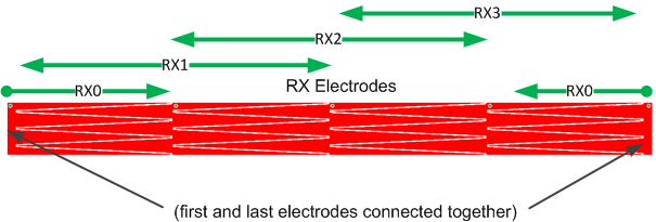
Fig. 51 Example 4-Element Slider Design
Self Capacitive Wheel
A wheel is basically a slider design with both ends wrapped around and connected together. With CapTIvate™ Technology, a self capacitive wheel only needs three elements to provide exceptional linearity and resolution. A basic wheel design below uses three RX channels. Each electrode is inter-digitated.
Fig. 52 Example 3-Element Wheel Design
Mutual Capacitive Sensor Shapes
Mutual capacitance has a unique feature that allows sensors to multiplexed. Mutual capacitive sliders and wheels can take advantage of this feature by sharing several RX channels with one or more sensors. Because of this, it is possible to have up to 64 electrodes using 16 CapTIvate™ I/O pins. As mentioned earlier, mutual capacitive sensor doesn’t have the same sensitivity as a self capacitive slider or wheel. However, with CapTIvate™ Technology, mutual capacitive sliders and wheels will provide the same performance as self capacitive sensors.
Mutual Capacitive Slider
The following diagram illustrates a four element slider. The outer TX electrode traces surround the inter-digitated RX electrodes and are connected together at both ends of the slider. This simple slider design uses four RX and one TX channels.
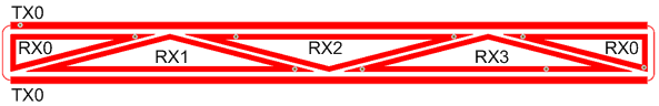
Fig. 53 4 Element Slider Design
TX on outside (track on top and bottom)
RX on inside as triangles
Spacing from TX to RX is 1/2 the overlay thickness
1st and last RX triangle connected to each other
Spacing between TX and RX ~0.5mm
Mutual Capacitive Wheel
The diagram below illustrates a basic 3 element wheel design. The wheel has two TX circle electrodes surrounding the inter-digitated RX electrodes. The wheel is basically a slider design with both ends wrapped around and connected together. This wheel design uses three RX and one TX channels.
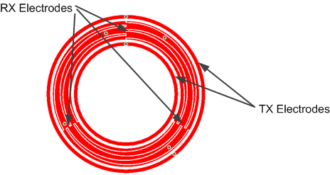
Fig. 54 3 Element Wheel Design
TX Circles on outside and inside of wheel (Need to connect inside and outside together on backside of board)
RX as inter-digitated patterns (similar to Self Capacitance Wheel)
Spacing between TX and RX ~1/2 overlay thickness
Ground hatch added inside wheel to provide noise stability. Also ok to have hatching on backside of board. (be careful of total ground loading
Possible to include LED/LED backlight in the center
Difficult to draw
Touchpads
Capacitive sensing technology is a low cost, low power HMI solution being adopted more and more in wearable and hand held products, such as earbuds, headphones, entertainment remotes and VR (virtual reality) hand controllers. The 2D touchpad is a class of capacitive sensors that provide both gesture and XY finger position. Touchpads are typically square or round, but custom shapes are possible. Hand-held products can augment their traditional button or keypad control experience with a touchpad that provides precision XY finger control using a thumb or finger. Wearable products can incorporate a touchpad as a multi-function user input with finger gesturing to control music volume, song selection, pause and play with simple swipe and tap like gestures.
Fig. 55 Example Remote Control with Touchpad
Getting Started
The guidelines presented this section provide only a basic design overview and general recommendations. To ensure a successful sensor design, it is highly recommended to see application note SLAA944 “Designing a trackpad with MSP430 capacitive touch technology” to better understand how a touchpad sensor works, how to select the optimal design for your application and to be aware of the design limitations.
Topics
The section of the CapTIvate design guide covers the following Touchpad topics:
-
Standard
Basic
-
Shapes
Electrode Pitch
Electrode Spacing
How to create sensor patterns
-
PCB Layout and Routing
FR4
FPC
Overlay
Terminology
RX or TX electrode = Row or column of diamonds connected to MCU’s CapTIvate IO pins
CAPT IO = Capacitive touch pin
Measurement node = Intersection between RX and TX electrode
Sensor configuration = RX/TX electrode pairs (ex. 4x4 configuration has 4 RX and 4 TX connections)
FR4 = Glass-reinforced epoxy laminate material for PCB substrate
FPC = Flexible PCB
ITO = Indium tin oxide is a transparent thin film conductor
CapTIvate Touchpad Technology Overview
CapTIvate Touchpads are mutual capacitive 2D sensors created by the intersection of rows and columns of diamond shaped patterns referred to as RX and TX electrodes. The diamond pattern provides optimal coupling between the RX and TX electrode and is typically made of copper, as on FR4 rigid and Flex PCBs, or ITO for glass substrates. In the illustration below, the intersection of the 4 RX electrodes and 4 TX electrodes create 16 measurement nodes. When a finger touches the surface, the processing algorithm determines the position of the finger based on the relative change in capacitance at each measurement node. Programmable parameters related to how long the finger touches, the number of touches and touch positions are used by the gesture processing algorithm after each measurement to determine if a Tap, Double-Tap, TapHold, or Swipe (up,down,left,right) has occurred. The XY position and gesture data is available to be read by a host MCU.
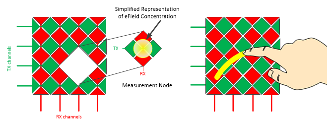
Fig. 56 Touchpad Electrodes
Touchpad Designs
Touchpads can be designed in a variety of sizes, shapes and with lesser or greater XY precision. Applications requiring a greater precision use many RX and TX electrodes to improve the resolution of the measurements, whereas simple gesturing applications don’t need the resolution and can work with fewer RX and TX electrodes. What does your application need? Before starting a touchpad design, let’s briefly look at the two types of touchpad designs and the MSP430 MCUs that support them.
In this document touchpads are referred to as standard or basic. A standard touchpad design solution is expected to provide the performance and features to meet both precision XY finger tracking, as well as gesturing requirements, whereas a basic touchpad design provides a cost sensitive solution for simple gesture applications. The differences are summarized below.
A Standard Touchpad
CapTIvate Touchpad designs offer best in class XY position resolution and precision, with gesturing.
These are applications requiring precision tracking performance, such as game or VR applications
Require MSP430 CapTIvate MCUs with more CAPT IO (channels) and larger memory configurations
Fig. 57 Standard Touchpad MCUs
A Basic Touchpad
A basic CapTIvate Touchpad is a lower cost solution for applications used primarily for gesturing only.
Hand-held remote control or wearable devices
Lower XY precision
Can be implemented on MSP430 CapTIvate MCUs with smaller pin-count and lower memory options
Supports smaller touch areas with 2x2, 3x3 and 4x4 configurations (up to 16 measurement points)
Fig. 58 Basic Touchpad MCUs
Sensor Design
Shapes
Electrode Pitch
Electrode Spacing
How to Generate Sensor Pattern
Shapes
Generally defined by the product requirements, touchpads are commonly square (rectangular) or round. Custom shapes are possible by using the .dxf output of the desired shape rendered in a CAD program. Refer to section Create the Touchpad PCB Sensor.
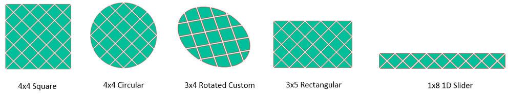
Fig. 59 Common Shapes
Electrode Pitch
A sensor’s pitch is the measured distance from the center of one diamond to the center of a neighboring diamond as shown here. A sensor with smaller pitch will generally have better precision and linearity. A typical electrode pitch is in the range of 3mm to 7mm for a standard touchpad application and 10mm or more for basic touchpad gesturing applications.
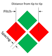
Fig. 60 Electrode Pitch and Spacing
Electrode Spacing
The spacing between the diamond patterns determines the quality of the coupling between an RX and TX diamond. The smaller the spacing, the more tightly coupled the e-field between the diamonds becomes, minimizing crosstalk between channels and improving the sensor’s SNR.
Smaller spacing creates strong coupling with good signal SNR
Larger spacing reduces the signal SNR and degrades cross-talk with neighboring electrodes causing proximity effects
Recommended spacing is 0.1mm (min) to 0.3mm (typical), up to 0.5mm (max) with thicker overlays.
Creating the Touchpad PCB Sensor
PCB
Layout
Routing
Layer Stack
Ground Pours
PCB Layout and Routing
Care must be taken when routing the RX and TX traces from the sensor’s electrodes to the MCU. To avoid unwanted interaction between RX and TX traces always keep the RX and TX traces grouped separately an as far apart from each other as possible. If touchpad signal traces route near a ground trace or ground pour, maintain a gap of 0.5mm or more between the ground pour and electrodes.
Stack Up
Touchpads are typically implemented on 2 to 6 layer FR4 and 2 layer FPC. It is also possible to implement a touchpad on ITO substrates, but is highly recommended to work with an ITO vendor that can advise on the layout.
2 Layer Designs
L1 Electrode
L2 Ground Pour
On a 2 layer design, the MCU and other components should not placed on the layer directly under the sensor. The area on the lower layer under the touchpad sensor is reserved for the ground pour so do not place components in this area. On 2 layer FR4 designs, use a 25% filled hatched pour and on 2 layer FPC designs, use a 10% filled hatched pour.
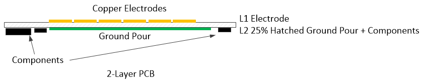
Fig. 61 2-Layer Stack up
Multi-Layer
L1 Electrode
L2 Electrode Traces
L3 Ground Pour
L4 Components
On a multi-layer design, the MCU and other components can be mounted directly under the sensor provided there is a 25% filled hatched ground pour on layer 3 (preferred), or a 10% filled hatched ground pour on L2.
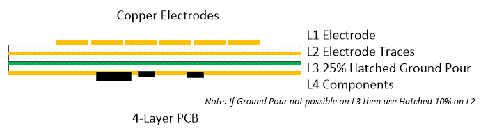
Fig. 62 4-Layer Stack up
Ground Pours
A ground pour is an important part of the touchpad sensor, as it provides a stable ground reference for the sensor measurements and is needed to shield the touchpad sensor potential noise sources from the lower layers on the PCB. To minimize parasitic capacitances, which can affect the sensor’s sensitivity, on FR4 PCB designs always use a hatched ground pour that is around 10 - 25%, depending on which layer (see comments above). On FPC designs, the layers are much closer together, which increases the parasitic capacitance between the electrodes and ground pour on the opposite layer. This increased parasitic capacitance will reduce the sensor’s sensitivity so it is recommended to use a 10% filled hatched ground. ITO designs typically do not include a hatched ground.
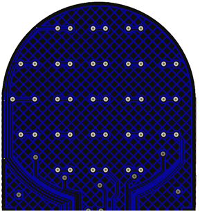
Fig. 63 Example 25% Filled Ground Pour
Touchpad Overlay
The overlay is a very important part of the capacitive touch sensor design and can impact the overall performance. The recommended overlay thickness ranges from 1 to 3mm. The overlay material must be non-conductive, such as plastic or glass.
Proximity
Proximity sensors are electrodes designed to detect a hand or other conductive object at some distance using greater sensitivity compared to buttons, sliders or wheels. For this reason, proximity sensors are recommended to use self capacitive mode and can have one or more electrodes. By having the proximity sensor in your design can reduce the system power consumption and provide the feedback to human interact.
Proximity Design Considerations
The sensing range of a proximity sensor is dependent upon several factors:
The size and shape of the proximity sensor
The proximity range increases with the larger sensor size.
The proximity range also affect by the area of the object approaching to the sensor.
The shape of sensor is most limited by end product and it varies from a solid rectangular pad to a piece of wire.
The sensor configuration tuning values
The proximity range increases with higher sensitivity tuning values.
The values include conversion count, conversion gain, and proximity threshold.
The surrounding conductors
The proximity range increases with increasing the separation of the sensor from other conductors, such as ground.
The system surrounding environment
Increasing the sensitivity of the proximity sensor will also enlarge the effects of noise, temperature drifts and humidity drift to the system.
Overall, proximity sensor design involves carefully balancing sensor size, sensor configuration, ground shielding and system stability.
Proximity Ground and Shielding
Electric Field Propagation
As with any self-capacitive sensor, an isotropic electric field is generated from the electrode and is projected in all directions. The field lines will flow from the electrode to any nearby ground potential and can include a nearby hand or earth ground. This means a hand can approach the sensor from any angle and interact with the E-field. If proximity detection is undesirable from the back or the side of the device, this could easily be prevented by manipulating the direction of the E-field’s projection using different shield implementation methods.
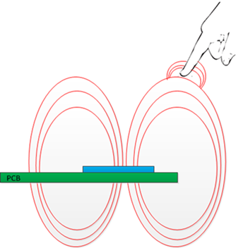
Fig. 64 PCB with Minimal Parasitic Capacitances
Proximity Sensor with No Shield
A proximity sensor without any shielding mechanism can be fully functional, but only applicable if detection from any angle can be permitted. In comparison with other implementation methods, having no shield provides high sensitivity, yielding a long range of sensing distance in 360 degrees. Unfortunately, it is almost impossible to avoid having some ground structures on a PCB or in the product. The presence of these ground structures leads to increase parasitic loading on the sensor, which reduces the percentage change in capacitance when a user approaches the sensor. This leads to a reduction in the sensor’s sensitivity and, ultimately, the detection distance. The proximity electrode on the CAPTIVATE-BSWP board is an example of a sensor without significant shielding.
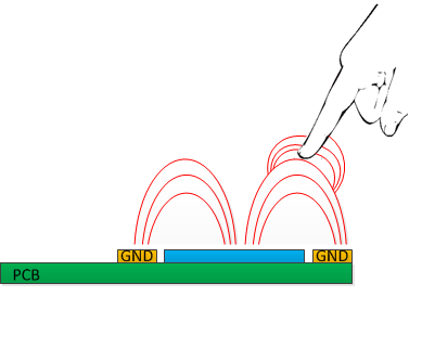
Fig. 65 PCB with Typical Parasitic Capacitances
Proximity Sensor with Ground Shield
A proximity sensor with a ground shield is the best implementation method if the goal is to completely obstruct the E-fields projecting towards the back of the electrode. However, utilizing this method significantly reduces the proximity sensor’s range of distance as it introduces parasitic capacitance between the two electrodes and reduces the E-field propagation out into the desired sensing area. The proximity electrode on the CAPTIVATE-PHONE board is an example of a sensor with ground shielding.
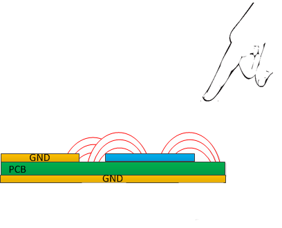
Fig. 66 PCB with Large Parasitic Capacitances
Proximity Sensor with Driven Shield
One method to control the amount of parasitic capacitance to nearby ground while maintaining adequate sensitivity is through the use of a driven shield. A driven shield can be implemented by placing a conductive plane directly under the proximity electrode (separated by insulation) and driving it with a signal identical to the signal driving the sensor.
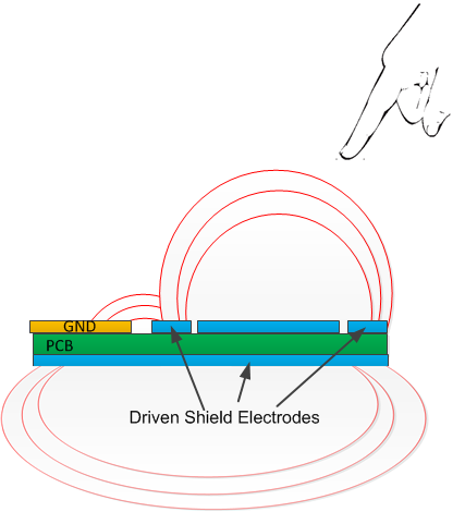
Fig. 67 PCB with Proximity Driven Shield
If the signals driving both the sensor and shield are in-phase and of the same potential, there will be an absence of an electric field between the two electrodes. Furthermore, the shield’s electric field will repel the sensor’s electric field towards the front of the sensor, providing a fair amount of shielding. As a result, this method greatly restores the sensor’s sensitivity and SNR by minimizing parasitic capacitance.
As shown below, an operational amplifier configured as a voltage-follower buffer is required to drive the shield with a signal identical to the signal driving the sensor. A buffer must be used to continuously supply ample current to the shield to maintain a potential difference of zero between the sensor and the shield elements. As the oscilloscope shot shows that the drive signals for the sensor and the shield are identical.
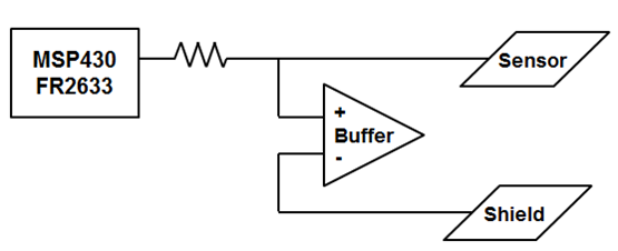
Fig. 68 Driven Shield Configuration
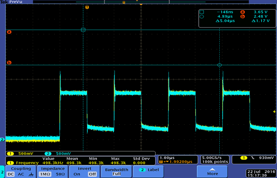
Fig. 69 Oscilloscope Shot of Signals Driving Sensor and Shield
The Texas Instruments OPA354 operational amplifier is the recommended IC for this application. The primary requirements for the op-amp are rail-to-rail drive capability, a high slew rate, and high input impedance. The input impedance should consist of a large resistance and a very low common-mode capacitance to ground. The OPA354 has a slew rate of 150V/µs and an input impedance of approximately 10^13Ω in parallel with 2pF of capacitance. The trade-off of using this implementation is higher BOM cost and increased power consumption.
The graph below shows how the three different implementation methods (ground shield, driven shield, and no shield) respond to approaches above and below the sensor. Data was collected for each variation of shields by holding a 15.2cm x 10.2cm grounded copper plate (simulating a hand) approximately 3cm over and under a sensor board (shown below) with a 4.6cm x 3.8cm sensor electrode. The measurement delta was obtained using the CapTIvate Design Center GUI. Comparing the driven shield data to the ground shield, the MCU is still able to detect a small change in capacitance caused by an object 3cm under the proximity sensor but is able to deliver approximately 7 times the sensitivity from the front. An easy solution to completely eliminate detection from the back is placing an additional grounded shield under the driven shield. Adding the ground shield will not weaken the proximity sensor’s sensitivity.
Proximity Range Test
Below are proximity range test results with two different CapTIvate MCUs boards, five different sensor board designs and two different copper plate designs.These results may be used as a reference for estimating the proximity distances which are achievable with different sensor geometries. The two copper plate designs (simulating a flat hand and an outstretched finger) were mounted on a robust moving metal rod structure. This provided an accurate test system to collect proximity range data without the interference of objects around the sensor. The proximity range setup is shown below:
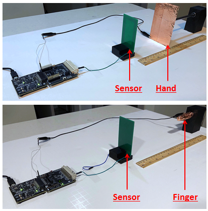
Fig. 70 Proximity Range Test Setup
CapTIvate MCUs boards:
First-Generation Device: MSP430FR2633 MCU Board
Second-Generation Device: MSP430FR2676 MCU Board
Sensor Board Layouts:
Sensor 1 is a 80mm by 50mm solid rectangular shape with no ground
Sensor 2 is a 60mm by 30mm solid rectangular shape with no ground
Sensor 3 is a 80mm by 50mm with 10mm wide rectangular ring shape with no ground
Sensor 4 is a 80mm by 50mm with 10mm wide rectangular ring shape with a center hatched ground
Sensor 5 is a 80mm by 50mm with 10mm wide rectangular ring shape with a full back hatched ground
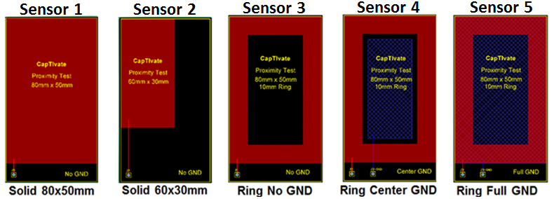
Fig. 71 Proximity Range Test PCB Layouts
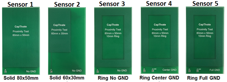
Fig. 72 Proximity Range Test Hardware
CapTIvate Design Center Inputs and SNR results:
The Conversion Count was set to 500, and the Conversion Gain was set to 100
The proximity and touch threshold values were based on the minimum recommended values for both the first-generation and second-generation CapTIvate devices under different operating temperatures. For more details on this process, see the application report Sensitivity, SNR, and Design Margin in Capacitive Touch Applications.
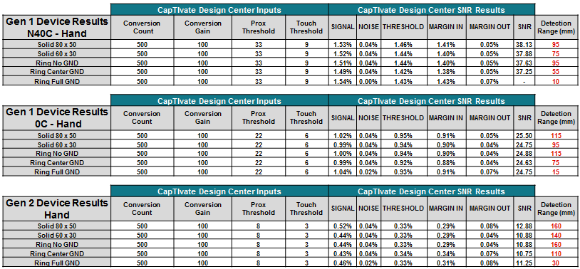
Fig. 73 Proximity Range Test PCB Layouts
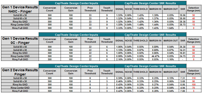
Fig. 74 Proximity Range Test PCB Layouts
Summary of Proximity Range Test Results:
The graphs below show a visual representation of the proximity range data for different sensors, approaching object sizes, and CapTIvate MCUs.
Factors which influence detection range:
Detection range increases with larger sensor size
Detection range increases with separation of sensor from GND
Detection range increases with larger approaching object size
Detection range increases with higher CapTIvate sensitivity tuning values
The Gen 2 device provides more detection range because it has a lower maximum device noise floor, which allows for lower proximity and touch threshold values
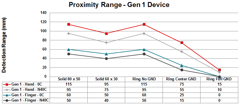
Fig. 75 Proximity Range Test Results With Change of Conversion Count
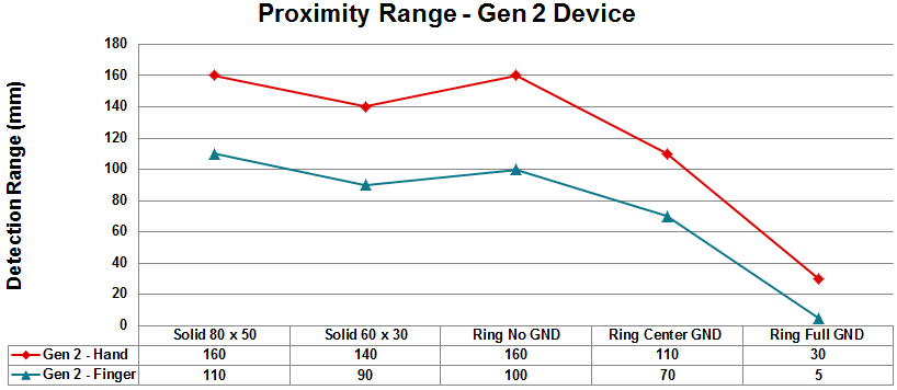
Fig. 76 Proximity Range Test Results With Change of Conversion Count
Metal Touch
Compared to traditional capacitive sensing through plastics or glass, capacitive metal touch is only sensitive to an applied force and for this reason is an excellent choice for harsh or hostile environments where there are liquids, grease, mud or grime present and environments where a user may be wearing gloves. The principle of measuring the capacitance is straight forward for metal touch applications as the deflection in the grounded metal overlay causes a change in the capacitance between the electrodes and the metal overlay.
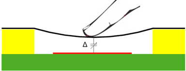
Fig. 77 pcb
Design Considerations
The mechanical stackup plays an important role as it will ultimately determine the sensitivity and quality of user experience. There are many design factors to consider, such as the thickness of the metal overlay, the size of the electrode, what type of bonding material, thickness and technique, etc.
For design assistance, refer to the CapTIvate™ Metal Touch application notes and metal deflection tool located at https://www.ti.com/captivate
Transparent Touch
For applications that incorporates capacitive-touch technology in a HMI designs as touch sensors over liquid crystal displays (LCDs), optically transparent sensors are required. And most transparent capacitive-touch sensors are built using indium tin oxide (ITO).
Indium Tin Oxide (ITO)
Indium Tin Oxide (ITO) is a transparent conductor sputtered onto a substrate such as glass or plastic. Once the substrate has been coated with ITO, a pattern can be etched using a variety of processes.
Fig. 78 ITO_1
Because ITO is a optical transparent material so the stack up of the ITO capacitive touch sensor is different from a traditional copper sensors like the below graph shows.
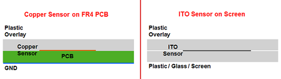
Fig. 79 ITO Stack Up 1
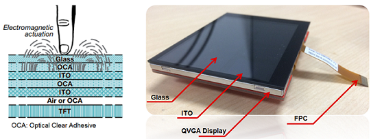
Fig. 80 ITO Stack Up 2
There are many advantages over a full-featured touchscreen solution by using CapTIvate technology with ITO sensors:
Lower system cost
Shorter development time
Higher reliability
Lower power consumption
Proximity sensing feature
Preserving durability
To learn more about ITO capacitive touch sensor with CapTIvate technology please refer to:
White Paper: https://www.ti.com/lit/wp/sway006/sway006.pdf
Demo Video: https://www.ti.com/product/MSP430FR2633/support
Ultra Low Power
The MSP430 CapTIvate™ peripheral is capable of enabling user interface designs with extremely low power consumption. This is possible because the CapTIvate™ peripheral includes a processing state machine that is capable of performing the following functions from LPM3 without any CPU interaction whatsoever:
Wake up the CapTIvate measurement blocks from deep sleep (LPM3) at a periodic interval
Start a conversion automatically (1 electrode per measurement block, or 4 electrodes on the MSP430FR2633)
Finish the conversion
Perform IIR noise filtering (adjustable strength)
Perform a threshold crossing detection (adjustable window comparator)
If a threshold was crossed, wake up the CPU
Otherwise, perform environmental drift compensation (adjustable strength)
Shut down the CapTIvate measurement blocks and wait until the next interval, then go back to #1
This capability combined with the MSP430 FRAM low power architecture enables designs with average current in the single digit microamps.
Introduction
Designing for low power consumption involves optimizing the hardware and the tuning to achieve 5 basic things:
The lowest base LPM3 current possible
The slowest UI refresh rate possible (software design)
The smallest parasitic capacitance possible (hardware design)
The shortest measurement time possible (hardware and software design)
The most effective use of the wake-on-proximity state machine
In short, achieving the lowest possible power consumption is all about optimizing the duty cycle of the application - minimizing the amount of time that the CPU and high performance analog are awake, and maximizing the amount of time spent in deep sleep.
Expectations
Below are several test cases that have been bench verified with the MSP430FR2633 on the CAPTIVATE-FR2633 processor module.
Sensor Configuration |
Mode |
Method |
Scan Rate |
Base Scan Time |
LF Clock |
I-avg |
I-avg / Electrode |
Years on AAAs |
Years on a CR2032 |
|---|---|---|---|---|---|---|---|---|---|
1 Proximity Sensor |
Wake-on-Proximity |
Self |
8 Hz |
420us |
Crystal |
5uA |
5uA |
16 |
3.6 |
1 Proximity Sensor |
Active (CPU) |
Self |
8 Hz |
420us |
Crystal |
7.3uA |
7.3uA |
10.9 |
2.5 |
1 Button |
Wake-on-Proximity |
Self |
8 Hz |
145us |
Crystal |
3.4uA |
3.4uA |
23.5 |
5.3 |
1 Button |
Active (CPU) |
Self |
8 Hz |
145us |
Crystal |
6.0uA |
6.0uA |
13.3 |
3.0 |
4 Buttons |
Wake-on-Proximity |
Self |
8 Hz |
120us |
Crystal |
3.0uA |
750nA |
26 |
6.0 |
4 Buttons |
Wake-on-Proximity |
Self |
8 Hz |
145us |
Crystal |
3.8uA |
0.9uA |
21 |
4.7 |
4 Buttons |
Wake-on-Proximity |
Self |
30 Hz |
145us |
Crystal |
9.4uA |
2.4uA |
8.5 |
1.9 |
4 Buttons |
Active (CPU) |
Self |
8 Hz |
145us |
Crystal |
8.7uA |
2.2uA |
9.2 |
2.1 |
8 Buttons |
Active (CPU) |
Self |
8 Hz |
145us |
Crystal |
14.5uA |
1.8uA |
5.5 |
1.2 |
8 Buttons |
Active (CPU) |
Self |
15 Hz |
145us |
Crystal |
25.9uA |
3.2uA |
3.0 |
0.7 |
8 Buttons |
Active (CPU) |
Self |
30 Hz |
145us |
Crystal |
50.1uA |
6.3uA |
1.5 |
0.3 |
64 Buttons |
Active (CPU) |
Mutual |
8 Hz |
145us |
Crystal |
109.2uA |
1.7uA |
0.7 |
0.2 |
64 Buttons |
Active (CPU) |
Mutual |
15 Hz |
145us |
Crystal |
203.5uA |
3.0uA |
0.35 |
0.08 |
Note: These measurements were captured using a high resolution source-meter with UART/I2C communications disabled. Battery life was approximated assuming 1000mAh AAA’s and 225mAh CR2032 cells with 70% effective usable life.
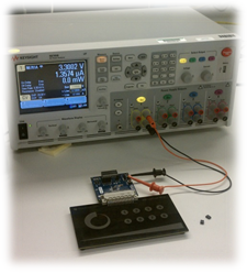
Fig. 81 Power Characterization Bench
Note how the wake-on-proximity state machine is able to increase the battery life by over a year on a CR2032 coin cell for the proximity sensor, and over 2 years for a basic button.
Optimization Steps
The following sections discuss how to optimize the design to achieve the 5 goals introduced above.
Selecting a Low Frequency Clock
The lowest power consumption achievable is limited by the deep sleep current consumption of the MCU. From there, power consumption will rise with the complexity of the panel and rate at which the panel is scanned. In deep sleep (low power mode 3), since it is not possible to achieve a lower average current than the LPM3 current, the low frequency clock that is selected for the application must be considered. Below are the low frequency clock options available for the MSP430FR2633 MCU.
LF Clock Source |
Typical LPM3 Base Current |
Typical Frequency |
Typical Relative Accuracy |
Typical Relative Cost |
|---|---|---|---|---|
Crystal |
1.2uA |
32768 Hz |
Best |
External Component (Highest) |
REFO |
16uA |
32768 Hz |
Good |
Internal (Lowest) |
VLO |
1uA |
10000 Hz |
Poor |
Internal (Lowest) |
If budget and PCB space constraints allow for it, an external 32 kHz crystal provides the best combination of accuracy and low power.
If accuracy is still required but an external crystal cannot be used, then the REFO will provide a decent 32 kHz time base at the expense of higher power consumption.
If an external crystal cannot be used and accuracy is not application critical, than the VLO provides the lowest possible power.
Using the VLO in Wake-on-Proximity Mode
The CAPT_App layer of the Starter Project contains a provision for using the VLO as the clock source to the CapTIvate timer. This may be desirable for applications that require very low power but cannot use a crystal for some reason. When the VLO is used as the clock source for the CapTIvate timer, it is possible to run CapTIvate’s wake-on-proximity mode while in LPM4, rather than the typical LPM3. When in LPM4, ACLK is turned off completely. This means that if the REFO was the ACLK source, the REFO will also be shut down in LPM4, lowering average power consumption. To enable the VLO+LPM4 combination when in wake-on-proximity mode, go to controller properties and check the Force LPM4 in Wake-on-Prox Mode box. This will cause the application low power mode to switch to LPM4 when in the wake-on-proximity state. It will also set up the CapTIvate timer to run off of the VLO when in the wake-on-proximity state. Once the application wakes back up and the UI switches to active mode, ACLK and LPM3 will again be used to ensure timing accuracy.
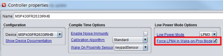
Fig. 82 Force LPM4 in Wake-on-Prox Mode
While the VLO can provide low power consumption without the use of a crystal, it is not as accurate as a crystal. Designers should be aware that the VLO clock frequency can drift considerably with voltage and temperature. See the device specific datasheet for more details. The variance in the VLO clock frequency can show up as a change in the response time of the application. For example, of the frequency drifts low, CapTIvate touch sensors may take longer than usual to respond. Likewise, if the frequency drifts high, sensors may respond faster than usual. In the second case, the power consumption may also be higher than expected because the sensors are being measured more frequently than intended. It is possible to improve the usage of the VLO by implementing a calibration routine that trims the scan interval setting by comparing the VLO to a more accurate clock (such as the REFO).
Optimizing the Application Scan Period
The application scan period is the amount of time between each sampling of the user interface. For example, if the period is set to 100ms, then the user interface is sampled every 100ms, or at a rate of 10Hz. If the period is set to 10ms, then the user interface is sampled at a rate of 100Hz. The scan period has a direct effect on the power consumption, as it controls the duty cycle of the application. When a lower period (higher rate) is selected, the CapTIvate analog and possibly the CPU are waking up much more frequently- consuming more power. The design tradeoff here is response time versus power consumption. Scanning less often reduces the power consumption, but also increases the response time of the user interface. The CapTIvate™ starter project implements an active mode scan rate and a wake-on-proximity scan rate. This allows for a longer response time to be used when no one is touching the panel, and a shorter response time to be used when someone is touching the panel. The CAPTIVATE-BSWP demo panel runs at 10 Hz (100ms response time) when in wake-on-proximity mode, and at 30 Hz (33ms response time) when in active mode.
Optimizing for the Smallest Parasitic Capacitance
When a sensor has a low parasitic capacitance, it is more sensitive to touch (all else being equal). This means that the sensor may be scanned at a lower resolution to obtain the same resolution and SNR. A lower resolution conversion means a lower measurement time. Battery powered applications typically do not have the same noise immunity requirements as line powered applications, so solid ground fills that limit sensitivity are generally not required. In addition, when sensors have low parasitic capacitance the conversion frequency may be increased while still ensuring good charge transfer.
Optimizing for the Shortest Measurement Time
The measurement time for each sensor should be optimized to be as small as possible. When the CapTIvate™ analog IP is operational, it draws several 100uA of current. The goal should be to minimize the measurement time so that the analog is only enabled for a brief period of time.
In the CapTIvate™ Design Center, the measurement time is a function of the following factors:
Frequency Divider (Conversion clock frequency selection)
Conversion Count (Base number of charge transfers without a touch)
The measurement time may be calculated manually per the following formula. It is also calculated automatically in the CapTIvate™ Design Center.
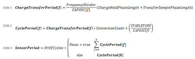
Fig. 83 Scan Time Calculation
Constants
STABLETIME=320
CAPOSC[0]=16000000
CAPOSC[1]=14700000
CAPOSC[2]=13100000
CAPOSC[3]=11200000
If the sensors have fairly low parasitic capacitance, a conversion frequency of 2MHz for self capacitance and 4MHz for mutual capacitance is a reasonable setting. With phase lengths of 1, this is achieved by setting the frequency divider to /4 and /2, respectively.
The conversion count controls the resolution of the measurement. Decreasing this value decreases the overall resolution of the measurement (in terms of counts per picofarad). To optimize the resolution, decrease this value until the minimum acceptable delta due to a touch is reached.
Using the Wake-on-Proximity State Machine Effectively
The wake-on-proximity state machine allows for CPU-less measurement and processing for 1 element per measurement block (4 elements total with the MSP430FR2633). Most sensing panels are actually touched <1% of the total time that they are running. 99% or more of the time, they are waiting for a user. The state machine provides a mechanism to handle the latter 99% without the need to involve the CPU, reducing the average current. A sensor may be selected as a wake-on-proximity sensor in the CapTIvate™ Design Center. When a sensor is selected, the starter project that is generated by the CapTIvate™ Design Center will transition into a wake-on-proximity mode whenever the inactivity timeout counter expires. In wake-on-proximity mode, the first cycle of the sensor that was selected for wake-on-proximity will be automatically measured by the state machine, and the CPU will not receive an interrupt until one of the following occurs:
A proximity or negative touch threshold crossing occurs
A conversion counter interrupt occurs
The wake-on-proximity feature is best used with longer-range proximity sensors, such as the one on the CAPTIVATE-BSWP demo panel. However, if an MSP430FR2633 design has 4 buttons or less, it is possible to use the wake-on-proximity state machine functionality to wake up on any of the four buttons!
Walking Through the Optimization Process
In this example, the CAPTIVATE-BSWP panel will be used as a piece of test hardware to look at how to optimize an imaginary application that has 4 buttons. From start to finish, going through this exercise will transform the average current of the solution from 100’s of microamps to single digit microamps. To run the completed example, check out the UltraLowPower_4Button example project.
Step 1: Creating a New Project
To start, a new CapTIvate™ Design Center project will be created that has a button group sensor with 4 buttons. The buttons will be on CAP0.0, CAP1.0, CAP2.0, and CAP3.0. This mapping allows for parallel scanning, which is important for power optimization. All of the default tuning parameters will be kept initially:
Parameter |
Value |
Optimized? |
|---|---|---|
COMM Peripheral |
UART |
No |
Active Scan Rate |
33 |
No |
Wake-on-Proximity Scan Rate |
N/A |
No |
Conversion Count |
500 |
No |
Frequency Divider |
f/4 |
Yes |
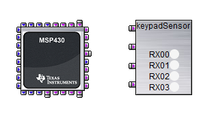
Fig. 84 Design Center Configuration
Out of all the default configuration values, only the frequency divider is optimized (f/4 with phase lengths of 1 for a conversion frequency of 2 MHz). This yields a starting, un-optimized current of approximately 310 uA-avg. We can do better than this! Note that LED1 and LED2 of the CAPTIVATE-FR2633 processor module must be disconnected, or the measured power will be higher.
Step 2: Switch from UART to I2C
UART requires that SMCLK be active for the baud rate generator to work. By switching to I2C for data transfer, we are able to go to LPM3 instead OF LPM0. This is possible because as a slave, the MSP does not need to provide a clock for I2C to operate.
Parameter |
Value |
Optimized? |
|---|---|---|
COMM Peripheral |
Bulk-I2C (Slave) |
Yes |
Low Power Mode |
LPM3 |
Yes |
Active Scan Rate |
33 |
No |
Wake-on-Proximity Scan Rate |
N/A |
No |
Conversion Count |
500 |
No |
Frequency Divider |
f/4 |
Yes |
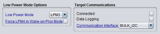
Fig. 85 Design Center Configuration
Making this change has lowered the current to 68 uA-avg. We can still do better! Note that the Design Center must be connected to see these power numbers, otherwise the I2C requests will time out, using more power.
Step 3: Optimize the Conversion Count
The project came with a default conversion count of 500. This provides a delta due to touch of about 80 on the 4 buttons. This is more resolution than is needed. Lowering the conversion count to 200 and the conversion gain to 100 (to boost sensitivity) will cut the measurement time more than in half, and still provide a delta of about 30 counts. 30 counts is significantly less, but for button detection in a battery powered application, it is adequate. The default touch thresholds still work as well.
Parameter |
Value |
Optimized? |
|---|---|---|
COMM Peripheral |
Bulk-I2C (Slave) |
Yes |
Active Scan Rate |
33 |
No |
Wake-on-Proximity Scan Rate |
N/A |
No |
Conversion Count |
200 |
Yes |
Frequency Divider |
f/4 |
Yes |
These changes lower the current to 38 uA-avg. We are getting there.
Step 4: Adjusting the Active Mode Scan Period
The default scan period of 33ms provides good response time, but it uses power. Adjusting this down to 83ms (12 Hz) will reduce the power, but not so much that it compromises the ability to pick up a press.
Parameter |
Value |
Optimized? |
|---|---|---|
COMM Peripheral |
Bulk-I2C (Slave) |
Yes |
Active Scan Rate |
83 |
Yes |
Wake-on-Proximity Scan Rate |
N/A |
No |
Conversion Count |
200 |
Yes |
Frequency Divider |
f/4 |
Yes |
This change lowered the current to 26 uA-avg.
Step 5: Enabling and Adjusting the Wake-on-Proximity Mode
Now to add the final touches, let’s enable the wake-on-proximity state machine functionality to manage states. We only have 4 buttons, with one from each measurement block, so we can measure all 4 buttons and test for proximity without any CPU involvement.
Parameter |
Value |
Optimized? |
|---|---|---|
COMM Peripheral |
Bulk-I2C (Slave) |
Yes |
Low Power Mode |
LPM3 |
Yes |
Active Scan Rate |
83 |
Yes |
Wake-on-Proximity Scan Rate |
125 |
Yes |
Conversion Count |
200 |
Yes |
Frequency Divider |
f/4 |
Yes |
The capture below shows the conversion control tab of the controller customizer, which contains most of the settings that we have been adjusting to optimize for low power.
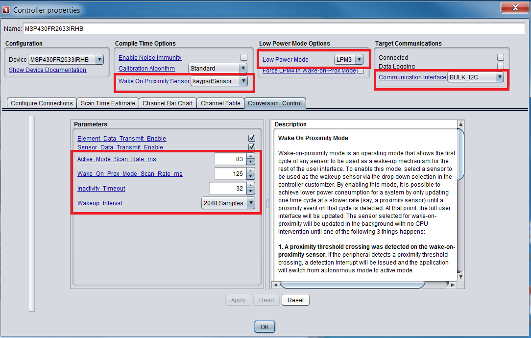
Fig. 86 Lower Power Settings
This change lowered the current to 3 uA-avg, or about 750nA per button when no one is touching the panel. As soon as a user touches a button, the power consumption goes up to 23-26uA-avg with I2C reporting. Once the touch is removed, the UI goes back into wake-on-proximity mode after 32 samples and is back to the 3 uA-avg.
A Note about Mutual Capacitance and Bias Current
Mutual capacitance sensors have an extra tuning parameter: the bias current. During a mutual capacitance measurement, a sample-and-hold amplifier cancels out the effects of the parasitic / stray self capacitance on the receive electrode. This sample-and-hold amplifier has an adjustable bias current capability, which allows for the drive strength of the amplifier to be adjusted to suite the application.
For information on bias current settings how to adjust the bias current, see the bias current guide. Note that the bias current control is only available in advanced mode.
A larger bias current setting should be used when the parasitic capacitance to ground of the Rx electrode is large. The default value is the highest possible bias current, which works for the most applications but requires the highest power consumption. During low power optimization, it is desirable to lower the bias current if the layout allows for it. Most button designs with minimal parasitic capacitance work very well with the lowest bias current setting.
Bias Current Optimization Procedure
To optimize the bias current setting for a low power application, begin by setting the bias current to the lowest available setting. Test each electrode in the sensor for sensitivity to touch. One effect of setting the bias current too low is that a touch on a sensor will cause a decrease in counts rather than an increase, because the system cannot accurately compensate for the parasitic self capacitance of the receive (Rx) electrode. If this occurs, continue increasing the bias current until the behavior goes away. Note that the bias current performance also varies with the conversion frequency. Higher conversion frequencies will require higher bias current settings for designs with more parasitic capacitance to ground.
Moisture
This section discusses special considerations for designing products that will come into contact with moisture.
Introduction
The performance of a capacitive touch panel can be affected by moisture spray and build-up, as well as liquid spills. In addition, self capacitance and mutual capacitance exhibit different phenomena depending on the nature of the moisture. For example, small water droplets on a self capacitance electrode may have little effect, but a water droplet on a mutual capacitance electrode may have the effect of improving the mutual coupling and creating a change in the measurement counts that goes the opposite direction of a touch. Interestingly still, a water droplet or spill on a self or a mutual capacitance electrode could cause a change in measurement counts in the direction of (rather than against) a touch, if the droplet or spill is also in contact with a nearby ground plane, power plane, or grounded electrode that is not being measured. This section will introduce the physics behind the effects of moisture, as well as some basic best practices to add a level of moisture resistance and detection to an application.
Expectations
With careful attention to detail, it is possible to create designs that can reject small amounts of moisture. Through the use of guard channels, it is also possible to create designs that can detect spills and lock out the rest of the interface when a spill is detected.
Moisture Physics
Moisture build-ups and liquid spills that occur on panels in the real world affect capacitive sensing electrodes because the liquid on the panel exhibits electrical conductivity. Water is a polarized molecule, and in addition to its polarization, it is rarely pure and typically contains ions in solution. The amount of ions dissolved directly effects the conductivity of the moisture. Distilled water will appear to have much less of an effect than salt water or sweat, for example.
This conductive property means that moisture can appear to have a similar effect as placing a conductor (such as a piece of metal) on a panel. It’s easy to understand how that will cause problems! Making things worse is the fact that moisture is unpredictable in multiple aspects:
Its actual conductivity is extremely variable
The shape and size of droplets and spills are unknown and constantly changing
Changes tend to be fast- making them look more like a touch and less like an environmental change
Moisture Problems
At best, build-up of moisture occurs slowly over time and is tracked via environmental filtering. At worst, it happens unpredictably and quickly and triggers a false detection.
Moisture Mitigation Techniques
Because of the unpredictable nature of moisture, it is necessary to divide mitigation techniques into two types of applications: moisture tolerance and spill rejection.
Application Type |
Full Touch Detection |
Spill Detection |
Guard Channel Required |
Typical Mechanical Mounting |
|---|---|---|---|---|
Moisture Tolerance |
Yes, typically |
No |
No |
Vertical |
Spill Detection |
No, sensors are masked during a spill |
Yes |
Typically required |
Horizontal |
Moisture Tolerance Applications
Moisture tolerant applications include those which are able to operate with touch detection in the presence of steam, mist, and spray. Common applications include exterior/interior security panels, E-locks, thermostats, and car access keypads. Whether or not moisture tolerance is feasible for an application depends on the mechanical design and environment. Typically, the following must be true:
The touch sensing panel is installed perpendicular to the earth (vertically or at some angle) such that any moisture that accumulates on the panel will drip away on its own due to gravity
There is no opportunity for moisture/fluids to “pool” or “flood” the sensing panel
Design Tips for Moisture Tolerance
When designing a moisture tolerant application:
Provide as much spacing as possible between buttons
Provide significant spacing between buttons and nearby ground planes
Route all electrode connection traces on the PCB layer furthest from the surface
Set sensor idle states to High-Z (floating) so that nearby sensors don’t provide coupling points that can cause false detections
If possible, use a non-conductive enclosure for the product
Spill Rejection Applications
Spill rejection applications include those which are able to detect when a fluid spill has occurred on the sensing panel. Common applications are white goods such as a cooking surface control panel. The goal of spill rejection is not to enable full touch detection (which is extremely difficult when moisture or fluids cover multiple keys and/or ground), but simply to detect the presence of a spill and lock out the keypad until the spill is cleared by a user. This is most commonly achieved with the use of a guard channel, whose purpose is to detect large objects as well as spills.
Design Tips for Spill Detection
When designing a spill detection application:
Implement a guard channel to detect when a large unknown object or some kind of spill comes into contact with the sensing panel
In software, utilize the guard channel to mask reporting of touches on other keys when a spill is detected.
The CAPTIVATE-PHONE demonstration panel has a guard channel that is used for proximity sensing, palm rejection, and basic moisture rejection.
The Effect of Batteries on Capacitive Touch Systems
This section highlights the differences between a grounded system and a battery powered floating system. The touch-induced change in a sensor’s capacitance is reduced when the capacitive touch module, or the product containing the touch module, does not have an earth ground connection. This is the case in a battery-powered product. This is because of the added capacitance between the battery’s local ground (i.e. the negative terminal of the battery) and the earth ground. This added capacitance decreases the capacitance induced by the user when making contact with the capacitive touch system.
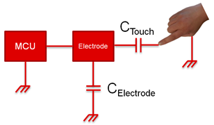
Fig. 87 Model of self mode capacitive touch referenced to earth ground
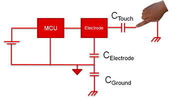
Fig. 88 Model of self mode capacitive touch powered with a battery
Line Power and Battery Test Setup
The difference in sensitivity in a battery-powered configuration was measured was by using the CapTIvate Design Center’s SNR, or signal to noise ratio, test. The test took 250 measurements of the electrode under a touched condition and 250 measurements of the same electrode not being touched and compared the differences to calculate a change in capacitance. A finger probe that was tied to earth ground using a cable connected to the earth of a wall outlet was used to act as a human finger and induce the touch. This was done to have consistent sensor pressure and coverage over all the measurements. The system was lifted off of the ground approximately 4 inches using a plastic box and a piece of foam board to minimize coupling between the system and the grounded lab bench.
The CAPTIVATE-PHONE, CAPTIVATE-BSWP, and EVM430-CAPMINI were used to measure the impact of mutual capacitance, self capacitance, and board size effects on sensitivity reduction. The conversion counts and conversion gains for each board are listed in Table 1 below. Block diagrams and pictures of the setup are shown below using the CAPTIVATE-PHONE board as an example.
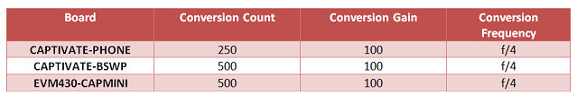
Fig. 89 Line powered vs Battery Performance
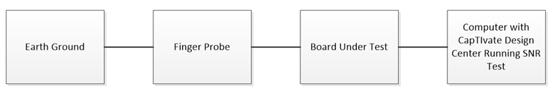
Fig. 90 Block diagram of line powered test setup
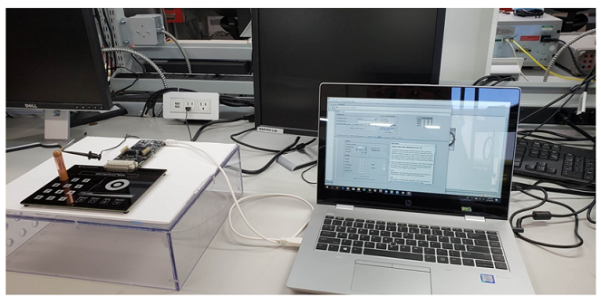
Fig. 91 Line powered test setup
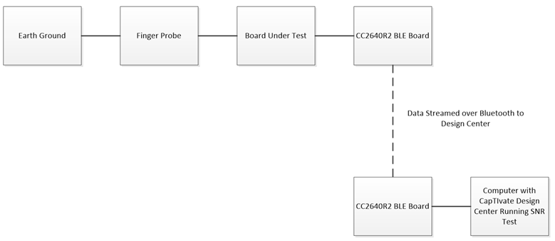
Fig. 92 Block diagram of battery powered test setup
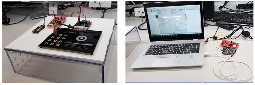
Fig. 93 Battery test setup
Every keypad key was repeatedly tested, and then the measurements were averaged to get an average change in capacitance for a specific key. This was repeated for each board under battery power and wall power referenced to earth ground. For the earth ground tests, the data was connected directly to a laptop via USB and the laptop was plugged into the wall, thus giving the entire system a reference to earth ground. For the battery powered tests, data was streamed over Bluetooth to the CapTIvate Design Center GUI for the measurements to remove the grounding effect caused by the laptop. There was a noticeable decrease in the percent change in capacitance when the system was connected to a battery vs when the system was plugged into the wall; see Table 2. This can be significant when using a system which requires precise capacitive touch sensing.
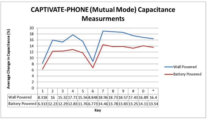
Fig. 94 CAPTIVATE-PHONE Change in button capacitance
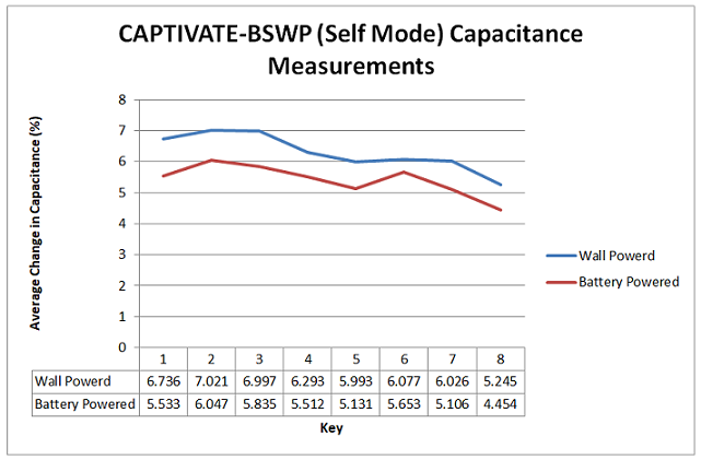
Fig. 95 CAPTIVATE-BSWP Change in button capacitance
There was a trend of a battery powered system having a lower percent change in capacitance than a wall powered system; however the difference was very minute; see Table 2. If extremely precise capacitive touch sensing is required, then it’s possible that this should be taken into account; however in most applications this isn’t large enough to cause issues.
The difference between the percent change in capacitance for battery powered systems and wall powered systems was much more pronounced for mutual mode than self mode. The data comparing mutual mode vs self mode, as well as the percentage reduction of sensitivity between wall power and battery power is listed in Table 2 below
Fig. 96 Line Powered vs Battery Performance
The percent change in capacitance for the CAPMINI differs slightly more than the BSWP board when connected to wall power vs a battery; see Table 3. The average percent change in capacitance for the CAPMINI was larger than the average percent change in capacitance for the BSWP, indicating that a smaller board size slightly increases the sensitivity for self capacitive sensing solutions due to the shorter traces and lower routing parasitic capacitance.
Fig. 97 CAPMINI Change in Button Capacitance
Fig. 98 CAPMINI Line Powered vs Battery Performance
Summary
When designing and testing a system, precaution must be taken when the end product is to be powered by a battery. If using a mutual capacitance sensing system, it has been shown that sensitivity of the system decreases by approximately 23.05% when the system is powered using a battery vs when the system is powered with a reference to earth ground, such as a wall outlet. In the case of self capacitive systems, the difference is smaller for the BSWP board being 14.06%, and slightly larger for the CAPMINI being 24.97%. It is important to take note of this if testing a system with a laptop plugged into the wall for example, but the end product is to be battery powered and suspended in the air.
Recommendations for Design
When testing a system using an earth referenced test setup, increase the conversion count or lower the threshold to increase the sensitivity if the final product is to be battery powered.
System PCB size and where the system is mounted will affect the free space coupling caused by powering the system via battery. Increasing the sensitivity can be achieved by increasing the overall PCB size and increasing the free space coupling
Sensitivity can be improved by enlarging the ground plate on the PCB when powering via battery
Noise Immunity
This section discusses how to design for electromagnetic compatibility.
Introduction
Capacitive touch sensing involves the measurement of very small changes in capacitance of a sensing electrode. These changes are often on the order of a picofarad or less. Because the quantity being measured is so small, capacitive touch circuits that are going to be used in noisy environments must be designed with noise immunity in mind from the start. Often, potential noise sources may not even be known at the time of design. This chapter is dedicated to providing the necessary guidance to enable immunity to various types of noise. It introduces the most common noise threats to a capacitive touch system. For each threat, it discusses how to reduce the susceptibility of a capacitive touch circuit to that threat when using MSP CapTIvate™ MCUs.
How to Use This Section
If you are designing a system that will exist in a high noise environment, it is best to read and understand this guide before going through the process of schematic capture and layout design. It is strongly recommended that the Capacitive Sensing Basics chapter be read before reading this chapter.
The introduction section of the noise immunity guide establishes a knowledge base that will be used as a backdrop for the rest of the discussion. After the introduction, the following section will discuss several different noise problems (RF susceptibility, for example). Each problem will be introduced so that the phenomenon is understood. Finally, the last section will discuss the noise mitigation steps to apply to your design to provide robustness to all of the noise types discussed. The noise mitigation steps will be presented in the context of the Three Sided Approach. The noise mitigation steps section is the most important section.
Noise Mitigation Checklist
The noise mitigation steps section provides a check list of considerations to apply when designing for noise immunity. If you don’t read the entire noise immunity guide, be sure to read the noise mitigation steps.
Additional Resources
In addition to the design documentation here, there are several TI Designs and literature available that demonstrate how to achieve noise immunity:
CapTIvate EMC White Paper: Enabling noise-tolerant capacitive-touch HMIs with MSP CapTIvate technology
CapTIvate EMC Reference Design: Noise Tolerant Capacitive Touch HMI Reference Design TIDM-CAPTOUCHEMCREF
CAPTIVATE-EMC is an evaluation board that enable users to easily evaluate CapTIvate’s electromagnetic compatibility performance relative to their design requirements.
Aggressor-Victim Philosophy
An aggressor-victim approach is taken to understand noise in a system. The diagram below illustrates this concept.
Fig. 99 Aggressor-Victim Diagram
The aggressor is the noise source, which generates interference that affects the victim through the coupling medium. Generally speaking, for noise to couple from the aggressor to affect the victim, the following must be true:
The noise must be at a frequency at which the victim is vulnerable
The noise must have enough amplitude to affect the victim
The noise must be present at a time when the victim is vulnerable to the noise
Aggressor
The aggressor varies with every application. Common aggressors are poorly designed power supplies with high common-mode and differential-mode emissions, long cables and/or traces that act as antennas to radio frequency (RF) signals, and high-current switched inductive loads that share their power source with the victim at some level. In some cases, the viewpoint is such that the capacitive touch circuit is the aggressor.
Coupling Medium
The medium through which the noise travels from the aggressor to the victim is often misunderstood. Common mediums include the VCC rail, the VSS rail, the capacitive coupling between traces (in the case of crosstalk), and even users of the capacitive sensing interface themselves.
Victim
During most of the discussion in this chapter, the capacitive touch circuit is the victim. However, there are times where the capacitive touch circuit becomes the aggressor, at which time a neighboring subsystem may become the victim.
The Three Sided Approach
Based on this understanding, it becomes clear that to reduce the effects of the aggressor on the victim, it is necessary to fulfill one or more of the following objectives:
Change the characteristics of the noise emitted by the aggressor to either change its frequency or reduce its amplitude to a level that does not affect the victim
Reduce the ability of the noise to couple from the aggressor to the victim by modifying the coupling medium
Reduce the susceptibility of the victim to the noise emitted by the aggressor
In some cases, it is possible to reduce the noise emitted by the aggressor (per the first bullet above). This is always the best course of action. Reducing the noise simplifies PCB layout and software considerations, and reduces the potential for other issues in the system. This is typically accomplished by designing robust power supplies and IO interfaces that do not generate their own noise nor pass on noise from the outside world. However, many times this is not possible because the aggressor may be outside the control of the system being designed. In that case, a solution must be obtained by reducing the coupling medium and reducing the victim’s susceptibility.
Along these lines, to achieve a high level of noise immunity in a capacitive touch design it is necessary to apply the relevant CapTIvate™ peripheral features, hardware design principles, and signal processing tools. The basic tools available are listed below.
CapTIvate™ Peripheral EMC Features
Low impedance, integrator-based charge transfer measurement method
Offset subtraction signal chain block, allowing for dense ground shielding without compromising sensitivity
Frequency hopping and spread-spectrum oscillator to reduce susceptibility to periodic common mode noise sources
Synchronization input pin to align conversions with AC mains zero-crossing events
Hardware Design Principles
Grounding techniques
Filtering techniques
Protection passives
Signal Processing Tools
Oversampling (averaging filter)
Multi-frequency processing (MFP) algorithm
Dynamic threshold adjustment (DTA) algorithm
IIR noise filtering
Debounce
The general theme of this chapter is how these three main toolboxes (the CapTIvate™ peripheral, hardware design principles, and signal processing) may be applied together to solve several noise problems at the same time.
Introduction to Electromagnetic Compatibility (EMC) Standards
International standards exist to allow for consistent, repeatable electromagnetic compatibility testing to be applied to different products. The primary international standard concerning system level robustness in the area of EMC is the IEC 61000-4 family. The tests most relevant to capacitive touch circuits are introduced below, and will be addressed in detail later in this chapter.
IEC 61000-4-2 Electrostatic Discharge (ESD) describes testing for electrostatic discharge immunity.
IEC 61000-4-3 Radiated RF Noise describes testing for immunity to radiated RF noise between 80 MHz and 1 GHz.
IEC 61000-4-4 Electrical Fast Transient/Burst (EFT/B) describes testing for immunity to high voltage fast transients.
IEC 61000-4-5 Surge Describes immunity to power surge energy levels. This is not discussed here as it is considered a system-level problem that is the responsibility of the power supply.
IEC 61000-4-6 Conducted RF Noise describes testing for immunity to conducted RF noise between 150kHz and 80 MHz.
IEC 61000-4-16 LF Conducted Noise describes testing for immunity to conducted disturbances in the frequency range of 0 Hz to 150 kHz.
Signal-to-Noise Ratio
The signal is the change in capacitance that results in a meaningful change in counts. Noise, on the other hand, is any disturbance that does not change the capacitance but does change the counts. Most often these disturbances are the result of power supply switching noise, electrostatic discharges (ESD), electrical fast transients (EFT), radiated RF noise, or some other type of electrical noise that couples into the system.
SNR is a system-level specification and needs to be tested at the system level. In achieving an acceptable level of SNR, the competing requirements for noise and signal must be addressed. The most common example of competing requirements is seen with ground shields. Ground shields help reduce susceptibility to radiated and conducted interference, and the closer these structures are to the circuit being protected, the more effective they are. However, moving these structures closer to the capacitive touch circuit has an unwanted effect of increasing the parasitic capacitance and consequently lowering the sensitivity.
In addition to managing the competing goals of sensitivity and noise immunity, these goals need to be managed within the overall requirements of the end product. This can mean trying to achieve a solution in a limited space, under a large aesthetic housing, or in the presence of other electrical activity (noise).
Types of Noise
This section introduces the major types of noise that a capacitive sensing system may encounter. For each topic, the problem, MCU solution, and required design actions are discussed.
Differential Mode Supply Rail Noise
Differential-mode supply rail noise is any noise seen at the DVCC supply rail of the capacitive touch MCU with respect to the DVSS (circuit common) supply rail. Some touch solutions on the market require a dedicated LDO just for the capacitive touch circuit to reduce these issues.
Problem
Some of the problems associated with a direct reference to DVCC include:
Changes in sensitivity as DVCC drifts down as a battery supply discharges
Vulnerability to false detects from ripple voltage on the DVCC supply rail
Increased vulnerability to EFT spikes on the DVCC supply rail
CapTIvate™ MCU Solution
To address these issues, the CapTIvate™ peripheral has low drop-out regulator that is dedicated to the capacitive sensing analog circuitry. This regulator provides decoupling from the supply rail (DVCC) as well as digital noise on-chip. Issue 1 above is resolved immediately, as the capacitive touch analog circuitry will always run at a constant, internally regulated voltage that does not drift with DVCC. The regulator is functional across the DVCC supply voltage range of the MCU (see the device datasheet for details). Issues 2 and 3 above are dramatically reduced as a result of the power supply rejection ratio of the dedicated regulator. While a dedicated regulator is not required, it does provide a compounded PSRR in very noisy systems and is still recommended.
Design Actions Required
In general, no specific action is required- the on-chip regulator provides the benefits described above.
CapTIvate™ Peripheral EMC Features
Dedicated CapTIvate™ LDO provides a constant voltage across the DVCC input range, and provides a level of PSRR against ripple voltages
Hardware Design Principles
Follow all recommendations for DVCC decoupling capacitance (per the device-specific datasheet).
Follow all recommendations for the dedicated voltage regulator (VREG) tank capacitor (per the device specific datasheet).
Place capacitors as close to the IC as possible.
Signal Processing Tools
Debounce may be applied as necessary if noise spikes are of significant amplitude to be seen in the measurement.
Electrostatic Discharge (ESD)
Electrostatic discharge, if not properly managed, can disrupt a sample or even damage the MCU permanently. Fortunately, many tools exist to prevent this.
Problem
An electrostatic discharge involves a sudden flow of current between two charged objects. The flow of current may be caused by the breakdown of a dielectric material (such as plastic or even air), or direct contact. The voltage differential in a discharge may be on the order of several kilovolts (kV) or more. An electrostatic discharge applied to a device pin can permanently damage the device. Since capacitive touch panels by definition are interacted with by users or other objects that may be electrically charged, ESD deserves consideration during the design process.
CapTIvate™ MCU Solution
The primary line of defense against ESD is always the touch panel overlay material. The overlay provides electrical isolation between the conductive electrode and any user or outside object that might interact with it. The ability of the overlay material to defend against ESD damage is dependent upon two main factors- the thickness of the material and its breakdown voltage, which is usually specified in terms of breakdown per unit of thickness. It is important to note that even if a discharge breaks down the dielectric material, the stress observed at the electrode (and possibly the device IO) will be less than the original stress on the overlay itself (since the breakdown accounts for some of the energy). Different materials will have different breakdown specifications. Generally speaking, plastics such as acrylic or polycarbonate have a higher breakdown voltage than materials such as glass. However, glass has a higher dielectric constant, which allows for better sensitivity through thicker overlays, allowing for both materials to be used easily.
Care should be taken to account for all places in a system that a discharge could slip through (say around the bezel of a product or through a ventilation gap). This is generally of more concern with products that have plastic enclosures than with those that have metallic enclosures that can be tied to an ESD ground or safety ground.
If it is not possible to obtain the needed protection mechanically, the next best alternative is to employ the use of series resistors on electrode pins, followed by low-capacitance TVS diode clamps if needed.
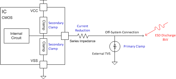
Fig. 100 ESD Protection Network for Off-System Connections
The primary clamp (the external TVS) clamps the electrode voltage to a lower, manageable level. This clamping action reduces the current into the sensitive internal circuit. A series resistance of a few hundred ohms to a few thousand ohms between the TVS and the MCU IO further reduces this current, and is required for the TVS to work properly. The remaining voltage present on the IO is clamped with the on-chip ESD protection clamps.
The TVS diode should be placed close to the electrode where and electrostatic discharge is likely to enter the system, and must have a low impedance path to the circuit return (ground) net.
Design Actions Required
CapTIvate™ Peripheral EMC Features
Internal protection ESD clamps on the IO provide some chip-level protection during device handling and product assembly, but this should not be solely relied on for system level ESD protection.
Hardware Design Principles
Populate a 470-1k ohm resistor in series with the electrode to provide ESD protection, with a protection clamp such as a TVS diode placed between the electrode and ground (return) on the electrode side of the resistor.
Follow recommended hardware best practices for noise immunity
Signal Processing Tools
Debounce of at least one sample is recommended to reduce the possibility of a false detection due to a discharge on an IO during a conversion. ESD transients are fast, and in theory do not affect multiple samples in a periodic way (like RF interference, for example).
Electrical Fast Transient (EFT)
Electrical fast transients are common in industrial environments as well as within commercial products that contain switching inductive loads. These transients are similar in nature to ESD, but exhibit a lower magnitude and longer event length. When high-current inductive loads are switched on and off, high voltage transients may appear on power supply lines. Transients may also appear on signal lines if a system is connected to another system that is generating noise. The transients are a result of the inductance in the load that attempts to maintain the flow of current, and in so doing generates large voltages.
The IEC test simulates these threats by injecting bursts repetitively into the supply or signal lines of a system, in differential or common mode (though common mode is the most typical).
Expectations
High voltage transients are one of the issues that must be considered ahead of time when designing the system. They can wreak havoc on simple analog circuits like the MCU reset circuit. However, with proper design techniques it is possible to realize designs with immunity to 4kV per the IEC 61000-4-4 test specification.
Problem
Fast transients can create effects similar to that of conducted noise, but generally only for brief periods of time as the duration of a transient is often quite short (on the order of 50 nanoseconds). This short burst time often means that not every capacitive touch sample will be affected by a burst. The figure below is data captured from a self capacitance button exposed to 1.5kV EFT bursts that were 50ns each. The 50ns transients were repeated at a 5 kHz burst rate for 15ms. That pattern was then repeated every 300ms, per the IEC test specification. The different effects observed on the electrode can be attributed to the amount of time a sample may have overlapped with a 15ms burst window. There is about a 5% chance of a sample overlapping with a burst, due to the 300ms test period. It is important to note, however, that real world threats will likely not follow this pattern! The IEC test should be used as a tool to understand the implications of EFT on a system- but real world testing in-application is just as if not more valuable.
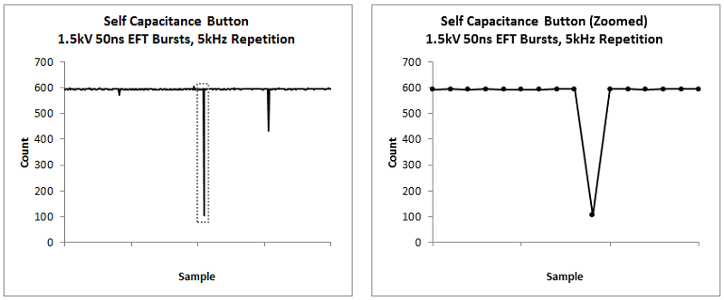
Fig. 101 Self Capacitance Button 1.5kV EFT Test
CapTIvate™ MCU Solution
The primary line of defense against EFT must be hardware design. The best place to stop transients is at the power supply before they have a chance to effect different components of a product. Chances are good that the capacitive sensing MCU will not be the only component that is vulnerable to fast transients. Supplementing a good power supply, software should be EMC hardened. This includes de-bouncing the device reset pin, as well as implementing a watchdog timer. If EFT is a concern in a safety application, memory integrity self-tests should also be applied periodically for robustness.
Heavy debounce of the capacitive touch sensor is also extremely valuable- almost more so than IIR filtering in an EFT environment. Take the figure below as an example. The EFT burst only affected a single sample- something a basic debounce can easily handle. However, the magnitude of the pulse was significant enough to pull down the IIR filter for more than one sample, overwhelming a debounce level of 1 and requiring a debounce level of 2+ or a weaker filter coefficient.
In addition to debounce, applying oversampling improves EFT immunity more than IIR filtering, because of the finite impulse response nature of the averaging filter.
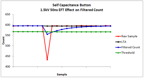
Fig. 102 Self Capacitance Button 1.5kV EFT Test - Filter Ineffectiveness
Design Actions Required
CapTIvate™ Peripheral EMC Features
Integrator-based charge transfer sensing technology
Hardware Design Principles
If possible, design a robust power supply for the system that blocks high frequency transients
Follow the same layout techniques as presented in the RF immunity section
Signal Processing Tools
Re-purpose the reset pin as a non-maskable interrupt (NMI) to debounce potential IC reset conditions.
RF Susceptibility (Conducted and Radiated)
Capacitive touch circuits are inherently vulnerable to RF interference, since it can lead to injected noise currents into transmit (Tx) and receive (Rx) sensing IOs. By applying a combination of peripheral features, hardware techniques, and signal processing, it is possible to realize capacitive touch designs that are robust in the presence of RF interference.
RF interference will be broken down into two categories (conducted and radiated) based upon the frequency of the interference. The distinction between the two is important, as it defines the nature of the coupling medium between the aggressor and the victim. The breakdown is as follows:
Conducted RF Interference
10’s of kHz to 10’s of MHz
Long wavelengths
PCB traces are not efficient antennas
Noise is generally assumed to be coupled into the system via the power supply or through IO cables
Cables are of sufficient length to be efficient antennas
Generally of the most concern for capacitive touch circuits since the frequency range overlaps with the charge transfer frequency range
Radiated RF Interference
100’s of MHz to GHz
Short wavelengths
PCB traces can be efficient antennas
Generally of less concern for capacitive touch circuits
Expectations
The following table breaks down what kind of immunity can be expected when testing a system to the IEC 61000-4-6 specification.
IEC 61000-4-6 Class A Immunity Table (Fully Functional in Presence of Noise)
Sensing Method |
Sensor Type |
Direct Noise Coupling to DC Supply |
Noise Coupling to AC Supply |
|---|---|---|---|
Self |
Buttons |
Level 3 (10V RMS) |
Level 3 (10V RMS) |
Self |
Sliders/Wheels |
Level 3 (10V RMS) |
Level 3 (10V RMS) |
Self |
Proximity |
Level 1 (1V RMS) |
Level 1 (1V RMS) |
Mutual |
Buttons |
Level 2 (3V RMS) |
Level 3 (10V RMS) |
Mutual |
Sliders/Wheels |
Level 1 (1V RMS) |
Level 2 (3V RMS) |
Conducted RF Noise Test System
Conducted noise immunity is most reliably tested with the coupling/decoupling network method as specified in IEC 61000-4-6. A block diagram of the test configuration is shown below. This test setup couples noise directly onto the DC power supply rail to the equipment under test. This is the worst-case coupling location, as no power supply filtering is applied. Most products are not stressed to this level, as some filtering occurs in the AC to DC power supply itself.
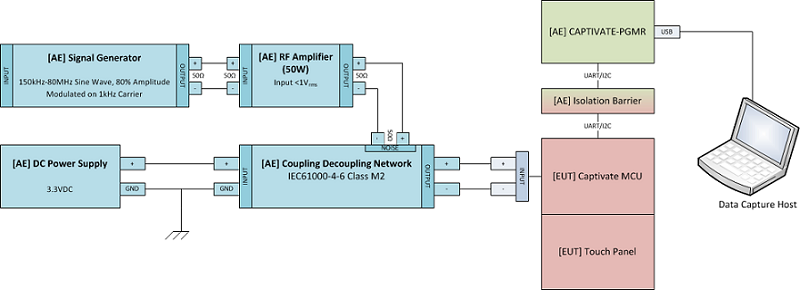
Fig. 103 Conducted RF Test System
The frequency range tested is typically 150 kHz to 80 MHz, amplitude modulated at 80% depth on a 1 kHz carrier frequency to simulate real threats.
Problem
The problem with RF interference is that it leads to injected currents that can couple into receive (Rx) electrodes. Typically, the currents are common mode in nature with respect to some reference (usually earth ground). The adverse effects observed on capacitive touch circuits are different for self capacitance than for mutual capacitance, so the two will be treated separately in the following section.
Self Capacitance
Self capacitance sensors experience several different effects in the presence of noise depending upon the following factors:
Frequency of the noise.
If the noise is centered directly on the conversion frequency or its lower harmonics (+/- 50 kHz), the measurement data will be corrupted positively and negatively, as shown below. This occurs whether or not a touch is present, although the effect is amplified when a touch is present (as shown).
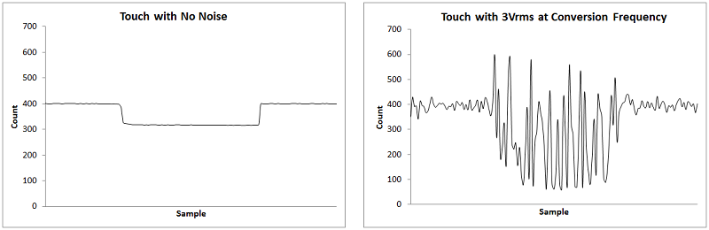
Fig. 104 Self Capacitance Button with No Noise and 3Vrms Conducted Noise at Conversion Frequency
If the noise is nearby the conversion frequency, but not directly aligned with it or a low harmonic, the measurement will not be corrupted but it will experience an increase in sensitivity to touch with a time-varying noise component.
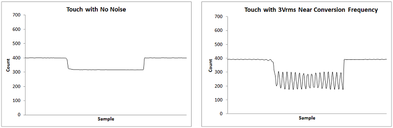
Fig. 105 Self Capacitance Button with No Noise and 3Vrms Conducted Noise nearby the Conversion Frequency
Note that the measurement is stable, and the noise only occurs in one direction. Self capacitance sensors will exhibit susceptibility in this way beginning just below their charge transfer frequency and going out past it with diminishing noise farther out in frequency.
Amplitude of the noise. As the noise amplitude increases, the average delta due to a touch increases. This is a result of injected current into the Rx. This effect shows up as an increase in sensitivity to touch. For example, a button may trigger with a few mm of proximity rather than a full touch.
Mutual Capacitance
Mutual capacitance sensors exhibit corruption of data if noise is present at the conversion frequency or its lower harmonics. The susceptibility band is typically 100 kHz around the conversion frequency. The effect can be seen in the diagram below.
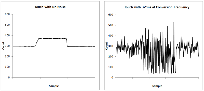
Fig. 106 Mutual Capacitance Button with No Noise and 3Vrms Conducted Noise
Notice how the data captured is completely unusable at this point. If the recommended layout practices are not followed, the result will be a widening of the susceptibility band in frequency beyond the typical value of ~100 kHz. This will limit the performance of the frequency hopping solution described next.
CapTIvate™ MCU Solution
Several methods are employed to improve immunity to conducted and radiated RF interference:
Liberal use of ground structures in the PCB layout to reduce the fringe free-space coupling of the electrode and its trace back to earth ground and the user.
Frequency hopping is applied to prevent noise in a given frequency band from corrupting the measurement by aggregating the data from 4 different conversion frequencies with the multi frequency processing (MFP) algorithm
In mutual mode, filter capacitors are placed between Rx lines and circuit common to narrow the susceptibility band in frequency, improving the benefit of frequency hopping
In self mode, spread spectrum clock modulation and the dynamic threshold adjustment (DTA) algorithm are applied to compensate for the increased sensitivity to touch
Oversampling, IIR filtering and debounce may be used to add additional robustness
Self Capacitance
The figure below shows the noise test result at 3 Vrms noise level with self mode. The results include touched dwell at 2 MHz and touched sweep cross 0.3 MHz to 80 MHz.
The 2 MHz dwell point was chosen because it directly overlaps with the primary, base-conversion frequency of 2 MHz. The left half of the figure below shows two sequential touches and the noise is present in all frequency raw date (F0 to F3). The CapTIvate signal processing algorithm can process the raw data and extract the true results.
The right half of the figure is the touched frequency sweep result which shows that additional sensitivity is present, particularly in the raw data. The data after the CapTIvate signal processing shows that the signal processing removes most of the significant periodic noise in the signal and also help to compensate the additional sensitivity.
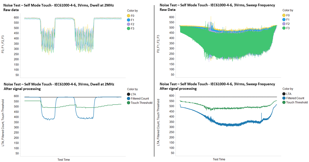
Fig. 107 Self Capacitance Button 3Vrms Conducted Noise
Mutual Capacitance
The figure below shows the noise test result at 3Vrms noise level with mutual mode. The results include touched dwell at 4 MHz and touched sweep cross 0.3 MHz to 80 MHz.
The 4-MHz dwell point was chosen because it directly overlaps with the primary, base-conversion frequency of 4 MHz. The left half of the figure below shows two sequential touches. That noise is present only in the raw data at F0; F1 to F3 are clean. The CapTIvate signal processing algorithm can process the raw data and extract the true results.
The right half of the figure is the touched frequency sweep result which shows that the fundamental conversion frequencies and their harmonics are identifiable in the raw data (F0 to F3). The filtered count after CapTIvate signal processing has minor glitches but they do not affect sensitivity and overall performance.
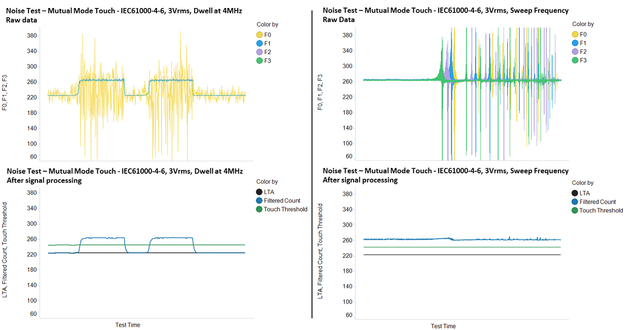
Fig. 108 Mutual Capacitance Button 3Vrms Conducted Noise
Design Actions Required
Designing for immunity to RF interference does require hardware and software considerations. Be sure to review the final section of this guide, Noise Mitigation Steps, for implementation details.
CapTIvate™ Peripheral EMC Features
Integrator-based charge transfer method
Offset subtraction signal chain block
Frequency hopping
Spread-spectrum clocking
Hardware Design Principles
Implement conducted noise immunity layout best practices, taking into account the thickness and dielectric of the overlay material
Eliminate or limit use of off-board connectors that carry capacitive sensing lines
Signal Processing Tools
Noise Mitigation Steps
One of the nice things about designing for EMC is that many of the techniques used to improve a design for one type of noise also tend to improve the design for other types of noise as well. This section steps through noise mitigation steps that should be applied to all designs that require noise immunity. It is best to think of this section as a design check list. All of the items discussed here should be applied when designing a product to have robust noise immunity.
Determine whether the design will be using self or mutual capacitance (or both).
Before beginning a PCB layout, review the hardware checklist.
When configuring a project in the CapTIvate™ Design Center, review the tuning checklist.
Noise Immunity Hardware Check List
Review this check list before starting a PCB layout.
Follow electrode design best practices for noise immunity.
Utilize dense return (ground) plane structures to limit fringe E-field lines.
For mutual (projected) capacitance sensors, populate a 68pF ceramic capacitor between each Rx and circuit return (ground). This capacitor should be placed close to the MCU. It is also a good idea to allow a provision to populate a capacitor between each Tx and circuit return, should it be needed during qualification. The TI noise immunity reference designs do not require the Tx capacitor.
Avoid routing capacitive sensing lines (Rx’s or Tx’s) through board-to-board connectors or cables. Connectors can be significant noise receptors.
Optimize the overlay thickness as much as possible. The thicker the overlay material, the higher the chance of a touch on one key affecting a nearby key. With thinner overlays, electrodes will be more susceptible to ESD. The sweet spot is 1.5mm to 4mm for a typical PC/ABS/acrylic overlay.
Use good power supply design principles to limit noise at the entry point. If possible, implement a common mode choke coil with a high impedance to common-mode noise in the range of 100 kHz to 100 MHz.
Noise Immunity Electrode Design Best Practices
When designing for noise immunity, there are several best practices to apply to electrode geometry. Self capacitance and mutual capacitance will be discussed separately.
Self Capacitance
In the case of self capacitance, 3Vrms immunity is usually attainable without significant overhaul to the electrode design principles discussed in the button design section.
The following principles should be applied:
Limit the size of the electrodes where possible. Do not oversize electrodes beyond what is needed to achieve the desired sensitivity with the overlay that will be used with the product.
Avoid air gaps in the overlay stack up
Keep traces from the MCU to the electrode as short as possible
If possible, do not place electrodes on the edges of the PCB, as this limits the effectiveness of ground shielding
Mutual Capacitance
Mutual capacitance requires a specific geometry to achieve immunity. The layout below depicts the recommended geometry. The goals are as follows:
Limit the size of the Rx
Overlay stack up air gaps are not permitted for mutual capacitance
Optionally, place a small ground fill in the center of the electrode to add a path for noise currents into the ground plane and not into the electrode during a touch
Route all Rx signals on the bottom layer if possible to limit their exposure to a touch
Keep the number of Tx lines per Rx as low as possible. This limits the vulnerability of the receiver to noise.
Fig. 109 Mutual Button Geometry
The recommended mutual capacitance button geometry is as follows:
Parameter |
Value |
|---|---|
Overall Geometry |
10mm x 10mm |
Plane Keepout |
0.5mm from overall geometry on top layer, flooded on bottom layer |
Tx Thickness |
1mm |
Rx Thickness |
0.5mm |
Tx to Rx Spacing |
0.5mm |
This electrode geometry has been proven with overlays up to 3mm of thickness.
For conducted noise immunity considerations and ESD protection, we recommend to consider in the design external component which can be populated if needed.
For mutual (projected) capacitance sensors:
populate a 68pF ceramic capacitor between each RX and circuit ground. (This only applies to Mutual capacitance mode)
Populate a 470 Ohm series resistors on each RX pin
The additional capacitance helps to minimize the effects of EMI and the conducted noise immunity. If DVCC mode is enabled, this capacitor can also help to ensure that the ratio of RX parasitic capacitance (Cp) to RX-TX mutual capacitance (Cm) is within the range that is specified in the data sheet. The additional resistors help to lower the system emissions, improve RF noise immunity and reduce the current flow into the circuit. These are multipurpose series resistors that work with a TPD1E10B06 transient-voltage suppressor (TVS) diode if the system requires Electrostatic Discharge (ESD) protection. Follow also Electrostatic Discharge (ESD)
The additional components should be placed close to the MCU. (The shunt capacitor only applies to Mutual capacitance mode)
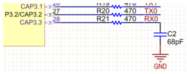
Fig. 110 Mutual Capacitance Shunt Capacitor
Noise Immunity Electrode Shielding Best Practices
Proper ground shielding of electrodes is required to achieve noise immunity. This applies to both self and mutual capacitance designs.
Self Capacitance Shielding
For self capacitance designs, utilize a solid ground or power plane on the top layer of the PCB, and a medium-density hatched power or ground plane on the bottom layer of the PCB. As an example, if the CAPTIVATE-BSWP panel (which was designed for low power battery operation) was modified to attain noise immunity, the following changes would be made:
Removal of the proximity sensor
Addition of a solid ground/power plane on the top layer
Expansion of the hatched ground/power plane on the bottom layer to the size of the PCB
Below are before and after images of the top and bottom layers, applying the principles described above:
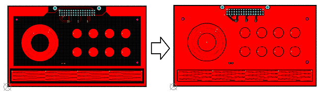
Fig. 111 CAPTIVATE-BSWP Modified for Noise Immunity (Top Layer)
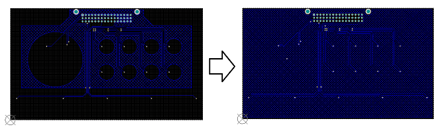
Fig. 112 CAPTIVATE-BSWP Modified for Noise Immunity (Bottom Layer)
The addition of these dense ground structures serves to limit fringing E-field lines as much as possible, stabilizing the electrodes. Normally the addition of this much parasitic capacitance is considered bad practice, but in the case of noise immunity the trade-off is extremely beneficial. In addition, the gain and offset subtraction capability of the CapTIvate™ technology makes it possible to maintain decent sensitivity even with the ground shield structures.
Mutual Capacitance Shielding
For mutual capacitance designs, utilize solid ground or power planes on the top and bottom layer of the PCB. Mutual receive electrodes (Rx’s) are extremely sensitive (on the order of <1mV). As a result, they are very vulnerable to noise currents. It is necessary to keep the Rx tracks as short as possible and as well-shielded as possible.
Tuning Check List
Review this check list when tuning a design that requires noise immunity.
If RF immunity is required, enable noise immunity mode in the CapTIvate™ Design Center. Controller Properties -> Noise Immunity-> Enable Noise Immunity
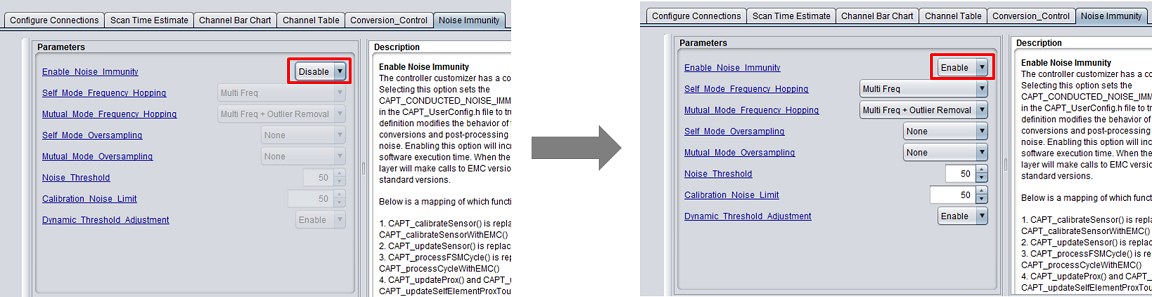
Fig. 113 Step1
By enabling noise immunity feature, you will enable the Frequency Hopping and you can also select the level of oversampling feature if needed. Controller Properties -> Noise Immunity-> Self Mode Oversampling, Mutual Mode Oversampling
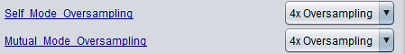
Fig. 114 Step2
If you it is a Second-Generation device, you should also enable the DVCC Charge Mode and the Input Impedance Bias Current. Controller Properties -> Noise Immunity-> DVCC Charge Enable, Input Impedance Bias Current
Fig. 115 Step3
For mutual (projected) capacitance sensors, use a conversion frequency of 2 MHz to 4 MHz. If the phase lengths are both set to 1, a frequency divider of f/4 provides an effective conversion frequency of 2 MHz. Utilizing a faster conversion frequency increases the effectiveness of the frequency hopping mechanism by providing a wider spread between hop points. Sensor Properties -> Conversion_Control -> Frequency Divider
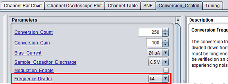
Fig. 116 Step4
For self capacitance sensors, enable modulation. In self mode, the modulation spread the conversion clock frequency and reducing noise spikes directly at the conversion frequencies and lower harmonics. For mutual (projected) capacitance sensors, disable modulation. In mutual mode, the modulation interferes with frequency hopping, as it widens the susceptibility bands. Sensor Properties -> Conversion_Control -> Modulation Enable
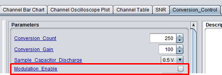
Fig. 117 Step5
Set strong debounce settings. A value of 2 or greater is recommended. Sensor Properties -> Tunning -> Debounce Threshold
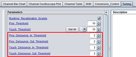
Fig. 118 Step6
Set a strong count filter beta. A value of 2-3 for buttons and 1-2 for sliders/wheels is recommended. Sensor Properties -> Tunning -> Count Filter
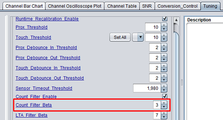
Fig. 119 Step7
Set an error threshold for each sensor. For mutual capacitance, a good rule-of-thumb is to take the conversion count + 2-3x the maximum expected touch strength. For example, if a button has conversion count setting of 400, and a maximum expected delta due to touch of 100, than setting an error threshold of 600-700 would be appropriate. This serves to “cap” every conversion result to a maximum value. If noise in the system attempts to cause a conversion to continue beyond the error threshold, then the conversion will be halted. This prevents rogue samples from having extremely long sample times and effecting the response time / filtering of the system. For self capacitance, a good value is the conversion count x 1.25. For example, a sensor with a conversion count of 800 would have an error threshold of 1000. Sensor Properties -> Tunning -> Error Threshold
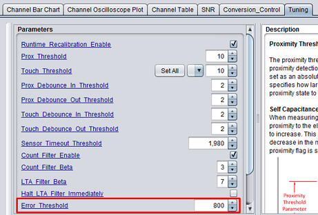
Fig. 120 Step8
After making the change to these configurations. Don’t forget to generate the new project with the new configurations or update the existing project and program the device with new project. Controller Properties -> Generate Source Code
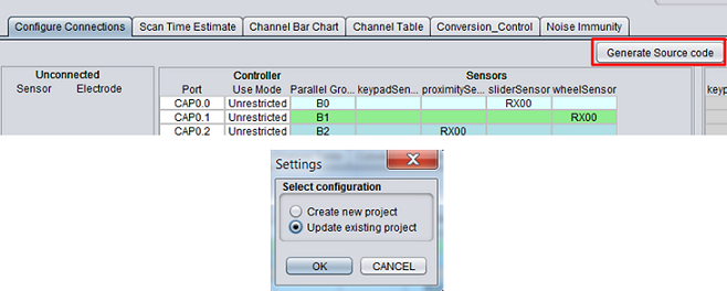
Fig. 121 Step9
Temperature Drift
For the outdoor applications, depending on the geographical region and the season, the ambient temperature can vary and drift over time. CapTIvate technology provides build in Long Term Average tracking and Auto Runtime Recalibration algorithm to ensure that each element is within the resolution and sensitivity band that was specified.
Temperature Drift Impact on Conversion Results
A temperature characterization test was performed on self and mutual mode sensors with both first-generation and second-generation devices from -40 °C to 85 °C.
Self Mode:
Test Setup:
Hardware Used |
Software Configuration |
|---|---|
CAPTIVATE-BSWP |
Conversion Count: 500 (Calibrated at room temperature) |
CAPTIVATE-FR2633 |
Conversion Gain: 100 |
CAPTIVATE-FR2676 |
Frequency Divider: f/2 |
CAPTIVATE-PGMR |
DVCC Mode (2nd Gen): Enabled |
Input Impedance Bias Current(2nd Gen): Enabled |
Test Results:
The device under test is calibrated at room temperature and the conversion result was captured at different temperature points.
Device Generation |
Conversion Results Drift |
|---|---|
1st Gen |
-2.6 counts/°C |
2nd Gen |
-1.4 counts/°C |
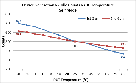
Fig. 122 Self Mode Temperature Drift
Mutual Mode:
Test Setup:
Hardware Used |
Software Configuration |
|---|---|
CAPTIVATE-PHONE |
Conversion Count: 250 (Calibrated at room temperature) |
CAPTIVATE-FR2633 |
Conversion Gain: 100 |
CAPTIVATE-FR2676 |
Frequency Divider: f/2 |
CAPTIVATE-PGMR |
DVCC Mode (2nd Gen): Enabled |
Input Impedance Bias Current (2nd Gen): Enabled |
Test Results:
The device under test is calibrated at room temperature and the conversion result was captured at different temperature points.
Device Generation |
Conversion Results Drift |
|---|---|
1st Gen |
-0.2 counts/°C |
2nd Gen |
-0.1 counts/°C |
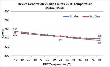
Fig. 123 Mutual Mode Temperature Drift