
|
CapTIvate™ Technology Guide
v1.10.00.00
|
|
CapTIvate™ Technology Guide
v1.10.00.00
|
Capacitive touch detection is sometimes considered more art than science. This often results in multiple design iterations before the optimum performance is achieved. There are, however, good design practices for circuit layout and principles of materials that need to be understood to keep the number of iterations to a minimum.
Good sensor design is the foundation for a successful touch product.
The purpose of this design guide is to provide guidance for the design and layout of capacitive touch sensors so that they can achieve maximum performance. By achieving maximum performance in the hardware, the CapTIvate™ capacitive touch software library can perform the capacitive touch measurements consuming the lowest power. Tuning guides, along with the CapTIvate™ Design Center are used to help tune the performance of the capacitive touch application.
Starting any new capacitive touch design can be a challenging task. This section will guide you through this process and help determine what is important for your design and end application.
Identify Sensors
First we want to identify the types of sensors that you are considering for your application and provide some basic design guidelines.
Identify Care Abouts
Next it is important to identify any special requirements for the end application, such as low-power, noise immunity, moisture, etc.
Creating a reliable capacitive touch design can be a time consuming process that starts with designing sensors, laying out a PCB, writing lots of code and finally performing an iterative sensor tuning process to achieve the desired performance. The CapTIvate™ Technology sensor design process accelerates the capacitive touch development cycle through automation, helping get your product to market faster.
Creating a new sensor design
We begin the process by creating a new capacitive touch design using the CapTIvate™ Design Center. With a few simple drag-n-drop inputs and configuration selections, the CapTIvate™ Design Center will automatically determine the optimal pin assignments between the target MCU and the sensors (CapTIvate™ Technology peripheral can measure four channels in parallel). Alternatively, connections can be manually assigned or reserved for those applications with specific routing requirements.
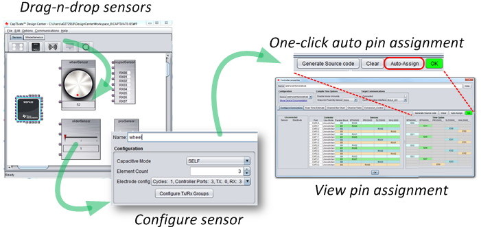
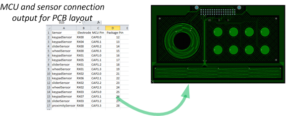
Layout PCB
Once the pin assignments have been made, the MCU pin to sensor electrode connection information is exported to a .csv file and can be used during the PCB layout and design.
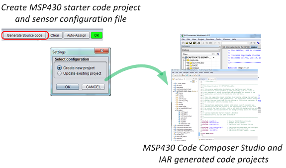
Generate configuration and starter project files
Now we are ready to create a custom starter code project based on our sensor design. The CapTIvate™ Design Center creates a fully working capacitive touch application that can be imported into Texas Instruments Code Composer Studio (CCS) or IAR Embedded Workbench. In addition to the application, the CapTIvate™ Software Library and MSP430 driver-lib are automatically included with the project, as portions of the libraries are needed during the development cycle.
Program target MCU
Import the generated CapTIvate™ project into Code Composer Studio or IAR IDE, compile and program the target MCU. The specific steps to perform the programming operation depend on the IDE, however, once the target MCU is programed, you are ready to start running your first capacitive touch application without having to write a single line of code!
Didn't get it right the first time? Changes to a sensor design is simple. We use the CapTIvate™ Design Center to modify our sensor design project, then generate an updated configuration file. Simply copy the new configuration file and replace the existing one in the CCS or IAR application project and rebuild the application. That's it!
Tune Sensors Our PCB is ready to go so we can now begin the process of tuning the sensors for the desired touch and feel. With the MCU programmed with our application and running, the sensors are scanned and real-time data is transmitted to the CapTIvate™ Design Center using the high-speed HID serial bridge MCU on the CAPTIVATE-PGMR PCB. The CapTIvate™ Design Center has several different views to display and monitor the sensor response and allow quick modifications in real-time to the sensor's parameters, providing instant feedback.
Generate final configuration Once our desired touch and feel is achieved, the final sensor configuration can be generated, then programmed into the target MCU. That's it! Using the steps outlined above, capacitive sensor design time can be dramatically reduced.
Congratulations! You are done with your design and ready to go to market.
In this section we will cover both mechanical as well as common layout practices.
Capacitive touch detection is a type of analog-to-digital converter (ADC), specifically a capacitance-to- digital converter. As with most ADCs, the terms of interest are resolution, signal-to-noise ratio (SNR), and linearity, in the specific cases of wheels and sliders. Throughout this document, the design guidance helps to maximize signal, minimize noise, and address when these two goals are at odds.
As mentioned above, the basis of capacitive touch detection is the ability to measure a change in capacitance. This change in capacitance is the signal that the capacitive touch solution identifies. The term sensitivity is often used to describe the signal strength a more sensitive solution has a stronger signal.
Sensitivity is measured in capacitance per counts. In the context of capacitive touch detection, the magnitude of change introduced by a touch is on the order of picofarads or hundreds of femtofarads. It is not uncommon for a solution to see a touch introduce 1 pF of change and be measured as 300 counts. And while the sensitivity might be 3.3 fF/count, this should not be considered until the noise is factored in. Refer to the section on Noise below.
Sensitivity can be controlled within firmware, but the goal is to provide good sensitivity with the hardware, so that the lowest sensitivity settings can be used in firmware, which provides the lowest-power solution. Referring to the Equivalent circuit for a self capacitive sensor, C_touch must be maximized, while the other four capacitances must be minimized. The capacitances of the trace and electrode are approximated as parallel plate capacitances. The following equation serves as the basis for layout recommendations.
C = Er x E0 x A/d (1)
The dielectric constant (Er), area (A), and distance (d) are described throughout this document with the intent of positively influencing the capacitance for a touch system.
Although parasitic capacitance is presented separately, it is a part of the sensitivity and signal. As already mentioned, the capacitance of interest is the relative change in capacitance. The change in capacitance is based upon the touch interaction, but this change is perceived relative to the parasitic capacitance of the system. The parasitic capacitance is also called the steady-state capacitance or baseline capacitance. If the introduced change is 100 fF, then the sensitivity, which is the relative change in capacitance, can be increased by decreasing the parasitic capacitance.
The capacitances C_trace, C_electrode, and C_parasitics are generically referred to as parasitic capacitance.
The mechanicals are the mechanical characteristics of the design. The mechanicals include the overlay material, ink on top of the overlay, any adhesives used to bond the electrode to the overlay or enclosure, and any transition materials used to remove air gaps between the electrode and the overlay. Mechanicals also include the types of materials used for the electrodes. The mechanicals affect both the signal and the parasitic capacitance.
The goal of this section is threefold:
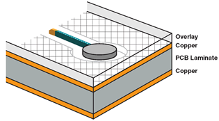
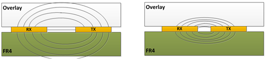
The following figure shows a typical stackup for a capacitive touch solution. One of the main goals of this stackup is to reduce (or eliminate, if possible) any low-dielectric (air) gaps between the electrode and the area where the touch takes place. The capacitance associated with the stackup has a very strong effect on the signal (change in capacitance from a touch). The signal is directly proportional to the dielectric of the materials. If possible, high-dielectric materials should be used, but at a minimum the stackup should eliminate any air gaps.
Another critical attribute of the stackup is that it should be non-conductive. This is not usually a problem with the overlay material but can be overlooked when choosing adhesives, labels, or inks. Popular adhesives for capacitive touch solutions include 200MP products from 3M™ such as 467MP and 468MP.
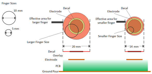
The capacitance of the stackup is a superposition of all of the material, but the overlay is often the dominant material. The type and dimension of the overlay material that is used is determined by the desired aesthetic and from the required amount of protection. A common requirement is rugged (scratch or puncture resistant) and yet lightweight.
The following figure shows the relationship between the thickness of the overlay and the sensitivity of the circuit. From the parallel plate capacitance equation, the capacitance in inversely proportional to the material thickness (C ~ 1/d).
The thickness and dielectric of the material influence the electrode design. The electrode area is a function of the area of interaction (a fingertip or the palm of the hand) while the spacing (to adjacent electrodes or ground fill) is related to the thickness of the overlay. For example, with a 2-mm overlay that has a dielectric of 3, the spacing should be approximately 1 mm (half of the thickness). Using a higher dielectric material (for example, Er = 6) the thickness could be doubled while maintaining the same level of performance. The following table shows dielectric values for various materials used as overlays.
Table: Material Dielectric and Breakdown Voltage
| Material | Dielectric Constant (Er) (1) | Breakdown Voltage (V/mm) |
|---|---|---|
| Air | 1.0 | 3300 (STP) |
| FR-4 | 4.8 | 20000 |
| Glass | 7.6 to 8.0 | 7900 |
| Gorilla® Glass | 7.2 to 7.6 | See Manufacturer (2) |
| Polycarbonate | 2.9 to 3.0 | 16000 |
| Acrylic | 2.8 | 13000 |
| ABS | 2.4 to 4.1 | 16000 |
(1) Relative permittivity
(2) http://www.corninggorillaglass.com
The table above also includes the breakdown voltage for different overlay materials. This should be considered when designed for ESD protection. ESD solutions should be system solutions, and any additional components should complement the protection provided by the overlay.
The performance is affected by the conductive materials that are used for the electrode and for the trace between the electrode and the microcontroller. Most applications use copper on a PCB, and copper has a resistivity of 1.7x10⁻⁶ Ohm-cm (3). As the resistivity of the conductor increases, the ability to move charge to and from the electrode decreases. This has the same effect as an increase in parasitic capacitance. This increase in resistivity, like an increase in parasitic capacitance, reduces the system sensitivity. The table below shows the resistivity for materials that are commonly used in touch applications.
(3) Resistivity is given in Ohm-cm so that resistance is equal to the resistivity times the length divided by the cross-sectional area : R = p x L / A.
Table: Resistivity of Materials
| Material | Resistivity, p (Ohm-cm) |
|---|---|
| Copper | 1.68x10⁻⁶ |
| Silver | 1.59x10⁻⁶ |
| Tin | 1.09x10⁻⁵ |
| Indium Tin Oxide | 1.05x10⁻³ (1) |
(1) This resistivity is for a film thickness of 270 nm. Typically, vendors provide sheet resistance instead of resistivity for ITO, which is on the order of 10 to 100 Ohms per square.
When using high-resistivity materials, generally the recommendation is to increase the area of traces to reduce the resistance (at the cost of capacitance). ITO solutions provide lower sensitivity, which must be compensated for in the capacitance measurement algorithm by longer measurement times.
Not all applications fit into the typical category, and this section describes two special cases. The first is intentional air gaps that are greater than 2 mm between the electrode and the overlay material, and the second is the use of gloves.
In some applications, components are on the same layer as the electrode. This prevents the overlay from being directly applied to the electrode. A common example of this is when an LCD is mounted near the electrode (see diagram below). Another scenario is when the overlay material is not a uniform surface and, therefore, the electrode cannot make direct contact with the overlay.
In either case, the gap must be filled or bridged with a non-conductive filler (typically adhesive) or a conductive extension. When the gap is in excess of 2 mm, then a conductive extension, either foam or metal, should be used. The metal or foam must be malleable to conform to the shape of the surfaces and prevent the formation of gaps. As shown in the Figure above, the area created by the foam or metal in contact with the overlay is now the area that influences the capacitance.
Gloves are simply another layer of medium between the electrode and the finger, and the same principles of thickness and dielectric apply. The challenges with glove applications include the ability to support both gloved and ungloved hands as well as the variation in the types of gloves the application might require. Typical leather or plastic gloves have a dielectric constant in the range of 2 to 4, and fabric gloves and gloves with insulation can have a dielectric constant less than 2.
After the mechanicals are understood, the electrodes can be sized and designed to provide the most signal. Independent of the mechanicals, the layout design is affected by the distance between the microcontroller and the electrodes, the PCB stackup (for example, one layer, two layer, or four layer), and other electrical circuits on the PCB.
The first item to consider relates to the schematic and the placement of any external components that are associated with the capacitive touch solution. A typical example is ESD protection components such as a series current limiting resistor. In all cases, the components should be kept as close as possible to the microcontroller. As the components move farther away from the microcontroller, the increased area correlates to an increased risk of noise or ESD conducting into the device.
The parasitic capacitance of the trace comprises several major and minor capacitance contributors. For simplicity, C_trace represents the major capacitances formed between the trace line and the ground pour on the bottom side and surrounding it. The top and cross-sectional views of a typical two layer PCB are shown in Figure 6. The capacitance, C_trace, is determined by the trace line width (W), dielectric thickness (H), trace thickness (T), and the relative permittivity of the PCB material (Er).
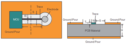
The capacitance per unit length of the trace is an important concept to emphasize the need for short traces. Increasing the distance of the trace increases the parasitic capacitance associated with the trace. Increasing the trace length can also increase susceptibility to noise. Therefore, the trace routing between the microcontroller and the electrode should be kept as short as possible. This is not always possible, so it is important to understand the increase in parasitic capacitance associated with the trace routing.
The capacitance per unit length should be kept as small as possible to minimize the parasitic capacitance (C_trace) and ultimately maximize sensitivity. As previously mentioned, the dominant capacitance in C_trace is the parallel plate capacitance between the trace and the surrounding ground pour. The ability to reduce this capacitance is a direct function of the PCB manufacturing capabilities. Tighter tolerances and smaller minimum dimensions (trace width and separation) allow for thinner traces and larger separation, which result in lower capacitance per unit length. These manufacturing capabilities typically come at a higher cost.
The table below shows how the capacitance per unit length changes with the variation of different dimensions. These values are taken from Reference Section in the Coplanar Waveguide Analysis/Synthesis Calculators.
Table: Calculating Results of Capacitance per Unit Length
| W (mm) | S (mm) | T (mm) | H (mm) | Er | C (pF/cm) |
|---|---|---|---|---|---|
| 0.152 | 0.152 | 0.036 | 1.6 | 4.6 | 0.633 |
| 0.152 | 0.254 | 0.036 | 1.6 | 4.6 | 0.555 |
| 0.152 | 0.381 | 0.036 | 1.6 | 4.6 | 0.496 |
| 0.203 | 0.152 | 0.036 | 1.6 | 4.6 | 0.692 |
| 0.203 | 0.254 | 0.036 | 1.6 | 4.6 | 0.602 |
| 0.203 | 0.381 | 0.036 | 1.6 | 4.6 | 0.543 |
| 0.254 | 0.152 | 0.036 | 1.6 | 4.6 | 0.740 |
| 0.254 | 0.254 | 0.036 | 1.6 | 4.6 | 0.641 |
| 0.254 | 0.381 | 0.036 | 1.6 | 4.6 | 0.578 |
| 0.254 | 0.152 | 0.036 | 2.54 | 4.6 | 0.736 |
| 0.254 | 0.254 | 0.036 | 2.54 | 4.6 | 0.637 |
| 0.254 | 0.381 | 0.036 | 2.54 | 4.6 | 0.566 |
The table above shows that increasing the space, S, between the trace line and the ground is an effective way to reduce the parasitic capacitance. However, increasing the separation can have negative effects that need to be understood. One effect is simply increased board space. Increasing the dimensions can lead to larger PCBs and higher cost. Another effect is related to noise. The larger separation makes traces more sensitive to touch events (touching the trace instead of the electrode) and more susceptible to radiated emissions.
In practice, the designer should choose a balanced S value, and a value of 1/8 of the overlay thickness is typically acceptable. Additionally, a hatched ground is commonly used instead of solid fill near the trace lines to reduce the area and consequently the parasitic capacitance.
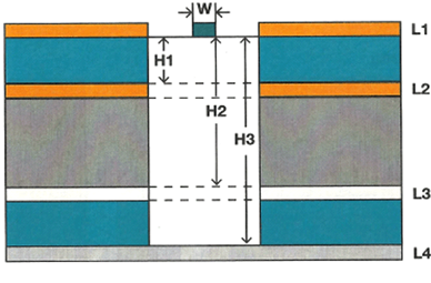
The table above also shows that as H gets smaller, the parasitic capacitance increases, which results in a decrease in sensitivity. In most applications, a two-layer PCB is used, and a standard FR4 PCB with the thickness of 1 mm to 1.6 mm is recommended. If a multilayer board is used, it is recommended to keep the H as large as possible. With complex multilayer boards (more than six layers), it is important to recognize that the absence of copper in the internal layers can cause issues and the height, H, between the top layer and the bottom may be smaller than predicted.
The figure below shows an example of a four-layer PCB, which may be desired in applications with limited board space. To reduce parasitic capacitance, the ground pour is usually placed on the lowest layer underneath the trace to provide the largest H. If it is difficult to achieve the maximum height, then a narrower W, a larger S, or even a hatched ground fill are alternatives to reducing the parasitic capacitance.
To determine the maximum trace length from the capacitance per unit length, some additional information is needed. The following example is used to calculate the maximum distance for a trace with a capacitance per unit length of 0.58 pF/cm. The capacitance introduced by a touch, C_touch, is assumed to be approximately 1 pF. To make sure that the capacitance induced by a finger is large relative to the parasitic capacitance, the total parasitic capacitance (C_parasitics, C_trace, and C_electrode) should be in the range of 10 pF to 20 pF (the change is at least a 5% change). Assuming that the C_electrode is approximately 3 pF, the C_parasitics is 5 pF, and the capacitance per unit length is 0.58 pF/cm, so the trace line length L should be no longer than 210 mm. If the electrode is larger (for a proximity application), the capacitance itself is larger (assume approximately 8 pF for this example), so the maximum trace line length L is reduced to 120 mm.
Generally speaking, the trace width W should be as thin as the PCB technology allows, because a short and narrow trace line is preferred. The trace thickness T and the relative permittivity of the material Er also have significant influence on capacitance per unit length, but they are determined by PCB manufacture process and are usually difficult to change.
Some designs require the electrode to be off-board, and consequently a connector is used to transition the trace from the PCB to a cable or to another PCB. Connectors are generally not desired because like any component there is an associated parasitic capacitance with connector PCB footprint and structure.
In terms of parasitic capacitance and sensitivity, the connector is treated as a parasitic capacitance reducing the sensitivity of the solution. Because the connector is treated as a lumped capacitance, the placement is irrelevant to the sensitivity. However, the placement is important with respect to noise.
The figure below shows that if the aggressor (noise source, N1) is located on the PCB, then the preferred placement of the connector is near the MSP430 microcontroller. The parasitic capacitance associated with the connector shunts high-frequency noise (Z 1/jwC) and increases the noise immunity of the circuit. Conversely, if the aggressor is located off-board (noise source, N2), then the connector should be placed farther from the microcontroller and closer to the electrode. This arrangement minimizes the off-board trace and cable length (which acts like an antenna). When multiple aggressors exist as is shown in the figure below, it is recommended to reduce the effect of the radiators that most closely match the operating frequency of the touch detection circuit.
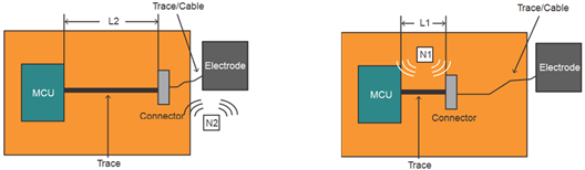
When deciding the position of the connector, the designer must balance the length of the trace and the cable while considering parameters like the background noise.
The routing is typically done with copper, but other materials like silver and ITO can be used. Silver is similar to copper and similar performance can be expected (if the thickness of the materials are also equivalent). ITO is very different from copper, and the difference in resistivity degrades the sensitivity of the solution. Lowering the impedance of the trace (by increasing the width) should be a high priority in the design, even though this comes at the cost of increased parasitic capacitance and reduced noise immunity. Ultimately, the use of materials like ITO requires more processing by the MSP430 microcontroller to adjust to lower sensitivity and increased noise.
As discussed in the Routing section, conductivity becomes an issue in more resistive materials like ITO. Although the transparency of ITO is very good, the resistivity is high when compared to materials like silver and copper. Typically the physical dimensions prohibit increasing the area of the ITO electrodes, and therefore any degradation in sensitivity must be compensated for in the firmware. This typically results in slightly longer measurement times and consequently increased power consumption.
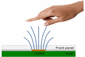
The electrode design must accomplish two goals. First, the design must provide sufficient signal (change in capacitance with interaction). The design must project the e-field up and out so that the appropriate level of sensitivity is achieved at the desired distance. Understanding the stackup, thickness and dielectric, the electrode can be sized and shaped to provide the maximum signal. Second, the electrode design needs to have a minimal parasitic capacitance.
In the following sections the shape and area of the electrode are discussed with the intent of maximizing the signal for different implementations (buttons, sliders, and wheels). The basis for controlling the parasitic capacitance is common to different sensor implementations and is discussed here.
The figure below shows an example PCB cross-section and the important parameters that influence the parasitic capacitance. The height, width, and separation have a direct effect on the parasitic capacitance of the electrode, C_electrode. The fundamental parameter area is not shown in the figure below because this has a direct effect on both the touch capacitance (C_touch) and the parasitic capacitance (C_electrode). This section describes how changes to the height and separation can minimize the parasitic capacitance. The following sections describe how changes to the area can maximize C_touch.
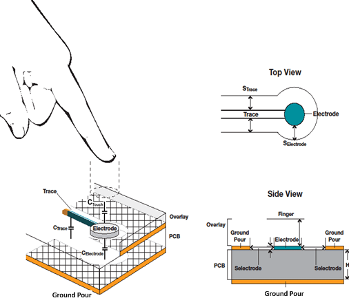
The separation (S_electrode) is directly related to the height of the overlay as described in the Mechanical section. The height is a function of the PCB and is not a parameter that can be easily controlled. The separation is typically the parameter with the most flexibility.
Table: Baseline Electrode Capacitance
| Area(mm2) | Height(mm) | Description | Separation(mm) | Capacitance(pF) |
|---|---|---|---|---|
| 10x10, FR-4 (Er = 4.4) | 1.572 | 2 Layer PCB, L2 | 0.508 | 3.3 |
| 10x10, FR-4 (Er = 4.4) | 1.572 | 2 Layer PCB, L2 | 1.02 | 3.2 |
| 10x10, FR-4 (Er = 4.4) | 1.572 | 2 Layer PCB, L2 | 1.52 | 3.1 |
| 10x10, FR-4 (Er = 4.4) | 1.30 | 4 Layer PCB, L2 | 0.508 | 3.8 |
| 10x10, FR-4 (Er = 4.4) | 1.57 | 4 Layer PCB, L3 | 0.508 | 3.3 |
The table above shows that increasing the height (the distance between the electrode and the reference plane) decreases the capacitance. By decreasing the parasitic capacitance, the relative change in capacitance caused by a touch event is increased. For example, if the change in capacitance associated with a touch is 0.5 pF, the relative change is greater when the base capacitance is 11 pF instead of 12 pF, (5.5% instead of 4.2%).
By default, the CapTIvate™ Software Library drives non-actively scanned electrodes to ground allowing neighboring electrodes to be treated as an extension of the ground pour. Therefore, the spacing between the electrodes follows the same rules for spacing from ground. The goal is provide enough spacing so that the e-field propagates up and through the overlay material. A minimum spacing of one-half the laminate thickness has been found to provide sufficient signal (sensitivity).
The capacitance of the electrode is a function of area, but the shape is important to consider, because the shape can influence the area. An important detail of designing the electrode shape is not to design shapes that have low surface area. The area of each electrode must provide the maximum C_touch, which in turn produces the most signal (the change in capacitance) when a touch event occurs.
In the Connectors section above, the aggressor is assumed to be a point source of noise. In this section, the aggressors are different signals that are routed in close proximity to the capacitive touch sensor trace. These aggressors can be another capacitance sensor trace or non-capacitance sensor lines. Examples of non-capacitance sensor lines include digital signals, analog signals, and high-current signals used to drive LEDs.
Capacitive sensor traces influence neighboring capacitive touch sensor traces. The space between capacitance sensor trace lines, Scs, should be kept as a safe distance (see figure below).
Digital signals are typically PWM signals or communications like I2C or SPI. Unlike the capacitive traces, these signals can act as aggressors and can be active during a capacitance measurement. It is recommended to keep these types of signals at least 4 mm away from the capacitive touch trace. If the digital signal and the capacitive touch trace must cross, then it is recommended to keep the crossing at a 90 degree angle.
Signals used to drive LEDs (unless the LEDs require high-strength drivers) are similar to other digital signals. Therefore, as with digital signals, a distance of at least 4 mm is strongly recommended for S_LED, as shown in the figure below.
As a general rule, LEDs should be driven and the use of high-impedance states should not be used to control the LED. The use of a high impedance to prevent an LED from conducting can result in a significant difference between the on-state and off-state capacitances. This change in capacitance may be detected by the touch solution and treated as a change in the system capacitance, or even worse as a false detection. If the use of high-impedance control of the LED is unavoidable, a discrete capacitor (typically 1 nF is acceptable) in parallel with the LED is recommended.
LED BackLighting can be done easily using a back lighting LED on the opposite side of the PCB
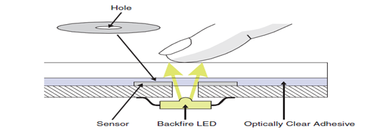
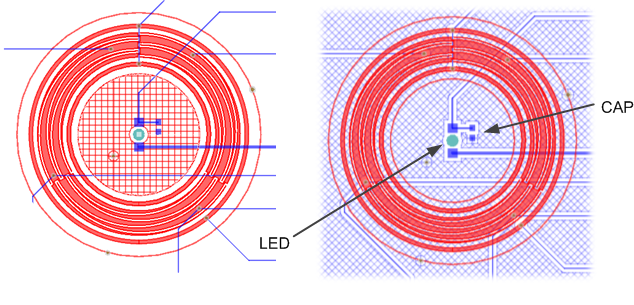
As an example of an LED backlighting technique, the following wheel design has an LED mounted on the backside of the PCB and illuminates through a small hole. In parallel to the LED, a small 1nF capacitor is used to reject changes in capacitance when the LED is switched between ground and high-Z. Also note the hatched ground on both the top and bottom layers to help with noise immunity.
Surrounding ground planes affect the sensitivity of the electrode. This is seen primarily as an increase in base capacitance as the separation from the ground decreases and the area of the ground pour increases. This section looks at the placement of surrounding ground pours and the fill (percent hatch) of those pours.
Planes and pours near the electrode and trace must be connected to a potential and cannot be left floating or in a high impedance state. Such structures serve as a mechanism for noise coupling and are strongly discouraged.
Ground planes, both coplanar and on neighboring PCB layers, reduce noise. This is the same principle discussed in the Routing section. The ground or guard structures are placed as close as possible to reduce noise but also kept far enough away to minimize parasitic capacitance. This separation is a function of the thickness of the materials (overlay, adhesive, etc.) on top of the trace. As mentioned in the Routing section, a good rule is one-eighth the thickness for separation between traces and ground. The separation between electrodes and ground should be at least one-half the thickness.
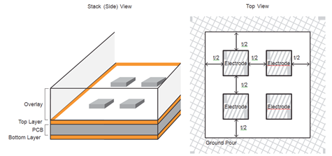
As shown in the figure above, the separation between the electrode and the coplanar ground pour should be at least one half the thickness of the overlay material. Any unused electrode should be held at a logic low level (Vss potential) and not allowed to float. In this way the spacing between electrodes is the same as the ground and electrode distance.
The use of a hatched pour instead of a solid ground pour is a good design practice. This reduces the area and consequently the parasitic capacitance associated with both C_trace and C_electrode. Typically, a 25% fill hatch is sufficient, but this percentage can be increased or decreased to improve noise immunity or sensitivity, respectively.
When designing a button, slider or wheel of any size or shape, a flexible method to control the distance between any sensor and the ground pour is to provide a poly cut-out region around the sensor as shown below.
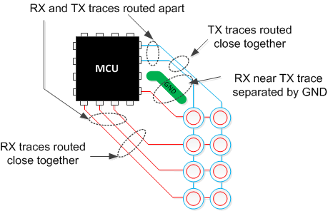
Routing mutual capacitive traces has special considerations compared to self capacitive traces. Specifically, the TX and RX signals on the same layer should be close only in those areas where coupling through a finger touch is expected by design, such as the case with button, slider or wheel elements (electrodes). Anywhere else that TX and RX traces on the same layer are routed close can be susceptible to a "ghost" touch should a finger touch in that area.
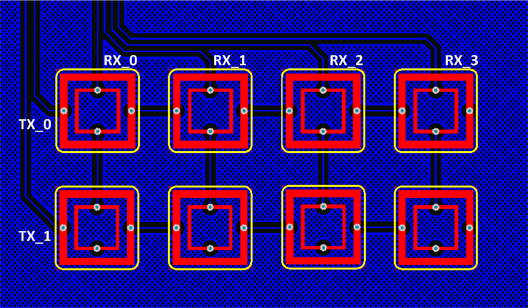
The diagram below shows an 8-button keypad using (2) TX and (4) RX traces. In this layout the TX and RX traces are on the same layer. The TX traces are routed close to each other as are the RX traces. The TX traces are routed away from the RX traces. In this example there is one RX that must be routed near a TX trace. A ground trace/fill is used to separate the RX an TX traces.
A self capacitive button sensor is a single electrode. Self capacitive buttons are simple to layout and each button is assigned to only one pin on the MCU. Self capacitive buttons will provide greater sensitivity as compared to a mutual capacitive button, but are more influenced by parasitic capacitances to ground.
| Parameter | Guidance |
|---|---|
| Radiation Pattern | Between Electrode and Ground |
| Size | Equivalent to interation |
| Shape | Various: typically round or square |
| Spacing | 0.5 x Overlay minimum thickness |
The electrode shape is typically rectangular or round with common sizes of 10mm and 12mm. Ultimately, the size will depend on the required touch area. A good design practice is to keep the size of the button as small as possible, which minimizes the capacitance and will help with the following:
In the diagram below, an example silkscreen button outline pattern is shown.
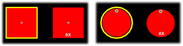
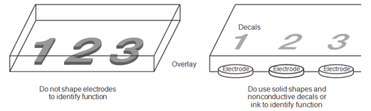
One common mistake is to make the electrode the same shape as the icons printed (in nonconductive ink) on the overlay. As shown in the figure below, this can lead to electrodes with odd shapes that create discontinuities and reduce surface area.
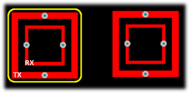
A mutual or "projected" capacitive button sensor requires two electrodes, one as a TX and the other for RX. Mutual capacitive buttons are not as sensitive as self capacitive buttons, however, it is possible to pack the electrodes closer together with a low risk of cross talk between neighboring electrodes. With mutual capacitive electrodes, multi-touch is possible by multiplexing the channels. Multiplexing creates up to 64 electrode pairs or "buttons" that can be scanned using only 16 CapTIvate™ I/O pins.
| Parameter | Guidance |
|---|---|
| Radiation Pattern | Between TX and RX and ground |
| Size | Equivalent to interation |
| Shape | Various: recommend square or shape with corners |
| Spacing | 0.5 x Overlay minimum |
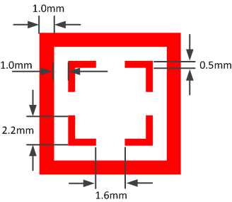
The electrode shape is typically rectangular with common sizes being 10mm and smaller. Ultimately, the size will depend on the required touch area. In the diagram below, the TX and RX electrodes are identified and a suggested silkscreen button outline pattern is shown. The position of the vias on the TX and RX electrodes provide flexible signal connection points when routing traces.
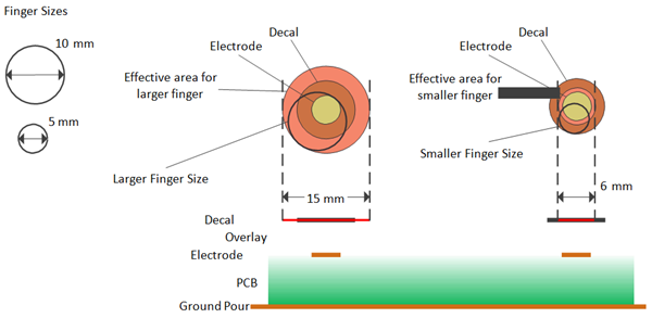
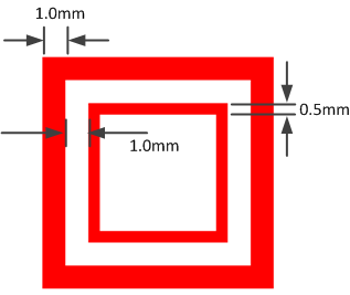
The dimensions shown on a 10mm x 10mm example button are suitable for overlay thickness up to 2mm.
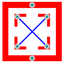
An alternative button design, which can provide better sensitivity and is slightly more difficult to create, forces the e-field lines to be concentrated in the four RX corners.
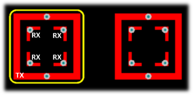
The dimensions shown for this 10mm x 10mm example button are suitable for overlay thickness up to 2mm.
To accommodate the individual RX connections in this design, vias on each RX electrode allow the four electrodes to be connected on the bottom PCB layer as shown. The four vias provide convenient connection points when sharing an RX channel with neighboring button sensors or to simplify overall trace routing.
For thicker overlays, the spacing between the TX and RX is related to the thickness of the overlay and should be maintained at 0.5 x overlay thickness. The reason is the coupling that occurs between the outer TX electrode and the inner RX electrode is affected by the separation distance between these electrodes. In the diagram below, TX and RX traces that have larger spacing between them will build a field that extends further out compared to TX and RX traces that are closer together. With TX and RX traces close together, it may not be possible to work reliably with a thick overlay. So to accommodate a thicker overlay, the design requires the TX and RX traces to be moved further apart. There may be some design limitations that restrict the overall button size, so experimentation maybe required to meet the TX and RX spacing recommendations.
As mentioned earlier, mutual capacitive electrodes can be multiplexed with other mutual capacitive electrodes. This means that more than one button can share a common signal. In the 8-button example below, the design of the button and placement of vias allow for easy routing to the neighboring buttons. Depending on the orientation of the routing signals, the buttons could be rotated if needed. Taking advantage of CapTIvate™ Technology hardware feature allowing up to four channels to be scanned in parallel, the top four RX channels are measured while TX_0 is driven. The sequence is then repeated for the bottom row. Scanning four channels in parallel reduces the device's overall power by reducing the scan time by 4x and it should become apparent that the eight buttons were measured with only six CapTIvate™ I/O pins.
Sliders and wheels are multi-electrode sensors. Sliders and wheels with as few as three or four electrodes can provide excellent performance. The CapTIvate™ Software Library supports both sliders and wheels, ranging from 3 to 12 electrodes. While it is certainly possible to use as many electrodes, the layout becomes more difficult, requires more MCU RX pins and generally does not improve the sensor's performance. A powerful feature of CapTIvate™ Technology is the ability to scan 4 electrodes in parallel. Optimizing a sensor to take advantage of this hardware feature for a slider or wheel provides the best power and measurement time efficiency.
For both sliders and wheels, the area of the electrode is not as critical as the percentage of coverage across multiple electrodes. As shown in the examples below, interdigitated slider and wheel designs provide the most efficient and optimal coupling, but can be complicated to create. Simpler designs are possible, but require experimentation.
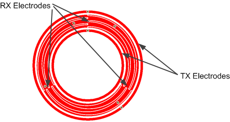
For reference, several self and mutual capacitive slider and wheel sensors examples are illustrated throughout this section and are the same sensors used on the CAPTIVATE-BSWP and CAPTIVATE-PHONE demo PCBs.
CapTIvate™ Technology's increased sensitivity combined with the CapTIvate™ Software Library provide exceptional linearity and accuracy for slider and wheel resolutions well beyond 10-bit of resolution. By following the design guidelines and examples that follow in this section, designing a slider or wheel with great performance is easy.
For sliders and wheels, the number of discrete positions = the resolution, but because 0 is included as a position, the reported range of positions covers from 0 to (resolution - 1). As an example, if a slider or wheel has a resolution of 1000, the sensor will report 1000 positions, from 0 to 999.
In general, self capacitive sensors are also easy to design and route on a PCB. Due to the nature of self-capacitance, self capacitive sliders and wheels have higher sensitivity compared to mutual capacitive sliders and wheels. For that reason they should be considered as a first choice when designing an application. However, self capacitive sensors require one CapTIvate™ I/O pin for each electrode.
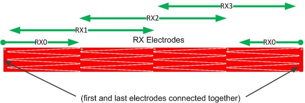
As mentioned above, a self capacitive slider with great performance can be designed with only three or four electrodes depending the size of the sensor. In fact, a 30cm slider using only four electrodes has been successfully demonstrated with superior linearity and resolution. A basic slider design below uses four RX electrodes. Each electrode is interdigitated and the two end electrodes are electrically connected.
A wheel is basically a slider design with both ends wrapped around and connected together. With CapTIvate™ Technology, a self capacitive wheel only needs three elements to provide execptional linearity and resolution. A basic wheel design below uses three RX channels. Each electrode is interdigitated.
Mutual capacitance has a unique feature that allows sensors to multiplexed. Mutual capacitive sliders and wheels can take advantage of this feature by sharing several RX channels with one or more sensors. Because of this, it is possible to have up to 64 electrodes using 16 CapTIvate™ I/O pins. As mentioned earlier, mutual capacitive sensor doesn't have the same sensitivity as a self capacitive slider or wheel. However, with CapTIvate™ Technology, mutual capacitive sliders and wheels will provide the same performance as self capacitive sensors.
The following diagram illustrates a four element slider. The outer TX electrode traces surround the interdigitaged RX electrodes and are connected together at both ends of the slider. This simple slider design uses four RX and one TX channels.
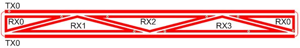
The diagram below illustrates a basic 3 element wheel design. The wheel has two TX circle electrodes surrounding the interdigitated RX electrodes. The wheel is basically a slider design with both ends wrapped around and connected together. This wheel design uses three RX and one TX channels.
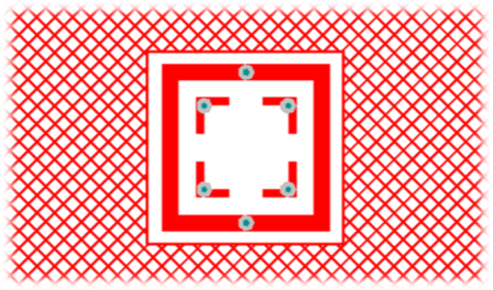
As a variation to the design above, the open portion of the wheel on the top PCB layer can be filled with either a solid or hatched ground to improve noise immunity. Providing a additional hatched ground on the bottom layer of the PCB will also help with noise. Using a solid ground on the bottom layer may present too much capacitive loading, so be careful.
A great feature to add is a separate "button" sensor inside the wheel sensor, if size permits. The design is the same as the basic wheel but a ground separation trace is added between the wheel electrodes and button electrodes. This helps prevent cross talk between the two sensors, should a finger wander slightly off the wheel sensor. This wheel design with center button uses three RX channels and one TX channel for the wheel, one RX and TX channel for the button.
Similar to the wheel design with a button in the center, it is simple to add a backlighted LED as illustrated in the next diagram. This wheel design with center LED uses three RX channels and one TX channel for the wheel. The LED is driven separately. For additional information about LEDs, refer to LEDs and Backlighting.
Proximity sensors are electrodes designed to detect a hand or other conductive object at some distance using greater sensitivity compared to buttons, sliders or wheels. For this reason, proximity sensors are self capacitive and can have one or more electrodes.
Proximity electrodes can be any shape and for most applications the electrode size is limited by the end product dimensions. As an example, the CAPTIVATE-BSWP Demo PCB with its proximity sensor highlighted in RED is shown below. As mentioned above, proximity sensors require a higher degree of sensitivity than buttons, and this higher sensitivity can be achieved by:
In a perfect design, without any parasitic capacitances, a proximity sensor's e-field can extend a great distance, providing incredible sensitivity. The field lines will flow from the electrode to any nearby ground potential and can include a nearby hand or earth ground.
Unfortunately, it is almost impossible to avoid having some ground potential on a PCB, so some charge is stolen away from the proximity sensor, reducing the sensor's sensitivity and detection distance.
One must be careful to avoid designs with excessive ground potentials. In some applications, where electrical noise is an issue, ground planes on top and bottom layers are in place to help shield circuits from potential noise sources. However, these very same ground planes that protect against noise now provide a very easy path to steal even more charge away from the proximity sensor, making proximity detection very difficult or even impossible.
One method to control the amount of parasitic capacitance to nearby ground is through the use of a driven shield. By replacing the dedicated ground plane with a plane driven by an additional CapTIvate™ I/O pin, the plane can be grounded through the I/O pin when the proximity sensor is not active. When driving the proximity sensor, the shield is also driven at the same potential. Any remaining parasitic capacitance to other ground potentials will steal charge from the shield and with minimal impact to proximity sensor's sensitivity. This minimizes the parasitic capacitance and restores the proximity sensor's sensitivity.
The MSP430 CapTIvate™ peripheral is capable of enabling user interface designs with extremely low power consumption. This is possible because the CapTIvate™ peripheral includes a processing state machine that is capable of performing the following functions from LPM3 without any CPU interaction whatsoever:
This capability combined with the MSP430 FRAM low power architecture enables designs with average current in the single digit microamps.
Designing for low power consumption involves optimizing the hardware and the tuning to achieve 5 basic things:
In short, achieving the lowest possible power consumption is all about optimizing the duty cycle of the application - minimizing the amount of time that the CPU and high performance analog are awake, and maximizing the amount of time spent in deep sleep.
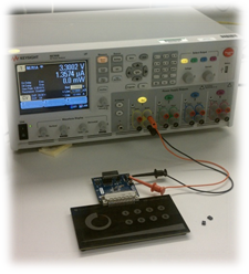
Below are several test cases that have been bench verified with the MSP430FR2633 on the CAPTIVATE-FR2633 processor module.
| Sensor Configuration | Mode | Method | Scan Rate | Base Scan Time | LF Clock | I-avg | I-avg / Electrode | Years on AAAs | Years on a CR2032 |
|---|---|---|---|---|---|---|---|---|---|
| 1 Proximity Sensor | Wake-on-Proximity | Self | 8 Hz | 420us | Crystal | 5uA | 5uA | 16 | 3.6 |
| 1 Proximity Sensor | Active (CPU) | Self | 8 Hz | 420us | Crystal | 7.3uA | 7.3uA | 10.9 | 2.5 |
| 1 Button | Wake-on-Proximity | Self | 8 Hz | 145us | Crystal | 3.4uA | 3.4uA | 23.5 | 5.3 |
| 1 Button | Active (CPU) | Self | 8 Hz | 145us | Crystal | 6.0uA | 6.0uA | 13.3 | 3.0 |
| 4 Buttons | Wake-on-Proximity | Self | 8 Hz | 120us | Crystal | 3.0uA | 750nA | 26 | 6.0 |
| 4 Buttons | Wake-on-Proximity | Self | 8 Hz | 145us | Crystal | 3.8uA | 0.9uA | 21 | 4.7 |
| 4 Buttons | Wake-on-Proximity | Self | 30 Hz | 145us | Crystal | 9.4uA | 2.4uA | 8.5 | 1.9 |
| 4 Buttons | Active (CPU) | Self | 8 Hz | 145us | Crystal | 8.7uA | 2.2uA | 9.2 | 2.1 |
| 8 Buttons | Active (CPU) | Self | 8 Hz | 145us | Crystal | 14.5uA | 1.8uA | 5.5 | 1.2 |
| 8 Buttons | Active (CPU) | Self | 15 Hz | 145us | Crystal | 25.9uA | 3.2uA | 3.0 | 0.7 |
| 8 Buttons | Active (CPU) | Self | 30 Hz | 145us | Crystal | 50.1uA | 6.3uA | 1.5 | 0.3 |
| 64 Buttons | Active (CPU) | Mutual | 8 Hz | 145us | Crystal | 109.2uA | 1.7uA | 0.7 | 0.2 |
| 64 Buttons | Active (CPU) | Mutual | 15 Hz | 145us | Crystal | 203.5uA | 3.0uA | 0.35 | 0.08 |
Note: These measurements were captured using a high resolution source-meter with UART/I2C communications disabled. Battery life was approximated assuming 1000mAh AAA's and 225mAh CR2032 cells with 70% effective usable life.
Note how the wake-on-proximity state machine is able to increase the battery life by over a year on a CR2032 coin cell for the proximity sensor, and over 2 years for a basic button.
The following sections discuss how to optimize the design to achieve the 5 goals introduced above.
The lowest power consumption achievable is limited by the deep sleep current consumption of the MCU. From there, power consumption will rise with the complexity of the panel and rate at which the panel is scanned. In deep sleep (low power mode 3), since it is not possible to achieve a lower average current than the LPM3 current, the low frequency clock that is selected for the application must be considered. Below are the available low frequency clock options for the MSP430FR2633 MCU.
| LF Clock Source | Typical LPM3 Base Current | Typical Frequency | Typical Relative Accuracy | Typical Relative Cost |
|---|---|---|---|---|
| Crystal | 1.2uA | 32768 Hz | Best | External Component (Highest) |
| REFO | 16uA | 32768 Hz | Good | Internal (Lowest) |
| VLO | 1uA | 10000 Hz | Poor | Internal (Lowest) |
The application scan period is the amount of time between each sampling of the user interface. For example, if the period is set to 100ms, then the user interface is sampled every 100ms, or at a rate of 10Hz. If the period is set to 10ms, then the user interface is sampled at a rate of 100Hz. The scan period has a direct effect on the power consumption, as it controls the duty cycle of the application. When a lower period (higher rate) is selected, the CapTIvate analog and possibly the CPU are waking up much more frequently- consuming more power. The design tradeoff here is response time versus power consumption. Scanning less often reduces the power consumption, but also increases the response time of the user interface. The CapTIvate™ starter project implements an active mode scan rate and a wake-on-proximity scan rate. This allows for a longer response time to be used when no one is touching the panel, and a shorter response time to be used when someone is touching the panel. The CAPTIVATE-BSWP demo panel runs at 10 Hz (100ms response time) when in wake-on-proximity mode, and at 30 Hz (33ms response time) when in active mode.
When a sensor has a low parasitic capacitance, it is more sensitive to touch (all else being equal). This means that the sensor may be scanned at a lower resolution to obtain the same resolution and SNR. A lower resolution conversion means a lower measurement time. Battery powered applications typically do not have the same noise immunity requirements as line powered applications, so solid ground fills that limit sensitivity are generally not required. In addition, when sensors have low parasitic capacitance the conversion frequency may be increased while still ensuring good charge transfer.
The measurement time for each sensor should be optimized to be as small as possible. When the CapTIvate™ analog IP is operational, it draws several 100uA of current. The goal should be to minimize the measurement time so that the analog is only enabled for a brief period of time.
In the CapTIvate™ Design Center, the measurement time is a function of the following factors:
The measurement time may be calculated manually per the following formula. It is also calculated automatically in the CapTIvate™ Design Center.
Constants
If the sensors have fairly low parasitic capacitance, a conversion frequency of 2MHz for self capacitance and 4MHz for mutual capacitance is a reasonable setting. With phase lengths of 1, this is achieved by setting the frequency divider to /4 and /2, respectively.
The conversion count controls the resolution of the measurement. Decreasing this value decreases the overall resolution of the measurement (in terms of counts per picofarad). To optimize the resolution, decrease this value until the minimum acceptable delta due to a touch is reached.
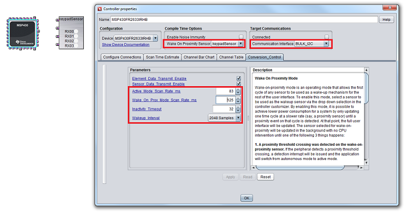
The wake-on-proximity state machine allows for CPU-less measurement and processing for 1 element per measurement block (4 elements total with the MSP430FR2633). Most sensing panels are actually touched <1% of the total time that they are running. 99% or more of the time, they are waiting for a user. The state machine provides a mechanism to handle the latter 99% without the need to involve the CPU, reducing the average current. A sensor may be selected as a wake-on-proximity sensor in the CapTIvate™ Design Center. When a sensor is selected, the starter project that is generated by the CapTIvate™ Design Center will transition into a wake-on-proximity mode whenever the inactivity timeout counter expires. In wake-on-proximity mode, the first cycle of the sensor that was selected for wake-on-proximity will be automatically measured by the state machine, and the CPU will not receive an interrupt until one of the following occurs:
The wake-on-proximity feature is best used with longer-range proximity sensors, such as the one on the CAPTIVATE-BSWP demo panel. However, if an MSP430FR2633 design has 4 buttons or less, it is possible to use the wake-on-proximity state machine functionality to wake up on any of the four buttons!
In this example, the CAPTIVATE-BSWP panel will be used as a piece of test hardware to look at how to optimize an imaginary application that has 4 buttons. From start to finish, going through this exercise will transform the average current of the solution from 100's of microamps to single digit microamps. To run the completed example, check out the UltraLowPower_4Button example project.
To start, a new CapTIvate™ Design Center project will be created that has a button group sensor with 4 buttons. The buttons will be on CAP0.0, CAP1.0, CAP2.0, and CAP3.0. This mapping allows for parallel scanning, which is important for power optimization. All of the default tuning parameters will be kept initially:
| Parameter | Value | Optimized? |
|---|---|---|
| COMM Peripheral | UART | No |
| Active Scan Rate | 33 | No |
| Wake-on-Proximity Scan Rate | N/A | No |
| Conversion Count | 500 | No |
| Frequency Divider | f/4 | Yes |
Out of all the default configuration values, only the frequency divider is optimized (f/4 with phase lengths of 1 for a conversion frequency of 2 MHz). This yields a starting, un-optimized current of approximately 310 uA-avg. We can do better than this! Note that LED1 and LED2 of the CAPTIVATE-FR2633 processor module must be disconnected, or the measured power will be higher.
UART requires that SMCLK be active for the baud rate generator to work. By switching to I2C for data transfer, we are able to go to LPM3 instead. This is possible because as a slave, the MSP does not need to provide a clock for I2C to operate.
| Parameter | Value | Optimized? |
|---|---|---|
| COMM Peripheral | Bulk-I2C (Slave) | Yes |
| Active Scan Rate | 33 | No |
| Wake-on-Proximity Scan Rate | N/A | No |
| Conversion Count | 500 | No |
| Frequency Divider | f/4 | Yes |
Making this change has lowered the current to 68 uA-avg. We can still do better! Note that the Design Center must be connected to see these power numbers, otherwise the I2C requests will time out, using more power.
The project came with a default conversion count of 500. This provides a delta due to touch of about 80 on the 4 buttons. This is more resolution than is needed. Lowering the conversion count to 200 and the conversion gain to 100 (to boost sensitivity) will cut the measurement time more than in half, and still provide a delta of about 30 counts. 30 counts is significantly less, but for button detection in a battery powered application, it is adequate. The default touch thresholds still work as well.
| Parameter | Value | Optimized? |
|---|---|---|
| COMM Peripheral | Bulk-I2C (Slave) | Yes |
| Active Scan Rate | 33 | No |
| Wake-on-Proximity Scan Rate | N/A | No |
| Conversion Count | 200 | Yes |
| Frequency Divider | f/4 | Yes |
These changes lower the current to 38 uA-avg. We are getting there.
The default scan period of 33ms provides good response time, but it uses power. Adjusting this down to 83ms (12 Hz) will reduce the power, but not so much that it compromises the ability to pick up a press.
| Parameter | Value | Optimized? |
|---|---|---|
| COMM Peripheral | Bulk-I2C (Slave) | Yes |
| Active Scan Rate | 83 | Yes |
| Wake-on-Proximity Scan Rate | N/A | No |
| Conversion Count | 200 | Yes |
| Frequency Divider | f/4 | Yes |
This change lowered the current to 26 uA-avg.
Now to add the final touches, let's enable the wake-on-proximity state machine functionality to manage states. We only have 4 buttons, with one from each measurement block, so we can measure all 4 buttons and test for proximity without any CPU involvement.
| Parameter | Value | Optimized? |
|---|---|---|
| COMM Peripheral | Bulk-I2C (Slave) | Yes |
| Active Scan Rate | 83 | Yes |
| Wake-on-Proximity Scan Rate | 125 | Yes |
| Conversion Count | 200 | Yes |
| Frequency Divider | f/4 | Yes |
The capture below shows the conversion control tab of the controller customizer, which contains most of the settings that we have been adjusting to optimize for low power.
This change lowered the current to 3 uA-avg, or about 750nA per button when no one is touching the panel. As soon as a user touches a button, the power consumption goes up to 23-26uA-avg with I2C reporting. Once the touch is removed, the UI goes back into wake-on-proximity mode after 32 samples and is back to the 3 uA-avg.
Mutual capacitance sensors have an extra tuning parameter: the bias current. During a mutual capacitance measurement, a sample-and-hold amplifier cancels out the effects of the parasitic / stray self capacitance on the receive electrode. This sample-and-hold amplifier has an adjustable bias current capability, which allows for the drive strength of the amplifier to be adjusted to suite the application.
For information on bias current settings how to adjust the bias current, see the bias current guide. Note that the bias current control is only available in advanced mode.
A larger bias current setting should be used when the parasitic capacitance to ground of the Rx electrode is large. The default value is the highest possible bias current, which works for the most applications but requires the highest power consumption. During low power optimization, it is desirable to lower the bias current if the layout allows for it. Most button designs with minimal parasitic capacitance work very well with the lowest bias current setting.
To optimize the bias current setting for a low power application, begin by setting the bias current to the lowest available setting. Test each electrode in the sensor for sensitivity to touch. One effect of setting the bias current too low is that a touch on a sensor will cause a decrease in counts rather than an increase, because the system cannot accurately compensate for the parasitic self capacitance of the receive (Rx) electrode. If this occurs, continue increasing the bias current until the behaviour goes away. Note that the bias current performance also varies with the conversion frequency. Higher conversion frequencies will require higher bias current settings for designs with more parasitic capacitance to ground.
This section discusses special considerations for designing products that will come into contact with moisture.
The performance of a capacitive touch panel can be effected by moisture spray and build-up, as well as liquid spills. In addition, self capacitance and mutual capacitance exhibit different phenomena depending on the nature of the moisture. For example, small water droplets on a self capacitance electrode may have little effect, but a water droplet on a mutual capacitance electrode may have the effect of improving the mutual coupling and creating a change in the measurement counts that goes the opposite direction of a touch. Interestingly still, a water droplet or spill on a self or a mutual capacitance electrode could cause a change in measurement counts in the direction of (rather than against) a touch, if the droplet or spill is also in contact with a nearby ground plane, power plane, or grounded electrode that is not being measured. This section will introduce the physics behind the effects of moisture, as well as some basic best practices to add a level of moisture resistance and detection to an application.
With careful attention to detail, it is possible to create designs that can reject small amounts of moisture. Through the use of guard channels, it is also possible to create designs that can detect spills and lock out the rest of the interface when a spill is detected.
Moisture build-ups and liquid spills that occur on panels in the real world affect capacitive sensing electrodes because the liquid on the panel exhibits electrical conductivity. Water is a polarized molecule, and in addition to its polarization, it is rarely pure and typically contains ions in solution. The amount of ions dissolved directly effects the conductivity of the moisture. Distilled water will appear to have much less of an effect than salt water or sweat, for example.
This conductive property means that moisture can appear to have a similar effect as placing a conductor (such as a piece of metal) on a panel. It's easy to understand how that will cause problems! Making things worse is the fact that moisture is unpredictable in multiple aspects:
At best, build-up of moisture occurs slowly over time and is tracked via environmental filtering. At worst, it happens unpredictably and quickly and triggers a false detection.
Because of the unpredictable nature of moisture, it is necessary to divide mitigation techniques into two types of applications: moisture tolerance and spill rejection.
| Application Type | Full Touch Detection | Spill Detection | Guard Channel Required | Typical Mechanical Mounting |
|---|---|---|---|---|
| Moisture Tolerance | Yes, typically | No | No | Vertical |
| Spill Detection | No, sensors are masked during a spill | Yes | Typically required | Horizontal |
Moisture tolerant applications include those which are able to operate with touch detection in the presence of steam, mist, and spray. Common applications include exterior/interior security panels, E-locks, thermostats, and car access keypads. Whether or not moisture tolerance is feasible for an application depends on the mechanical design and environment. Typically, the following must be true:
When designing a moisture tolerant application:
Spill rejection applications include those which are able to detect when a fluid spill has occurred on the sensing panel. Common applications are white goods such as a cooking surface control panel. The goal of spill rejection is not to enable full touch detection (which is extremely difficult when moisture or fluids cover multiple keys and/or ground), but simply to detect the presence of a spill and lock out the keypad until the spill is cleared by a user. This is most commonly achieved with the use of a guard channel, whose purpose is to detect large objects as well as spills.
When designing a spill detection application:
The CAPTIVATE-PHONE demonstration panel has a guard channel that is used for proximity sensing, palm rejection, and basic moisture rejection.
This section discusses how to design for electromagnetic compatibility.
Capacitive touch sensing involves the measurement of very small changes in capacitance of a sensing electrode. These changes are often on the order of a picofarad or less. Because the quantity being measured is so small, capacitive touch circuits that are going to be used in noisy environments must be designed with noise immunity in mind from the start. Often, potential noise sources may not even be known at the time of design. This chapter is dedicated to providing the necessary guidance to enable immunity to various types of noise. It introduces the most common noise threats to a capacitive touch system. For each threat, it discusses how to reduce the susceptibility of a capacitive touch circuit to that threat when using MSP CapTIvate™ MCUs.
If you are designing a system that will exist in a high noise environment, it is best to read and understand this guide before going through the process of schematic capture and layout design. It is strongly recommended that the Capacitive Sensing Basics chapter be read before reading this chapter.
The introduction section of the noise immunity guide establishes a knowledge base that will be used as a backdrop for the rest of the discussion. After the introduction, the following section will discuss several different noise problems (RF susceptibility, for example). Each problem will be introduced so that the phenomenon is understood. Finally, the last section will discuss the noise mitigation steps to apply to your design to provide robustness to all of the noise types discussed. The noise mitigation steps will be presented in the context of the Three Sided Approach. The noise mitigation steps section is the most important section, as it provides a check list of considerations to apply when designing for noise immunity. If you don't read the entire noise immunity guide, be sure to read the noise mitigation steps.
An aggressor-victim approach is taken to understand noise in a system. The diagram below illustrates this concept.
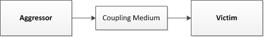
The aggressor is the noise source, which generates interference that affects the victim through the coupling medium. Generally speaking, for noise to couple from the aggressor to affect the victim, the following must be true:
Aggressor
The aggressor varies with every application. Common aggressors are poorly designed power supplies with high common-mode and differential-mode emissions, long cables and/or traces that act as antennas to radio frequency (RF) signals, and high-current switched inductive loads that share their power source with the victim at some level. In some cases, the viewpoint is such that the capacitive touch circuit is the aggressor.
Coupling Medium
The medium through which the noise travels from the aggressor to the victim is often misunderstood. Common mediums include the VCC rail, the VSS rail, the capacitive coupling between traces (in the case of crosstalk), and even users of the capacitive sensing interface themselves.
Victim
During most of the discussion in this chapter, the capacitive touch circuit is the victim. However, there are times where the capacitive touch circuit becomes the aggressor, at which time a neighboring subsystem may become the victim.
Based on this understanding, it becomes clear that to reduce the effects of the aggressor on the victim, it is necessary to fulfil one or more of the following objectives:
In some cases, it is possible to reduce the noise emitted by the aggressor (per the first bullet above). This is always the best course of action. Reducing the noise simplifies PCB layout and software considerations, and reduces the potential for other issues in the system. This is typically accomplished by designing robust power supplies and IO interfaces that do not generate their own noise nor pass on noise from the outside world. However, many times this is not possible because the aggressor may be outside the control of the system being designed. In that case, a solution must be obtained by reducing the coupling medium and reducing the victim's susceptibility.
Along these lines, to achieve a high level of noise immunity in a capacitive touch design it is necessary to apply the relevant CapTIvate™ peripheral features, hardware design principles, and signal processing tools. The basic tools available are listed below.
The general theme of this chapter is how these three main toolboxes (the CapTIvate™ peripheral, hardware design principles, and signal processing) may be applied together to solve several noise problems at the same time.
International standards exist to allow for consistent, repeatable electromagnetic compatibility testing to be applied to different products. The primary international standard concerning system level robustness in the area of EMC is the IEC 61000-4 family. The tests most relevant to capacitive touch circuits are introduced below, and will be addressed in detail later in this chapter.
The signal is the change in capacitance that results in a meaningful change in counts. Noise, on the other hand, is any disturbance that does not change the capacitance but does change the counts. Most often these disturbances are the result of power supply switching noise, electrostatic discharges (ESD), electrical fast transients (EFT), radiated RF noise, or some other type of electrical noise that couples into the system.
SNR is a system-level specification and needs to be tested at the system level. In achieving an acceptable level of SNR, the competing requirements for noise and signal must be addressed. The most common example of competing requirements is seen with ground shields. Ground shields help reduce susceptibility to radiated and conducted interference, and the closer these structures are to the circuit being protected, the more effective they are. However, moving these structures closer to the capacitive touch circuit has an unwanted effect of increasing the parasitic capacitance and consequently lowering the sensitivity.
In addition to managing the competing goals of sensitivity and noise immunity, these goals need to be managed within the overall requirements of the end product. This can mean trying to achieve a solution in a limited space, under a large aesthetic housing, or in the presence of other electrical activity (noise).
This section introduces the major types of noise that a capacitive sensing system may encounter. For each topic, the problem, MCU solution, and required design actions are discussed.
Differential-mode supply rail noise is any noise seen at the DVCC supply rail of the capacitive touch MCU with respect to the DVSS (circuit common) supply rail. Some touch solutions on the market require a dedicated LDO just for the capacitive touch circuit to reduce these issues.
Some of the problems associated with a direct reference to DVCC include:
To address these issues, the CapTIvate™ peripheral has low drop-out regulator that is dedicated to the capacitive sensing analog circuitry. This regulator provides decoupling from the supply rail (DVCC) as well as digital noise on-chip. Issue 1 above is resolved immediately, as the capacitive touch analog circuitry will always run at a constant, internally regulated voltage that does not drift with DVCC. The regulator is functional across the DVCC supply voltage range of the MCU (see the device datasheet for details). Issues 2 and 3 above are dramatically reduced as a result of the power supply rejection ratio of the dedicated regulator. While a dedicated regulator is not required, it does provide a compounded PSRR in very noisy systems and is still recommended.
In general, no specific action is required- the on-chip regulator provides the benefits described above.
Electrostatic discharge, if not properly managed, can disrupt a sample or even damage the MCU permanently. Fortunately, many tools exist to prevent this.
An electrostatic discharge involves a sudden flow of current between two charged objects. The flow of current may be caused by the breakdown of a dielectric material (such as plastic or even air), or direct contact. The voltage differential in a discharge may be on the order of several kilovolts (kV) or more. An electrostatic discharge applied to a device pin can permanently damage the device. Since capacitive touch panels by definition are interacted with by users or other objects that may be electrically charged, ESD deserves consideration during the design process.
The primary line of defense against ESD is always the touch panel overlay material. The overlay provides electrical isolation between the conductive electrode and any user or outside object that might interact with it. The ability of the overlay material to defend against ESD damage is dependent upon two main factors- the thickness of the material and its breakdown voltage, which is usually specified in terms of breakdown per unit of thickness. It is important to note that even if a discharge breaks down the dielectric material, the stress observed at the electrode (and possibly the device IO) will be less than the original stress on the overlay itself (since the breakdown accounts for some of the energy). Different materials will have different breakdown specifications. Generally speaking, plastics such as acrylic or polycarbonate have a higher breakdown voltage than materials such as glass. However, glass has a higher dielectric constant, which allows for better sensitivity through thicker overlays, allowing for both materials to be used easily.
Care should be taken to account for all places in a system that a discharge could slip through (say around the bezel of a product or through a ventilation gap). This is generally of more concern with products that have plastic enclosures than with those that have metallic enclosures that can be tied to an ESD ground or safety ground.
If it is not possible to obtain the needed protection mechanically, the next best alternative is to employ the use of series resistors on electrode pins, followed by low-capacitance TVS diode clamps if needed.
Electrical fast transients are common in industrial environments as well as within commercial products that contain switching inductive loads. These transients are similar in nature to ESD, but exhibit a lower magnitude and longer event length. When high-current inductive loads are switched on and off, high voltage transients may appear on power supply lines. Transients may also appear on signal lines if a system is connected to another system that is generating noise. The transients are a result of the inductance in the load that attempts to maintain the flow of current, and in so doing generates large voltages.
The IEC test simulates these threats by injecting bursts repetitively into the supply or signal lines of a system, in differential or common mode (though common mode is the most typical).
High voltage transients are one of the issues that must be considered ahead of time when designing the system. They can wreak havoc on simple analog circuits like the MCU reset circuit. However, with proper design techniques it is possible to realize designs with immunity to 4kV per the IEC 61000-4-4 test specification.
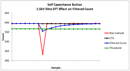
Fast transients can create effects similar to that of conducted noise, but generally only for brief periods of time as the duration of a transient is often quite short (on the order of 50 nanoseconds). This short burst time often means that not every capacitive touch sample will be affected by a burst. The figure below is data captured from a self capacitance button exposed to 1.5kV EFT bursts that were 50ns each. The 50ns transients were repeated at a 5kHz burst rate for 15ms. That pattern was then repeated every 300ms, per the IEC test specification. The different effects observed on the electrode can be attributed to the amount of time a sample may have overlapped with a 15ms burst window. There is about a 5% chance of a sample overlapping with a burst, due to the 300ms test period. It is important to note, however, that real world threats will likely not follow this pattern! The IEC test should be used as a tool to understand the implications of EFT on a system- but real world testing in-application is just as if not more valuable.
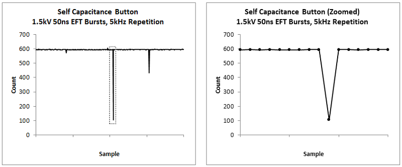
The primary line of defense against EFT must be hardware design. The best place to stop transients is at the power supply before they have a chance to effect different components of a product. Chances are good that the capacitive sensing MCU will not be the only component that is vulnerable to fast transients. Supplementing a good power supply, software should be EMC hardened. This includes de-bouncing the device reset pin, as well as implementing a watchdog timer. If EFT is a concern in a safety application, memory integrity self-tests should also be applied periodically for robustness. Heavy de-bounce of the capacitive touch sensor is also extremely valuable- almost more so than IIR filtering in an EFT environment. Take the figure below as an example. The EFT burst only affected a single sample- something a basic de-bounce can easily handle. However, the magnitude of the pulse was significant enough to pull down the IIR filter for more than one sample, overwhelming a de-bounce level of 1 and requiring a de-bounce level of 2+ or a weaker filter coefficient.
Capacitive touch circuits are inherently vulnerable to RF interference, since it can lead to injected noise currents into transmit (Tx) and receive (Rx) sensing IOs. By applying a combination of peripheral features, hardware techniques, and signal processing, it is possible to realize capacitive touch designs that are robust in the presence of RF interference.
RF interference will be broken down into two categories (conducted and radiated) based upon the frequency of the interference. The distinction between the two is important, as it defines the nature of the coupling medium between the aggressor and the victim. The breakdown is as follows:
In general, self capacitance sensors will allow for a higher level of noise immunity to be achieved than mutual capacitance sensors. This is a result of the fact that self-capacitance measurements are looking for larger changes (a few pF), whereas mutual capacitance measurements are looking for small changes (less than 1pF). In addition, to realize a mutual capacitance measurement the self-capacitance effect of the Rx must be eliminated from the measurement. This is achieved through the use of a sample-and-hold amplifier which compensates for the receiver (Rx) to ground capacitance to remove it from the measurement. If strong enough noise currents exist, this sample and hold amplifier can become overwhelmed to the point where it is not able to stabilize the Rx. When this happens, a self-capacitance effect (an overall decrease in counts) is observed. For this reason, self capacitance is the recommended method for high levels of immunity above 3Vrms. At or below 3 Vrms (the commercial product test level), mutual capacitance is a very viable sensing method with many advantages, such as higher key density.
The following table breaks down what kind of immunity can be expected when testing a system to the IEC 61000-4-6 specification.
Class A Immunity Table (Fully Functional in Presence of Noise)
| Sensing Method | Sensor Type | Achievable IEC 61000-4-6(Conducted) Level |
|---|---|---|
| Self | Buttons | Level 3 (10V RMS) |
| Self | Sliders/Wheels | Level 3 (10V RMS) |
| Self | Proximity | Level 1 (1V RMS) |
| Mutual | Buttons | Level 2 (3V RMS) |
| Mutual | Sliders/Wheels | Level 1 (1V RMS) |
| Mutual | Proximity | Not Recommended |
Conducted noise immunity is most reliably tested with the coupling/decoupling network method as specified in IEC 61000-4-6. A block diagram of the test configuration is shown below.
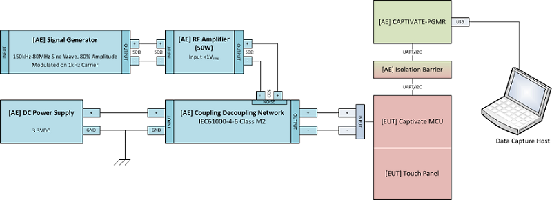
The frequency range tested is typically 150 kHz to 80 MHz, amplitude modulated at 80% depth on a 1 kHz carrier frequency to simulate real threats.
The problem with RF interference is that it leads to injected currents that can couple into receive (Rx) electrodes. Typically, the currents are common mode in nature with respect to some reference (usually earth ground). The adverse effects observed on capacitive touch circuits are different for self capacitance than for mutual capacitance, so the two will be treated separately in the following section.
Self capacitance sensors experience several different effects in the presence of noise depending upon the following factors:
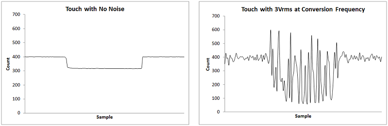
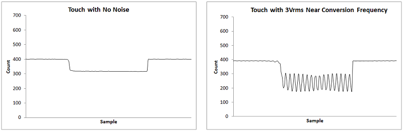
Mutual capacitance sensors exhibit corruption of data if noise is present at the conversion frequency or its lower harmonics. The susceptibility band is typically 100kHz around the conversion frequency. The effect can be seen in the diagram below.
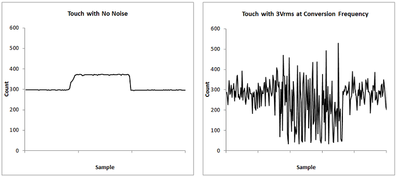
Notice how the data captured is completely unusable at this point. If the recommended layout practices are not followed, the result will be a widening of the susceptibility band in frequency beyond the typical value of ~100kHz. This will limit the performance of the frequency hopping solution described next.
Several methods are employed to improve immunity to conducted and radiated RF interference:
To achieve self-capacitance immunity, it is imperative that dense grounding structures be applied to limit fringing E-field lines. This has the effect of stabilizing the electrode. Then the use of frequency hopping and spread-spectrum clocking improves the data to a level where it may be processed by an algorithm, as shown below. In the plot below, noise is being injected at F3. Notice how F3 looks the same as the plot shown above in the problem section- it has positive and negative noise. However, F0-F2 are clean when no touch is present, and only exhibit the additional sensitivity in the negative direction when the button is touched. Applying spread-spectrum clock modulation reduces the effect of the noise at F3 to the point where it looks similar to F0-F2.
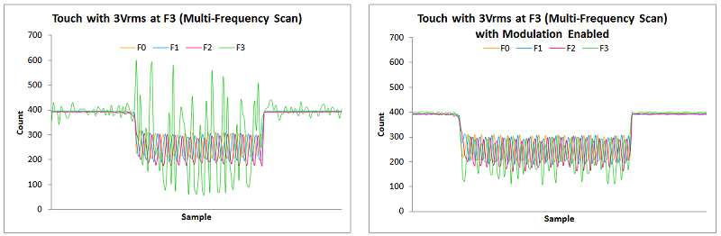
Taking that data set and applying the multi-frequency processing algorithm results in a fairly clean signal that may be filtered via the addition of the IIR count filter, as shown below. Notice that the signal still has an increased delta due to the injected noise current.
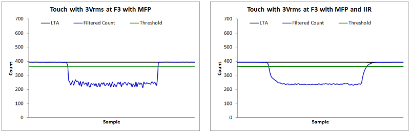
Now that a clean signal has been obtained, the noise level that was measured in the original raw data is used to compute a threshold adjustment factor via the dynamic threshold adjustment algorithm (DTA). This provides compensation for the slight gain in sensitivity due to noise in the system. The noise level is also reported, should it be of interest to the application. Below is a comparison of a no-noise touch and a touch in the presence of 3Vrms conducted noise at the base conversion frequency.
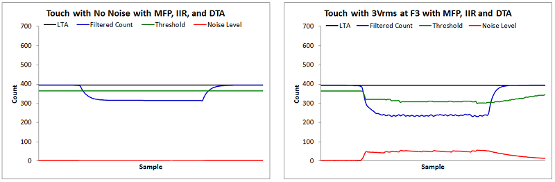
The application of all these design principles results in a button that dynamically responds to changes in the environment, compensating for noise. These techniques also work quite well on slider and wheel sensors.
As shown below, the application of frequency hopping and filter capacitors in mutual mode produces usable measurements at the auxiliary frequencies (left plot). The multi-frequency processing (MFP) algorithm may then resolve the data set into a usable count value that is fed into the standard element and sensor processing algorithms.
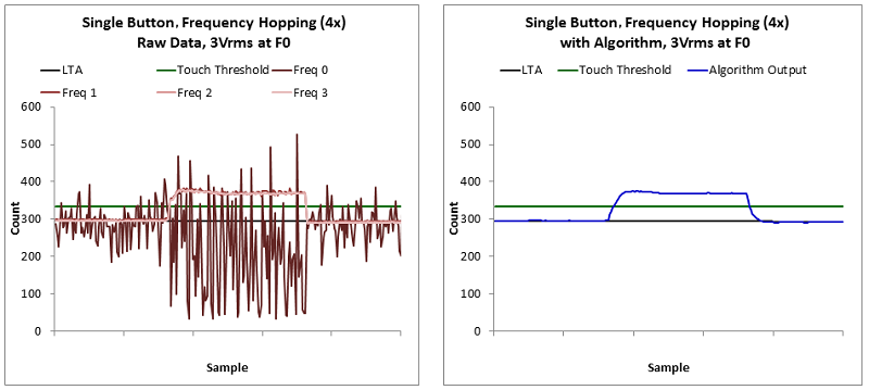
If the solution is looked at across a frequency sweep, the benefit of the frequency hopping approach becomes evident. This data set corresponds to a button that was not touched during the test.
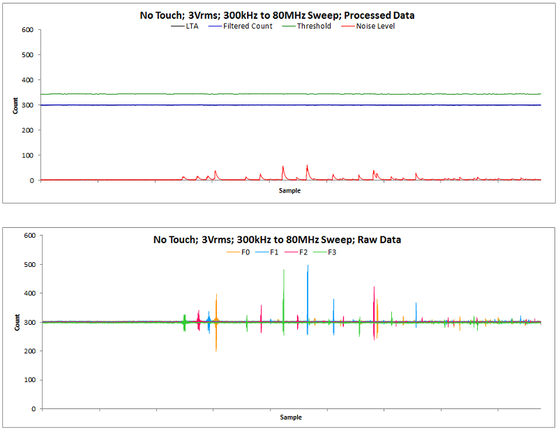
Note how the noise bands are very narrow, and are easily overcome by the frequency hopping algorithm. When touched, the susceptibility band increases and the amplitude of the noise increases. However, usable data is still obtained.
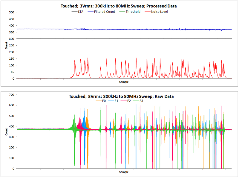
In both the untouched and touched diagrams, it is easy to pick out the fundamental frequencies at the left, and their corresponding harmonics. It may become obvious from reviewing the above diagrams that noise may affect more than one frequency at a time. In the event that this occurs, the frequency hopping approach is still able to handle most situations. The diagram below shows noise affecting two frequencies at the same time.
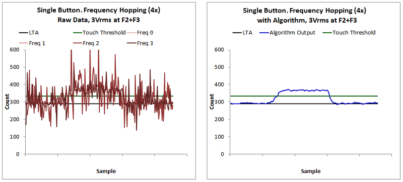
In the event that the noise become too great for the algorithm to determine what is happening, it is possible to use the noise threshold and noise status bits of the elements to alert the application and lock out a safety critical function.
Designing for immunity to RF interference does require hardware and software considerations. Be sure to review the final section of this guide, Noise Mitigation Steps, for implementation details.
One of the nice things about designing for EMC is that many of the techniques used to improve a design for one type of noise also tend to improve the design for other types of noise as well. This section steps through noise mitigation steps that should be applied to all designs that require noise immunity. It is best to think of this section as a design check list. All of the items discussed here should be applied when designing a product to have robust noise immunity.
Self capacitance is the recommended measurement method for designs that require sliders and wheels, as well as designs that need more than the commercial product level of 3Vrms conducted noise immunity. Mutual capacitance is recommended for designs that have higher key densities (16-32 buttons) and only require the commercial product immunity levels.
Review this check list before starting a PCB layout.
When designing for noise immunity, there are several best practices to apply to electrode geometry. Self capacitance and mutual capacitance will be discussed separately.
In the case of self capacitance, 3Vrms immunity is usually attainable without significant overhaul to the electrode design principles discussed in the button design section.
The following principles should be applied:
Below is a comparison of a standard button layout with the special button layout discussed in principle #5. The special button layout is really only suitable for designs with overlay stackups less than 3mm. Above 3mm, the sensitivity trade-off becomes too great.
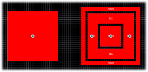
Mutual capacitance requires a specific geometry to achieve immunity. The layout below depicts the recommended geometry. The goals are as follows:
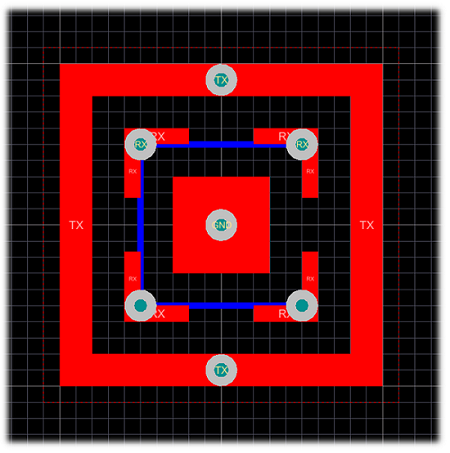
The geometry is as follows:
| Parameter | Value |
|---|---|
| Overall Geometry | 10mm x 10mm |
| Plane Keepout | 0.5mm from overall geometry on top layer, flooded on bottom layer |
| Tx Thickness | 1mm |
| Rx Thickness | 0.5mm |
| Inner Ground Fill | 3mm x 3mm |
| Tx to Rx Spacing | 1mm |
| Rx Wing Length | 2mm |
This electrode geometry has been proven with overlays between 1mm and 3mm of thickness.
Proper ground shielding of electrodes is required to achieve noise immunity. This applies to both self and mutual capacitance designs.
For self capacitance designs, utilize a solid ground or power plane on the top layer of the PCB, and a medium-density hatched power or ground plane on the bottom layer of the PCB. As an example, if the CAPTIVATE-BSWP panel (which was designed for low power battery operation) was modified to attain noise immunity, the following changes would be made:
Below are before and after images of the top and bottom layers, applying the principles described above:
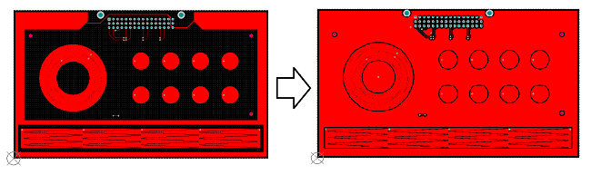
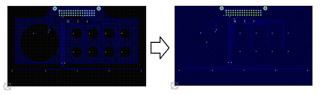
The addition of these dense ground structures serves to limit fringing E-field lines as much as possible, stabilizing the electrodes. Normally the addition of this much parasitic capacitance is considered bad practice, but in the case of noise immunity the trade-off is extremely beneficial. In addition, the gain and offset subtraction capability of the CapTIvate™ technology makes it possible to maintain decent sensitivity even with the ground shield structures.
For mutual capacitance designs, utilize solid ground or power planes on the top and bottom layer of the PCB. Mutual receive electrodes (Rx's) are extremely sensitive (on the order of <1mV). As a result, they are very vulnerable to noise currents. It is necessary to keep the Rx tracks as short as possible and as well-shielded as possible.
The design below illustrates these concepts for a 4x2 8-button mutual capacitance matrix:
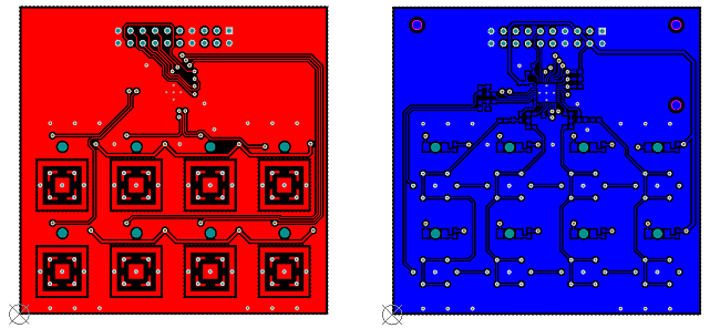
Review this check list when tuning a design that requires noise immunity.