
|
CapTIvate™ Technology Guide
v1.10.00.00
|
|
CapTIvate™ Technology Guide
v1.10.00.00
|
Capacitive touch evaluation and rapid prototyping has never been faster and easier. Using this modular kit with the CapTIvate™ Design Center, you can evaluate the performance of MSP430FR2633 MCU using the capacitive touch demo boards, or develop your own PCB and experience the power of the CapTIvate™ Design Center and the ease of real-time sensor tuning, all without writing a single line of code. Free software development tools are also available, including TI's Eclipse-based Code Composer Studio™ (CCS) and IAR Embedded Workbench® IAR-KICKSTART. Both of these integrated development environments (IDEs) support EnergyTrace™ technology when paired with the MSP430FR2633 MCU Development Kit.
Read through the overview section to become familiar with all of the hardware in the kit, or jump to the getting started section to begin evaluation.
The MSP-CAPT-FR2633 MCU Development Kit is an easy to use evaluation platform for the MSP430FR2633 microcontroller featuring CapTIvate™ Capacitive Touch Technology. It contains everything needed to start developing on the MSP430™ ultra-low-power (ULP) FRAM-based microcontroller (MCU) platform, including on-board emulation for programming, debugging and energy measurements. The MSP430FR2633 MCU features a new CapTIvate™ Capacitive Touch Technology, supporting self and mutual capacitive sensors, and embedded FRAM (ferroelectric random access memory). FRAM is a non-volatile memory known for its ultra-low power, high endurance, and high-speed write access.
The following PCBs are included in the kit:
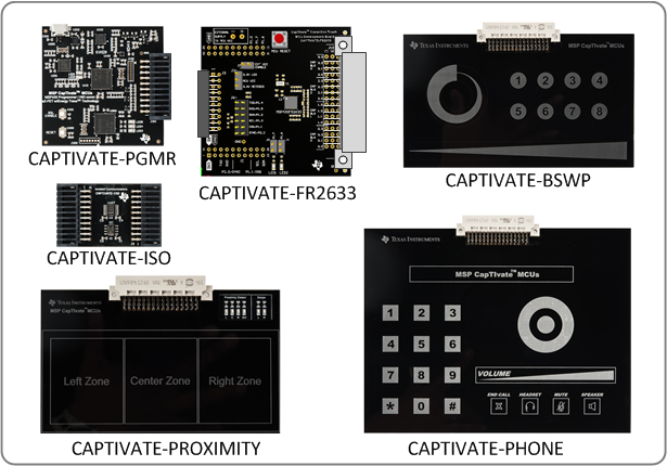
The follwing PCBs are available separately, but are compatible with this kit:
Complete CCS and IAR example projects for each demo panel are provided with the CapTIvate™ Design Center installation.
Schematic and layout design files for all of the PCBs in the kit are available from the MSP-CAPT-FR2633 product download page.
This section details how to get started with the development kit.
To get started with the kit, complete the following software and hardware steps:
Software Installation
Hardware Setup
Refer to the FAQ section for further troubleshooting tips.
Be sure that you have completed the pre work. The CAPTIVATE-FR2633 module ships pre-programmed with the demo software for the CAPTIVATE-BSWP panel. It is not necessary to program the target device to begin evaluating with that panel. Check out the workshop chapter for the out-of-box experience to begin working with the kit!
Be sure that you have completed the pre work. To run an example project, it is necessary to do the following:
This section describes each of the sensor panel demonstrations. For details on the hardware for each panel, visit the hardware section.
The CAPTIVATE-BSWP sensing panel demonstrates the low power and high sensitivity features of the CapTIvate™ technology. The wake-on-proximity state machine is utilized to measure the proximity sensor in LPM3 until a user is close to the panel. When a user is detected, all of the sensors begin scanning at a faster rate. Data is communicated to the CapTIvate™ Design Center via the bulk I2C interface.
This panel is configured with the following settings:
The typical memory requirements for this example when compiled using CCS are as follows:
| Memory Section | Requirement |
|---|---|
| FRAM | 6704B |
| RAM | 1641B |
This breaks down into the following major components:
| Memory Section | Object | Requirement |
|---|---|---|
| FRAM | main.c | 66B |
| FRAM | CAPT_App.c | 468B |
| FRAM | CAPT_BSP.c | 184B |
| FRAM | CapTIvate Software Library, MSP DriverLibrary, and MSP430 RTS Library | 5554B |
| FRAM | CINIT Table | 432B |
| RAM | Call Stack | 512B |
| RAM | CapTIvate Application Data | 1129B |
To begin working with this panel, go through the steps for running an example project and open the CAPTIVATE-BSWP project.
For an overview of the hardware design, visit the CAPTIVATE-BSWP hardware overview.
In addition to the out-of-box software project, the CAPTIVATE-BSWP panel is also used as the hardware platform for other examples that show off different features of the CapTIvate peripheral and MSP430FR2633 MCU.
This supplementary example project uses the first 4 buttons on the CAPTIVATE-BSWP panel only. It demonstrates how to achieve extremely low power consumption for a design that only contains 4 buttons.
This project is configured with the following settings:
The typical memory requirements for this example when compiled using CCS are as follows:
| Memory Section | Requirement |
|---|---|
| FRAM | 6376B |
| RAM | 1129B |
This breaks down into the following major components:
| Memory Section | Object | Requirement |
|---|---|---|
| FRAM | main.c | 34 |
| FRAM | CAPT_App.c | 468B |
| FRAM | CAPT_BSP.c | 184B |
| FRAM | CapTIvate Software Library, MSP DriverLibrary, and MSP430 RTS Library | 5554B |
| FRAM | CINIT Table | 136B |
| RAM | Call Stack | 512B |
| RAM | CapTIvate Application Data | 617B |
To begin working with this panel, go through the steps for running an example project and open the UltraLowPower_FourButtons project.
For a step-by-step workshop of how to reproduce this project from scratch, see the low power design example section of the design guide.
This supplementary example project uses the first button on the CAPTIVATE-BSWP panel only. It demonstrates a bare-bones touch application that just controls the state of the two LEDs on the MCU module. When the button is pressed, LED1 will illuminate and stay lit the entire time the button is pressed. At the beginning of each new press, LED2 will change its state.
This example serves as a reference for how to get down to a basic set of function calls. It achieves this by removing the CAPT_App layer that comes with the other example projects, and replacing it with register-level initialization of the MCU and top-level API calls directly into the CapTIvate library. This organization does not have support for the wake-on-proximity features, but it does have considerably reduced complexity as well as reduced memory requirements. This project easily fits into a small 8kB FRAM / 1kB RAM device variant.
Note: No communications module is included in the project build, so the only feedback will be visual via the LEDs!
The CapTIvate setup code is very basic, as shown below:
A simple background loop calls CAPT_updateUI directly and manages the use of the conversion timer interrupt flag variable.
A basic callback sets the LED states whenever the button is updated:
This project is configured with the following settings:
The typical memory requirements for this example when compiled using CCS are as follows:
| Memory Section | Requirement |
|---|---|
| FRAM | 3090B |
| RAM | 351B |
This breaks down into the following major components:
| Memory Section | Object | Requirement |
|---|---|---|
| FRAM | main.c | 240B |
| FRAM | CapTIvate Software Library and MSP430 RTS Library | 2760B |
| FRAM | CINIT Table | 90B |
| RAM | Call Stack | 256B |
| RAM | CapTIvate Application Data | 95B |
To begin working with this panel, go through the steps for running an example project and open the CodeSizeOptimized_OneButton project.
The CAPTIVATE-PHONE sensing panel demonstrates the use of mutual capacitance to realize a high-density panel with many different sensor types using just 12 of the 16 CapTIvate™ sensing pins. The panel is designed to mimic a typical office phone application that would have a 12-key numeric keypad, several mode buttons, and several selection sensors. The panel features haptic vibration feedback thanks to a TI DRV2605L haptic driver IC coupled with a Samsung linear resonant actuator (LRA). A guard channel technique is applied to reject palm/arm presses on buttons as well as minor liquid spills. Data is communicated back to the CapTIvate™ Design Center via a UART interface.
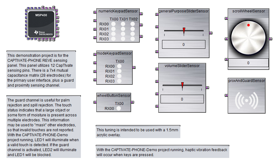
This panel is configured with the following settings:
This demonstration includes haptics to provide users with mechanical feedback that they did in fact touch a key. The most common and cost-effective actuators are the ERM (eccentric rotating mass) and LRA (linear resonant actuator). The LRA was chosen for this application because it provides a higher quality vibration feel than the ERM. For this reason, LRA's are more common with consumer products. However, there are some advantages to an ERM that are worth discussing here. LRAs have a limited lifetime of "clicks," and thus are not as suitable for long life cycle products as an ERM. Therefore, and ERM makes more sense than an LRA for long-life products such as industrial control panels.
With regard to the driver, The DRV2605L was selected as the driver IC for this demonstration for the following reasons:
The demonstration firmware includes an I2C master driver and a DRV26x driver for communicating with the DRV2605L. Setting up the DRV2605L with these modules is accomplished in the Demo_init() function as follows:
The callback capability of the CapTIvate™ Software Library is utilized to trigger playback of haptic events directly from the library. A sample callback function is shown below. Effects are fired on a "new" touch- if "touch" is true and "previous touch" is false. Note that the callback exits if the guard mask is active. This would be the case if the guard channel was in detect, and the touch on this sensor must be masked.
Below is a mapping of the various DRV2605L haptic effects that are mapped to the different sensors:
| Sensor | Element | Touchdown Effect | Continued Effect |
|---|---|---|---|
| numericKeypadSensor | All | Strong Click (100%) | None |
| modeKeypadSensor | Mute Button | Double Click (100%) | None |
| modeKeypadSensor | Speaker Button | Strong Click (100%) | None |
| modeKeypadSensor | Headset Button | Strong Click (100%) | None |
| modeKeypadSensor | End Call Button | Triple Click (100%) | None |
| wheelButtonSensor | Button | Pulsing Sharp 1 (100%) | None |
| scrollWheelSensor | Button | Buzz 1 (100%) | Soft Bump (100%) |
| generalPurposeSliderSensor | Button | Buzz 1 (100%) | Soft Bump (100%) |
| volumeSliderSensor | Button | Buzz 1 (100%) | Soft Bump (100%) |
| proxAndGuardSensor | Button | Smooth Hum 3 (30%) | None |
The guard channel is used as a detection mask for all other sensors in the system to provide a level of palm/arm rejection and spill rejection. The guard electrode wraps around the panel between all of the other sensors, and when it is not being measured, it serves as a grounded shield. The data from the guard channel is used to discern the case where a user accidentally puts their whole hand against the sensing panel. In that case, it would be very undesirable for all of the sensors to go into detect. It is also helpful in the event that the panel surface is being wiped down with a cloth or a liquid is spilled onto the panel.
Guard channel tuning requires the following considerations:
The two LEDs on the CAPTIVATE-FR2633 module indicate the status of the guard channel. When a valid touch is detected on an element, LED1 will illuminate. When the guard channel is active, LED2 will illuminate.
The example callback handler for the guard channel is shown below.
Note that the guard channel will not mask the reporting of touch and proximity events on other sensors to the CapTIvate™ Design Center. Rather, the mask is application-level and is used to control the haptic effect playback and LED illumination. The data flowing back to the design center provides the true state of each sensor at all times.
The typical memory requirements for this example when compiled using CCS are as follows:
| Memory Section | Requirement |
|---|---|
| FRAM | 7330B |
| RAM | 2150B |
This breaks down into the following major components:
| Memory Section | Object | Requirement |
|---|---|---|
| FRAM | main.c | 42 |
| FRAM | DRV26x driver, I2C Master driver, and application callbacks | 1126B |
| FRAM | CAPT_App.c | 204B |
| FRAM | CAPT_BSP.c | 184B |
| FRAM | CapTIvate Software Library, MSP DriverLibrary, and MSP430 RTS Library | 5014B |
| FRAM | CINIT Table | 760B |
| RAM | Call Stack | 512B |
| RAM | CapTIvate Application Data | 1638B |
To begin working with this panel, go through the steps for running an example project and open the CAPTIVATE-PHONE project.
For an overview of the hardware design, view the CAPTIVATE-PHONE hardware overview.
This example demonstrates standard distance-detection proximity as well as proximity gesturing. In addition, it demonstrates the use of a driven shield sensor to reduce the parasitic capacitance of large electrodes, improving their sensitivity. The module has 4 total electrodes- 3 on the top layer, and one large electrode around the 3 on the top layer and across the entire bottom layer. The large electrode acts as a shield for parasitic capacitance, while the 3 primary electrodes on the top layer perform the sensing. 6 LED indicators on the top of the module indicate the status of the panel.
This panel is configured with the following settings:
The 4 amber LEDs indicate prox detection on a given element (left, center, right, shield). Proximity is detected in the 5-10cm range, depending on the angle of approach.
The two green LEDs indicate whether or not a left or right swipe was detected above the panel. Waving your hand from left to right over the top of the panel triggers a right swipe, and waving from right to left triggers a left swipe. The LEDs are set after a valid swipe pattern is detected, and are cleared as soon as a new gesture is attempted by a new entry into the proximity field.
Gestures are detected through the use of a software state machine. All steps of the software state machine must be satisfied in order for a swipe to be detected.
| Step | Right Swipe Detection | Left Swipe Detection |
|---|---|---|
| 0 | No Detection | No Detection |
| 1 | Left | Right |
| 2 | Left Center | Right Center |
| 3 | Left Center Right | Right Center Left |
| 4 | Center Right | Center Left |
| 5 | Right | Left |
The typical memory requirements for this example when compiled using CCS are as follows:
| Memory Section | Requirement |
|---|---|
| FRAM | 6934B |
| RAM | 1133B |
This breaks down into the following major components:
| Memory Section | Object | Requirement |
|---|---|---|
| FRAM | main.c | 70 |
| FRAM | Swipe algorithm, callback function, LED control | 516B |
| FRAM | CAPT_App.c | 468B |
| FRAM | CAPT_BSP.c | 184B |
| FRAM | CapTIvate Software Library, MSP DriverLibrary, and MSP430 RTS Library | 5554B |
| FRAM | CINIT Table | 142B |
| RAM | Call Stack | 512B |
| RAM | CapTIvate Application Data | 621B |
To begin working with this panel, go through the steps for running an example project and open the CAPTIVATE-PROXIMITY project.
For an overview of the hardware design, view the CAPTIVATE-PROXIMITY hardware overview.
This example demonstrates the capacitive metal touch features of the CAPTIVATE-METAL PCB. For an overview of the hardware design, view the CAPTIVATE-METAL hardware overview.
This section provides detailed information about the hardware in the kit.
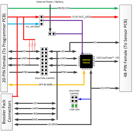
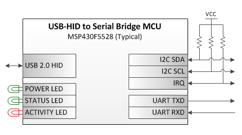
The CAPTIVATE-FR2633 PCB contains the MSP430FR2633 target microcontroller. Signals are brought in and out of the PCB in several different ways:
The connection routing is shown below:
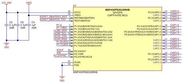
The MSP430FR2633 can operate from 1.8v to 3.6v, features up to 16-MHz system clock and 8-MHz FRAM access, 15.5KB of non-volatile FRAM and 4KB of data RAM. To help maximize the amount of FRAM code memory available to applications, the CapTIvate™ Software Touch Library, HID communications and MSP430-Driverlib I2C and UART drivers are provided in the 12KB of ROM and accessible through a simple API. Refer to the Software Library API for further details.
The CapTIvate™ capacitive touch technology supports self and mutual capacitive measurements on 16 I/O pins, with parallel scanning and up to 64 electrodes. This flexibility allows designers the freedom to mix self and mutual type buttons, sliders, wheels and proximity sensors into a single design.
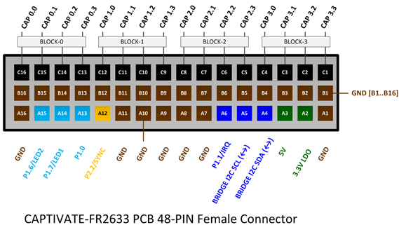
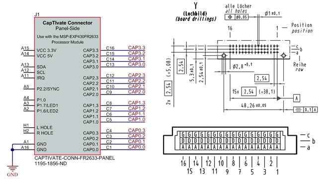
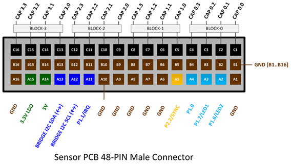
The female connector shown above makes available all of the MSP430FR2633 16 CapTIvate™ I/O channels, I2C, +3.3V, +5V and several general purpose I/O. The middle row of this connector is reserved for future devices that support up to 32 CapTIvate™ I/O channels. On this PCB, all of the pins on row-B are grounded.
For information on the 48-pin Male version of this connector, refer to the Sensor PCB Connector.
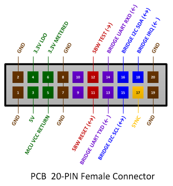
This female connector shown above is designed to connect with the CAPTIVATE-PGMR programmer PCB. This connector provides power, programming and communications between the two PCBs.
BoosterPack Connector Footprint
The CAPTIVATE-FR2633 provides a standard 40-pin BoosterPack connector footprint providing +3.3V, +5V, UART, I2C and 5 GPIO signals.
Suggested BoosterPack header/connector
Power
The CAPTIVATE-FR2633 PCB has two power sources available through the 20-pin connector J2 when attached to the CAPTIVATE-PGMR PCB. One source is a +3.3V (VCC_LDO) that provides power to the 48-pin connector J10 for devices such as LED drivers or Haptics drivers on a sensor PCB. The second source is the eZFET™ with EnergyTrace™ Technology DC/DC +3.3V output (VCC_METERED).
Target MCU power
Position the jumper J3 to pins(1-2) to select +3.3v LDO power source for the target MCU.
Measuring target MCU power
EnergyTrace™ Technology makes it possible to measure the power consumed by the target MCU when using CCS or IAR IDE. Position the jumper J3 to pins(2-3) to select +3.3v METERED power source for the target MCU.
Programming/Debug
The MSP430FR2633 MCU on this CAPTIVATE-FR2633 PCB is designed to be programmed and debugged through its Spy-Bi-Wire Interface. The full JTAG connection is not available on this PCB.
Note The eZFET™ back-channel UART feature is not supported on the CAPTIVATE-FR2633 PCB.
Communication
The MSP430FR2633 MCU communicates with a dedicated USB HID Bridge MCU located on the CAPTIVATE-PGMR PCB using UART or I2C communication to send sensor data and status to the CapTIvate Design Center as part of the sensor design and tuning process. A compact communications protocol is provided as part of the CapTIvate™ software library along with UART and I2C drivers. Both are located in the MSP430FR2633 ROM to minimize the impact on the FRAM memory footprint. The communications protocol is described in the HID Bridge Chapter.
When used with CapTIvate™ protocol, the UART operates in a full duplex mode using RX and TX pins, and the I2C operates as an I2C Slave using SDA and SCL pins with an additional pin P1.2/IRQ to generate interrupt requests.
Jumpers are provided to allow isolation between the MSP430FR2633 and the 20-pin Programming and Communications connector, if one or more of the I/O pins need to be re-purposed. Pull up resistors for I2C SDA, SCL and IRQ signals are provided on the "isolated" side of jumpers.
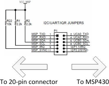
| Jumper | Description | Alternate Use |
|---|---|---|
| TXD | MSP430FR2633 UART data out | P1.4 |
| RXD | MSP430FR2633 UART data in | P1.5 |
| SDA | MSP430FR2633 I2C data in/out | P1.2 |
| SCL | MSP430FR2633 I2C clock input | P1.3 |
| IRQ | MSP430FR2633 I2C slave Interrupt out | P1.1 |
| SYNC | MSP430FR2633 CapTIvate™ Sync input | P2.2 |
Extended I2C Bus
The I2C signals are also present on the 48-pin sensor PCB connector. The I2C allows the MSP430FR2633 to control I2C slave devices, such as LED or Haptics drivers that might be installed on the sensor PCB.
Power Selection
Both VCC_LDO and VCC_METERED are routed to a selection jumper J3 which provides power to the MSP430FR2633 MCU. For most applications the VCC_LDO is recommended as it provides a very well regulated output. When the VCC_METERED output is selected, power consumed by the MCU can be measured using the EnergyTrace™ Feature in the CCS IDE.
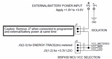
External / Battery Power
For battery powered applications, the MSP430FR2633 can be powered from an external 1.8V to 3.6V power source at the external power pads provided on the PCB. This allows the CAPTIVATE-FR2633 PCB and sensor PCB to be evaluated in an environment that is floating from any system or earth ground.
Caution When evaluating the MSP430FR2633 with an external power source, jumper J3 on the CAPTIVATE-FR2633 PCB should be completely removed. This prevents any conflicts between VCC_LDO or VCC_METERED from the CAPTIVATE-PGMR PCB and the external power source. However, as part of any normal development/debugging process the CAPTIVATE-PGMR and CAPTIVATE-FR2633 PCBs can be connected through the CAPTIVATE-ISO PCB. Using the CAPTIVATE-ISO PCB allows programming with debug as well as I2C and UART communications with the target MCU.
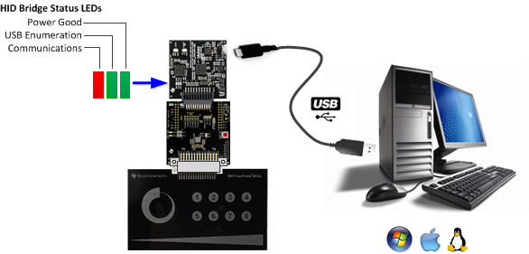
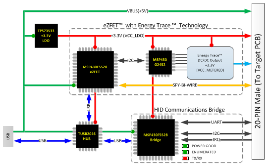
The CAPTIVATE-PGMR PCB provides debug services. It includes an eZ-FET with EnergyTrace and a HID Bridge for bringing UART and I2C into a host PC.
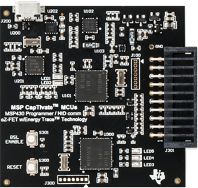
The male connector shown above is designed to connect with the CAPTIVATE-FR2633 MCU PCB. This connector provides power, programming and communications between the two PCBs.
Power
Power to the CAPTIVATE-PGMR PCB is provided through the USB connector at approximately 5VDC. A TI TPS73533 +3.3V, 500mA LDO provides power for all the devices on the CAPTIVATE-PGMR. This +3.3V output is referred to as VCC_LDO and is made available to the MSP430FR2633 target MCU on the CAPTIVATE-FR2633 PCB when attached. The eZFET™ with EnergyTrace™ Technology also provides a DC/DC +3.3V output. This output is referred to as VCC_METERED and is available only to the target MCU for energy measurements. A jumper on the CAPTIVATE-FR2633 PCB selects between the two sources for the MSP430FR2633.
Note: The CAPTIVATE-PGMR is considered a low-power USB device and therefore should draw at most 100mA. The CAPTIVATE-PGMR PCB draws a nominal 60mA. This allows any target to draw up to 40mA.
Programming/Debug
The eZFET™ provides programming and debugging through its Spy-Bi-Wire Interface.
The eZFET™ back-channel UART feature is available on this PCB, however, the CAPTIVATE-FR2633 does not support this feature.
Using Spy-Bi-Wire (SBW) programming with CAPTIVATE-ISO PCB Refer to JTAG and SBW Limitations
The CAPTIVATE-PGMR PCB features a HID-Bridge which enumerates as a USB HID device and does not require any drivers to be installed on the PC. It supports both I2C and UART interfaces and is factory programmed with a compact communications protocol for sending sensor data and status between the target MCU and the CapTIvate™; Design Center. For detailed information regarding the communications protocol, refer to HID Bridge Chapter.
Key features include:
The MSP430F5528 Bridge MCU supports firmware updates using USB BSL. To update the existing firmware or load a user-defined firmware image, use the "Python Firmware Upgrade" utility provided with MSP430ware. Depending on where MSP430ware has been installed on your computer, navigate to the "...\MSP430ware...\usblib430\Host_USB_Software\Python_Firmware_Upgrader" directory.
The CAPTIVATE-ISO PCB provides a way to maintain SBW, I2C, and UART communication when the CAPTIVATE-FR2633 target is powered from an external power source such as a battery or another system.
Important: To guarantee proper operation, power the "Target" side of the CAPTIVATE-ISO PCB with an external power source that meets the VCC minimum operating voltages shown in the table below. These values are provided for convenience only. Please consult the corresponding device's datasheet for more information.
| Isolator | Min Operating VCC |
|---|---|
| TI ISO1540 | 3.0 |
| TI ISO1541 | 3.0 |
| TI ISO7131 | 2.7 |
The maxium "Target" side voltage should not exceed the MSP430FR2633 VCC maximum operating voltage 3.6 VDC.
The CAPTIVATE-ISO PCB provides isolated Spy-Bi-Wire programming and debugging. Due to the added delays in the SBW timing, it is recommended to use the default medium JTAG/SBW speed or slower. JTAG/SBW speed = FAST is not supported at this time.
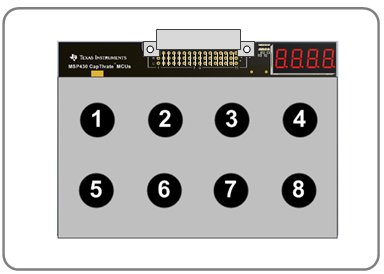
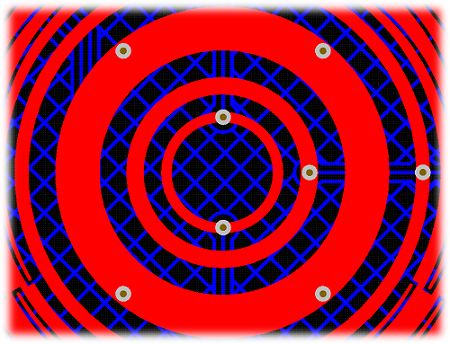
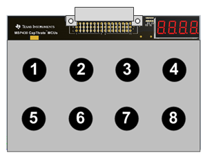
The CAPTIVATE-BSWP is a demonstration sensing panel with buttons, a slider, a wheel, and a proximity sensor. All of the sensors on this panel are self-capacitance sensors. The sensing panel serves the following purposes:
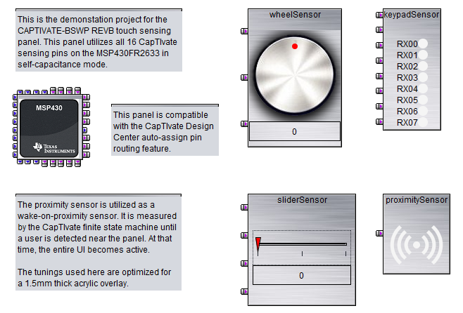
The 16 CapTIvate™ IOs are fully utilized by this panel. They are organized as shown in the diagram below.
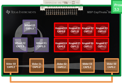
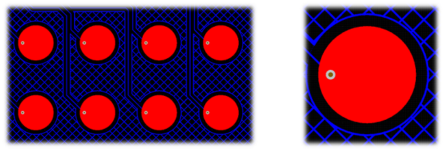
The button group sensor has 8 buttons, or "elements." They are connected to the following IO: CAP0.0, CAP1.0, CAP2.0, CAP3.0, CAP0.1, CAP1.1, CAP2.1, and CAP3.1. Note how the CapTIvate™ Design Center auto-assign feature selected two pins from each measurement block. This enables parallel scanning in 2 groups of 4 elements. Basic 10mm diameter circular electrodes were used for the buttons. A ground hatch was utilized underneath the electrodes, but was hollowed out underneath them to improve sensitivity and consequently power consumption, which was a design goal for this panel. For more information on button layouts, see the design guide.
The slider sensor has 4 elements. They are connected to the following IO: CAP0.2, CAP1.2, CAP2.2, and CAP3.2. Again, one pin was routed from each block to enable parallel scanning of the entire slider. This is very important for achieving the best possible linearity from a slider.
Linearity is define as the linear accuracy of the reported position of a slider or wheel sensor. It's a measure of how accurately the slider reports back position. For example, a touch in the center of a slider with 1000 points of resolution should return a value in the range of 490-510, not 400 or 600. Additionally, the slider should maintain that accuracy throughout the range of the slider. An example of poor slider performance would be what is called "stair stepping", where the position reported moves quickly, then slowly, then quickly again, all while a touch is moving at a constant rate.
By scanning all 4 slider elements in parallel, three performance improvements are attained. First, because each electrode is driven at the same voltage, there will minimal E-field between the electrodes. This reduces the parasitic capacitance of each electrode. If they had to be scanned sequentially, neighbouring electrodes would have to be grounded during a scan- meaning they look like a large parasitic capacitance. By scanning them in parallel, it is possible to tightly pack the electrodes together, optimizing surface area coverage and sensitivity. Second, there is no latency in the scan. With sequential scanning, by the time the 4th electrode is scanned the touch may be in a different location then when the first scan was performed- distorting the raw data that is fed to the position algorithm and reducing the accuracy of the slider to time changing touches. Third, the slider has common mode noise rejection because of the fact that all electrodes are scanned together. If noise effects one channel, it will affect all channels evenly. This has the overall effect of ensuring that a stable position is reported even in the presence of noise.
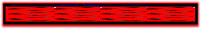
From a layout perspective, the inter-digitation of each element must be as linear as possible to enable linear position tracking. The performance of the slider is only as good as the layout. One feature of this slider is that the outer element is actually split into two pieces, one on each end, connected together to the same pin. The easiest way to think about this configuration is to think of it as a wheel that was "chopped" at the top, and unrolled to be flat. This provides the most linear performance, because the algorithm is going to resolve the slider back to a unit circle.
The proximity sensor that surrounds the slider is grounded during the scan of the slider. This serves to limit the interaction area to the slider, as fringing E-field lines from the edges of the sensor will be reduced because of the grounded sensor nearby.
The wheel has 3 elements. They are connected to the following IO: CAP0.3, CAP1.3, and CAP2.3. The design principles for the wheel are the same as for the slider.
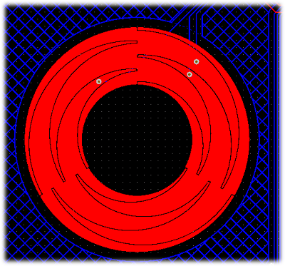
The proximity has 1 element connected to CAP3.3. The proximity sensor serves as a wake-up sensor for the rest of the panel. It was designed to wrap around the existing sensors already on the panel. By providing surface area around the existing sensors, it can detect when a user is close to any given sensor and use that information to wake the MCU from LPM3.
Note that there is no ground plane underneath of the proximity electrode. This was done intentionally to improve the sensitivity.
To explore the demonstration for this panel, check out the CAPTIVATE-BSWP demonstration section.
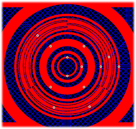
The CAPTIVATE-PHONE is a demonstration sensing panel with 17 buttons, 2 sliders, a wheel, and a proximity/guard sensor. There is also a DRV2605L haptic driver IC with a Samsung linear resonant actuator (LRA) for vibrational feedback. The sensing panel serves the following purposes:
Only 12 CapTIvate™ IOs are used for this demonstration, which has 29 elements! A mutual capacitance matrix made up of 4 Rx lines and 7 Tx lines (11 total pins) forms 28 elements. The 29th element is a self-capacitance guard channel and proximity combo sensor. The guard and proximity sensor is on CAP3.3. The 4 Rx lines are shared between all of the mutual capacitance sensors, and are connected to CAP0.0, CAP1.0, CAP2.0, and CAP3.0. Just like the CAPTIVATE-BSWP panel, selecting one receive line from each measurement block allows for efficient parallel scanning of 4 elements at a time.
The CAPTIVATE-PHONE demonstration utilizes the basic mutual capacitance button layout as shown in the design guide. This geometry is easy to lay out and provides more than adequate sensitivity for this application. Note that the guard channel is routed between the buttons. This will serve as a ground shield while the buttons are being measured.
The wheel selection button in the center of the wheel demonstrates how the geometry may also be radial with similar performance. Testing has revealed that E-field lines concentrate at the 90-degree corners of the square geometry, improving sensitivity. However, a radial geometry is still viable and is more applicable to the wheel button case because of the surrounding wheel sensor. Note that there is a ground fill between the wheel itself and the wheel button. This serves to provide shielding for the button, so that a touch on the edge of the wheel does not trigger the button.
The scroll wheel implementation on this PCB is effectively a condensed self-capacitance wheel for the Rx electrodes, with an inner and outer Tx ring forming the mutual coupling. This topology works quite well for creating a mutual capacitance wheel.
With slider and wheel design it is extremely important to match the parasitic capacitances as best as possible to ensure the best linearity. In the case of mutual capacitance, this means parasitic mutual capacitance. This type of parasitic shows up wherever Rx's and Tx's are brought close together. Usually it is straightforward to minimize trace parastics, but it can be difficult on larger PCBs such as this, or PCBs that have connectors. Drastic differences in parasitic capacitance lead to differences in sensitivity between electrodes in the slider or wheel, which will negatively impact the linearity. The CapTIvate™ technology calibration routine will reduce these effects to a certain extent, but it is always best to start with a good layout. Be aware of where your Rx's and Tx's come close together, and minimize these areas as much as possible by crossing them at 90-degree angles and placing ground between them if they run parallel to each other. This will serve to improve sensitivity as well as linearity.
The CAPTIVATE-PHONE sensing panel has two mutual capacitance sliders of different lengths. Both have 4 elements each based on the 4 shared Rx electrodes. The same layout technique is applied to both sliders, and it is quite easy to implement in most layout packages. Just like the scroll wheel, the Rx electrodes are encapsulated by two Tx tracks. Rather than the complex inter-digitation of the wheel layouts and the self-capacitance slider, a simple triangle design is implemented for this PCB.
Note that just like the self-capacitance slider on the CAPTIVATE-BSWP panel, the end elements are "half" elements, and they are connected together as if they were one full size element. This technique provides the pest performance from the position algorithm. If a smaller slider is desired, it is acceptable to drop an inner element at implement a 3-element slider using the same approach.
The proximity and guard sensor is simply a fill that flows in between all of the other sensor elements on the PCB. This is the only self-capacitance sensor on the panel.
From a proximity perspective, the electrode does not offer large sensing distances because it is directly above the ground hatch on the bottom layer. This creates a large parasitic capacitance on the order of 200pF, and it also reduces the E-field penetration into the area above the panel. A distance of a few centimetres is attainable- but not 5-10cm.
The guard channel functionality is essentially a re-purposing of the proximity sensor data. Because the proximity/guard electrode wraps around all of the sensors, it can be used as a detection mask for the other sensors. What this means is that when the guard channel reaches a certain level of interaction (the touch threshold), reporting of touches on other sensors is masked by the guard channel detection. This prevents other sensors from triggering if someone puts their whole palm down on the panel, or wants to wipe it down for cleaning purposes.
To explore the demonstration for this panel, check out the CAPTIVATE-PHONE demonstration section.
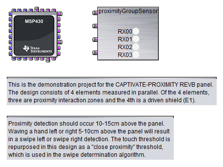
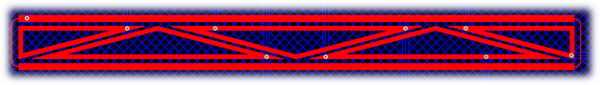
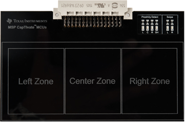
The CAPTIVATE-PROXIMITY is a demonstration proximity sensing panel with 4 electrodes. There are also 6 status LED indicators on the PCB: 4 for proximity detection, and 2 for gesture detection. The sensing panel serves the following purposes:
The module's 4 electrodes are connected to CAP0.3, CAP1.3, CAP2.3, and CAP3.3. CAP1.3 is used for the shield electrode, which is a solid plane across the bottom layer of the PCB and a ring around the 3 zones on the top layer of the PCB. CAP0.3, CAP2.3, and CAP3.3 are used to drive the left, center, and right zones, respectively. These three IO's are all dedicated capacitive sensing IO's- they are not muxed with GPIO functionality. As a result, they are not connected to the DVCC IO rail internally.While they have similar sensitivity when compared with muxed IO's, in theory they will be less effected by any switching noise that may be present on that rail due to a PWM, I2C, or other digital signal. All 4 electrodes are measured in parallel (one per sensing block).
Because all four electrodes are driven in parallel off of the same conversion clock, the potential difference between the various electrodes will be small. This means that the E-field between them (and thus, the result parasitic capacitance) will also appear quite small to the electrode. This parasitic reduction directly results in an improvement in overall sensitivity. It should be noted that the shield does not provide immunity to proximity interactions below the shield. If immunity to proximity on one side of an electrode is needed, a light (<20%) ground hatch is a better structure.
All demo sensor PCBs use the same 48 pin male connector that is commonly available from various manufacturers and suppliers. The following mechanical information will be useful if designing your own PCB to connect to the CAPT-FR2633 PCB. Below is a list of manufacturer part numbers:
| Manufacturer | Part No | Digikey No |
|---|---|---|
| FCI | 86093487313H55ELF | 609-4951-ND |
| Harting | 09 23 148 6921 | 1195-1856-ND |
| Harting | 09 23 148 2921 | 1195-1854-ND |
The HID Bridge is a multi-purpose development tool that provides a way to interface platform software (such as a PC GUI) with embedded systems containing basic serial interfaces (such as UART or I2C). The HID Bridge is a firmware product designed to run on an MSP430F5xx MCU with USB support. Typical implementations (such as the CAPTIVATE-PGMR) utilize an MSP430F5528 MCU.
The HID Bridge enables bidirectional transfer of data from a serial interface to a host platform via the USB HID device class. HID provides a unique advantage over other competing interfaces. Unlike USB CDC devices, no COM port identification is necessary on the host and no drivers are required on most modern operating systems. In addition, HID devices are much better suited to hot-swapping (disconnection and re-connection). During embedded system development it is very common to disconnect and re-connect development tools; using HID makes this process seamless.
The HID Bridge provides the following modes of operation:
The bridge enumerates on the USB host as a composite class human interface device (HID). Two HID devices enumerate:
The HID Bridge target UART interface is a bi-directional, full-duplex, two-wire UART interface that supports several common baud rates.
The baud rates supported are: 250kBaud, 115.2kBaud, 38.4kBaud, 19.2kBaud, and 9.6kBaud. The HID Bridge, when configured in UART mode, is constantly listing to the target UART port and may receive data at any time, even while it is transmitting data to the target. The UART baud rate is configurable via the HB command set.
The UART implementation also supports a "byte delay" feature for slow targets. This feature will insert a delay (in ms) between the start-of-transmission of each byte. This can allow a fast (250kBaud) rate to be used, but the bytes will be spaced out to allow the target to have time to service its UART interrupt service routine. When the target is sending data, it can still send at the full 250kBaud rate- but it doesn't have to respond do a datastream at that rate, because bytes will be spaced. The UART delay is configurable via the HB command set.
When configured in I2C mode, the HID Bridge acts as an I2C bus master that communicates with an I2C slave device.
The HID Bridge initiates writes to the target by initiating a start/write condition to the slave address that is selected, writing the data, and issuing an I2C stop condition.
The slave can request a read by pulling the I2C IRQ line low until the HID Bridge reads out the data from the target. Once the HID Bridge issues a start/read condition to the slave, the slave must release the IRQ line. The first byte read by the master is expected to be a length field that indicates to the HID Bridge how many further bytes it should read from the slave. The master will then continue the read, reading out that many bytes, then issuing a stop condition.
The HID Bridge is configured by the host platform through the sending and receiving of HID Bridge "HB" commands over the configuration console HID interface. The available configuration commands are described below.
| Command | Description | Arguments? | Valid Arguments (1) | ValidArguments (2) |
|---|---|---|---|---|
| HB VERSION | Get the version string. | None | - | - |
| HB PLATFORM | Get the platform string. | None | - | - |
| HB UPGRADE | Enter the USB bootloader. | None | - | - |
| HB REBOOT | Reboot the HID Bridge. | None | - | - |
| HB MODE | Get/set the operating mode. | Format, Interface | RAW, PACKET | UART, I2C |
| HB SAVECONFIG | Save the active or default configuration to boot memory. | Config to save | ACTIVE, DEFAULT | - |
| HB UARTBAUD | Get/set the UART baud rate. | New baud rate | 250000, 115200, 38400, 19200, 9600 | - |
| HB UARTDELAY | Get/set the UART byte delay period. | New delay period | 0 to 1000 | - |
| HB I2CADDRESS | Get/set the target I2C slave address. | New address | 0 to 127 | - |
| HB I2CCLOCK | Get/set the target I2C clock freq. | New frequency | 100000, 400000 | - |
For the commands that have no arguments, simply send "HB x" where x is the command. For commands with arguments, sending "HB x" where x is the command will echo back the current setting of that command, if supported. If valid parameters are passed (for example, "HB UARTBAUD 250000"), the parameter will be updated to the new value passed.
Note that the Captivate Design Center will automatically send configuration commands on this interface based on the current Design Center project that is open.
The HID bridge supports several different modes of operation as introduced above. The details behind how each mode behaves are described in this section. The operating mode may be set via the HID Bridge command set.
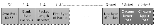
Packet mode requires that data sent over the target interface be formatted in packets according to the following set of transmission rules. The HID Bridge will buffer all data received from the target. It will then identify and frame packets to be sent to the host. When sending packets to the host, each packet will be transmitted in its own HID report. The HID Bridge buffers all packets coming from the host, and applies the relevant transmission rules before sending the packet on to the target.
If any transactions are of the following type, they are subject to the transmission rules:
The transmission rules for the serial interface in packet mode are as follows:
Per these rules, a packet would have the following format:
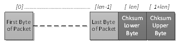
All other packet types (the remaining types are listed below), only require that a checksum be appended to the payload.
Note that the HID Bridge strips out the transmission rule overhead (if applied) when sending the payload and checksum on to the host. The SYNC, BLANK, and LENGTH bytes are removed, and any stuffed bytes in the payload section are removed. The checksum is preserved and is sent on.
In all cases, when the HID Bridge is in PACKET mode, the checksum field must be valid or data will not be sent on. For example, if a packet is sent from a target to the HID Bridge, and the checksum is invalid, that packet will not be sent on to the host. Likewise, if the host sends a packet to the HID Bridge, and the checksum is invalid, that packet will not be sent on to the target.
When operating in RAW mode, the HID Bridge basically acts as a communication buffer. No formatting is required. Any data received from the target is sent on to the host, and any data received from the host is sent on to the target. There is no HID frame alignment on the host side.