Communication Protocol Spec
Abstract
The Energy Measurement Design Center (EMDC) communication protocol is similar to the CapTIvate protocol but instead transmits configuration data, calibration data and energy measurement data. The EMDC GUI uses this protocol to communicate with a supported MSP430 MCU through a USB HID Bridge. This HID Bridge converts USB packets on the host (PC) side to/from UART packets on the target (MSP430) side. The default UART baud rate settings are provided in the next section. In designs where the host is an embedded processor or another MCU, the EMDC protocol can be implemented on the host to communicate with a MSP430 MCU running the Energy Measurement software library. A USB HID Bridge would not be required in that case. This document discusses the details of the protocol: packet types, packet structure, and transmission.
Default UART Settings
This section describes the default UART settings for the EMDC communication protocol. Please note that the EMDC GUI adds a 1 ms delay between sent packets to allow enough time for the target MSP430 MCU to receive and process them.
Baud rate: 250k baud
Data bits: 8
Parity bit: None
Stop bits: 1
Commands Overview
This section describes the commands exchanged between EMDC and the target MCU.
Commands from EMDC to Target
The following commands have API handlers on the target side:
Configure Mode (0x01) - EMDC configures the application mode (IDLE, ACTIVE, CALIBRATION).
Application Version (0x02) - EMDC reads device and firmware ID.
Request Calibration Values (0x03) - EMDC requests the target to send all the calibration values. When the target is done it will send this command with the calibration request flag set to done.
ADC Buffer Size (0x04) - EMDC reads the current and voltage buffer sizes to calculate the maximum and minimum preload allowed during calibration.
Calibration Values (0xB0) - EMDC writes the calibration values to the working (RAM) calibration structure for Phase ID.
Calibration Phase Configuration (0xB1) - EMDC configures the Phase ID being calibrated. After this command is received the target will send phase results. In CALIBRATION mode results will not be sent to the EMDC until this command is received. The Phase ID is cleared in the target when the application switches back to ACTIVE mode.
Calibration Values Save (0xB2) - EMDC requests target to store calibration values for Phase ID in Flash. When the target is finished writing to Flash it will send this command with the Flash Write Flag set to true.
Note The results commands do not have an API handler on the target. After EMDC configures the application mode to ACTIVE, then the target will send all the results for each phase to EMDC.
Commands from Target to EMDC
The following commands are handled by the EMDC HID interface:
Application Version (0x02) - The target sends device and firmware ID after EMDC has sent this command in READ mode.
Request Calibration Values (0x03) - The target sends calibration request flag after it finishes sending all the calibration values to EMDC. This allows the application to know when all the calibration values have been sent by the target.
ADC Buffer Size (0x04) - The target sends the current and voltage buffer sizes.
VRMS Result (0x80) - The target sends the VRMS result (mV).
IRMS Result (0x81) - The target sends the IRMS result (uA).
V Peak Result (0x82) - The target sends the Voltage Peak result (mV).
I Peak Result (0x83) - The target sends the Current Peak result (uA).
Power Factor Result (0x84) - The target sends the Power Factor result.
Frequency Result (0x85) - The target sends the Frequency result (1x10⁻² Hz).
Active Power Result (0x86) - The target sends the Active Power result (uW).
Reactive Power Result (0x87) - The target sends the Reactive Power result (uVAr).
Apparent Power Result (0x88) - The target sends the Apparent Power result (uVA).
Active Energy Result (0x89) - The target sends the Active Energy result (uWh).
Reactive Energy Result (0x8A) - The target sends the Reactive Energy result (uVArh).
Apparent Energy Result (0x8B) - The target sends the Apparent Energy result (uVAh).
Calibration Values (0xB0) - The target sends the calibration values stored in working (RAM) memory for Phase ID to EMDC.
Calibration Values Save (0xB2) - The target sends the Flash Write Flag set to true after it finishes writing calibration values.
Protocol Overview
This section will explain how the protocol used between the EMDC and target using the commands previously explained using sequence diagrams.
The “Initial Commands Exchanged” figure shows the commands exchanged between EMDC and the target after the HID communication is established between EMDC and the hid bridge board. After these commands are sent the target will continue sending results for all the phases supported.
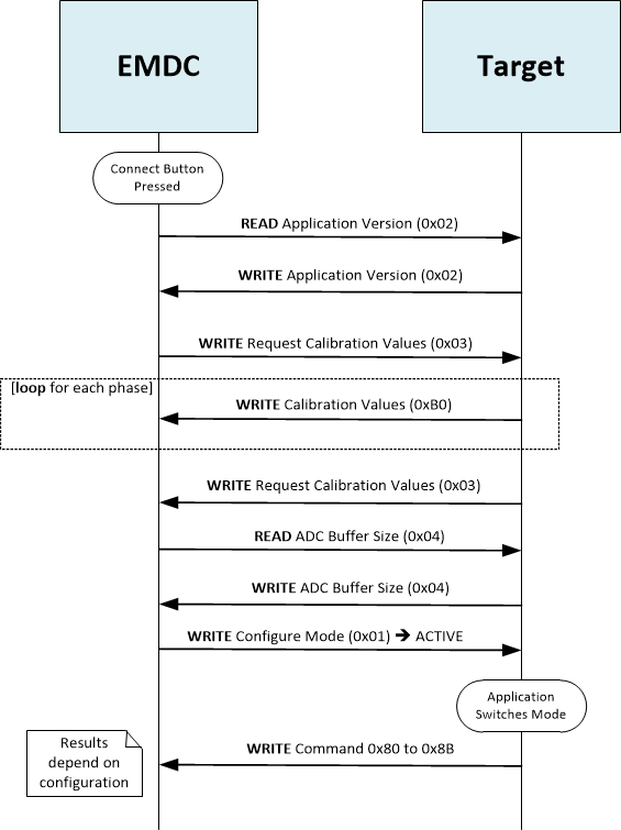
Fig. 129 Initial Commands Exchanged
The “Disconnect Commands Exchanged” figure shows the command sent from EMDC to the target at any time the Disconnect button is pressed on the GUI.
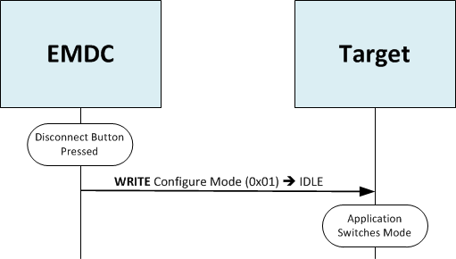
Fig. 130 Disconnect Commands Exchanged
The “Calibration Commands Exchanged” figure shows the commands exchanged between EMDC and the target when the user is initializing phase calibration mode on the GUI. Once the Calibration Phase Command is sent to the target, the target will continue sending results for the phase being calibrated. When the Apply Button is pressed the GUI will write the values to RAM and re-configure the SD24 (for phase calibration). The next set of results sent to EMDC will take into account the new calibration values. Once the phase has been calibrated and the user clicks the stop button, there will be an option to save the calibration results in Flash. If the user selects Yes, then the calibration values will be stored in Flash while all the global interrupts are disabled. Otherwise, the EMDC will configure the target in ACTIVE mode.
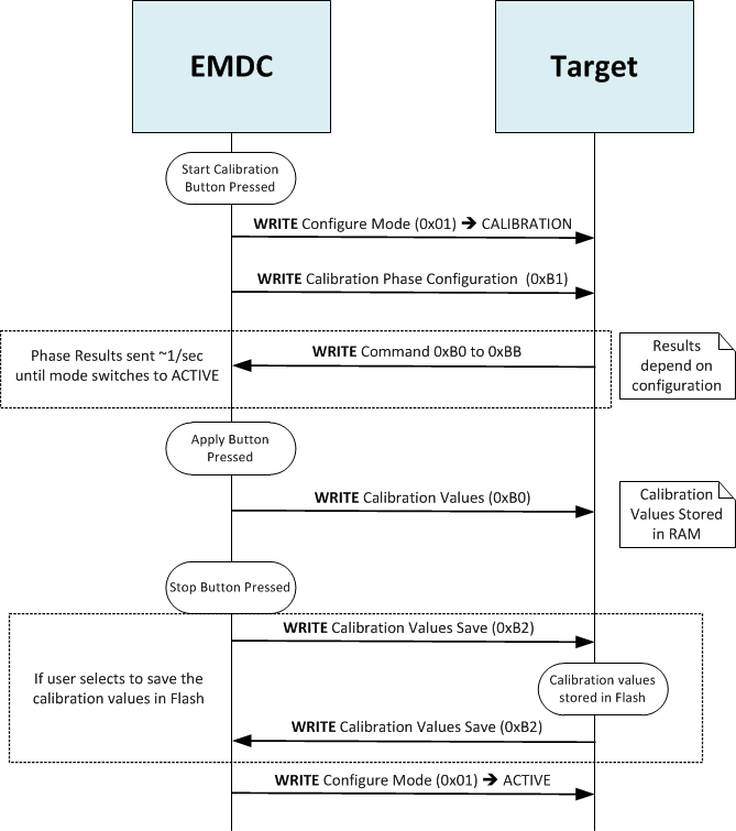
Fig. 131 Calibration Commands Exchanged
EMDC Packet Overview
Generic Packet Structure
Header | Control | Data | Checksum | |||||||
|---|---|---|---|---|---|---|---|---|---|---|
[0] | [1] | [2] | [3] | [4] | [5] | [6] | … | [N] | [N+1] | [N+2] |
SYNC | BLANK | LENGTH | DESIGN CENTER ID | COMMAND ID | READ/ WRITE | PAYLOAD LSB | … | PAYLOAD MSB | CHECKSUM LSB | CHECKSUM MSB |
Generic Packet Description
Byte # | Name | Description |
|---|---|---|
[0] | SYNC | Indicates the start of a new packet, always 0x55. |
[1] | BLANK | Not equal to 0x55, typically 0xAA. |
[2] | LENGTH | Equal to total size (in bytes) of the Control, Data and Checksum packet sections. |
[3] | DESIGN CENTER ID | Identifies packet as a command for a specific Design Center GUI. For EMDC, this byte is always 0x04. |
[4] | COMMAND ID | Specifies command type. Each command has a fixed length. See section below for command descriptions. |
[5] | READ/WRITE | Specifies if a command should be performed as a read or write operation: 0x00 for read, 0x01 for write. |
[6] to [N] | PAYLOAD | Contains binary data. The Control and Data packet sections may contain up to 60 bytes. If the SYNC byte (0x55) occurs in these sections, it must be sent again to distinguish it from a true SYNC byte. This repeated byte does not count towards the maximum size of 60 bytes. |
[N+1] to [N+2] | CHECKSUM | Contains lower unsigned 16 bits of the sum of the bytes in the Control and Data packet sections, excluding any repeated SYNC (0x55) bytes. |
Configuration Parameters Description
All Result Parameter (Commands 0x01 to 0x04) contains 1 to 2 payload bytes. This section will describe the packet structure for each Configuration Parameter command.
Command 0x01 (Configure Mode)
Byte # | Description | Data Type | Valid Value/Range | Notes |
|---|---|---|---|---|
[3] | Design Center ID | uint8_t | 0x04 | |
[4] | Command | uint8_t | 0x01 | |
[5] | Read/Write Command | uint8_t | 0x00 == Read, 0x01 == Write | |
[6] | Application Mode | uint8_t | 0x00 == IDLE, 0x01 == ACTIVE, 0x02 == CALIBRATION, 0x03 to 0xFF (Reserved) | IDLE = No results sent to EMDC, ACTIVE = Results for all phases transmitted to EMDC, CALIBRATION = Results from the phase being calibrated transmitted to EMDC |
[7] to [8] | Don’t care | N/A | N/A |
Command 0x02 (Application Version)
Byte # | Description | Data Type | Valid Value/Range | Notes |
|---|---|---|---|---|
[3] | Design Center ID | uint8_t | 0x04 | |
[4] | Command | uint8_t | 0x02 | |
[5] | Read/Write Command | uint8_t | 0x00 == Read, 0x01 == Write | |
[6] | Device ID | uint8_t | 0x01 == MSP430i2021, 0x03 == MSP430i2031, 0x05 == MSP430i2041, 0x25 == MSP430F6736, 0x2B == MSP430F6736A, 0x74 == MSP430F6779, 0x79 == MSP430F6779A, 0x84 == MSP430F67791, 0x89 == MSP430F67791A | |
[7] | Firmware ID | uint8_t | Firmware version | |
[8] to [9] | Don’t care | N/A | N/A |
Command 0x03 (Request Calibration Values)
Byte # | Description | Data Type | Valid Value/Range | Notes |
|---|---|---|---|---|
[3] | Design Center ID | uint8_t | 0x04 | |
[4] | Command | uint8_t | 0x03 | |
[5] | Read/Write Command | uint8_t | 0x00 == Read, 0x01 == Write | |
[6] | Calibration Request Flag | uint8_t | 0x00 == Target has NOT received a request to send calibration values, 0x01 == Target has received a request to send calibration values, 0x02 == Target has transmitted all the phase calibration values to EMDC | |
[7] to [8] | Don’t care | N/A | N/A |
Command 0x04 (ADC Buffer Size)
Byte # | Description | Data Type | Valid Value/Range | Notes |
|---|---|---|---|---|
[3] | Design Center ID | uint8_t | 0x04 | |
[4] | Command | uint8_t | 0x04 | |
[5] | Read/Write Command | uint8_t | 0x00 == Read, 0x01 == Write | |
[6] | Phase Voltage Array Size | uint8_t | Multiple of 2 | -1 x Size x OSR = minimum total preload used in calibration |
[7] | Phase Current Array Size | uint8_t | Multiple of 2 | Size x OSR = maximum total preload used in calibration |
[8] to [9] | Don’t care | N/A | N/A |
Result Parameters Description
All Result Parameters (Commands 0x80 to 0xAF) contains 5 to 9 payload bytes. This section will describe the packet structure for each Result Parameter command.
Command 0x80 (VRMS Result)
Byte # | Description | Data Type | Valid Value/Range | Notes |
|---|---|---|---|---|
[3] | Design Center ID | uint8_t | 0x04 | |
[4] | Command | uint8_t | 0x80 | |
[5] | Read/Write Command | uint8_t | 0x00 == Read,> 0x01 == Write | |
[6] | Phase ID | uint8_t | 0x01 == Phase A, 0x02 == Phase B, 0x04 == Phase C, 0x08 == Phase D, 0x10 == Phase E, 0x20 == Phase F, 0x40 == Neutral, 0x80 == Total | |
[7] to [10] | RMS Voltage (mV) | uint32_t | 0x0000 to 0xFFFF FFFF | Byte [7] is LSB, Byte [10] is MSB |
[11] to [12] | Don’t care | N/A | N/A |
Command 0x81 (IRMS Result)
Byte # | Description | Data Type | Valid Value/Range | Notes |
|---|---|---|---|---|
[3] | Design Center ID | uint8_t | 0x04 | |
[4] | Command | uint8_t | 0x81 | |
[5] | Read/Write Command | uint8_t | 0x00 == Read, 0x01 == Write | |
[6] | Phase ID | uint8_t | 0x01 == Phase A, 0x02 == Phase B, 0x04 == Phase C, 0x08 == Phase D, 0x10 == Phase E, 0x20 == Phase F, 0x40 == Neutral, 0x80 == Total | |
[7] to [10] | RMS Current (uA) | uint32_t | 0x0000 to 0xFFFF FFFF | Byte [7] is LSB, Byte [10] is MSB |
[11] to [12] | Don’t care | N/A | N/A |
Command 0x82 (V Peak Result)
Byte # | Description | Data Type | Valid Value/Range | Notes |
|---|---|---|---|---|
[3] | Design Center ID | uint8_t | 0x04 | |
[4] | Command | uint8_t | 0x82 | |
[5] | Read/Write Command | uint8_t | 0x00 == Read, 0x01 == Write | |
[6] | Phase ID | uint8_t | 0x01 == Phase A, 0x02 == Phase B, 0x04 == Phase C, 0x08 == Phase D, 0x10 == Phase E, 0x20 == Phase F, 0x40 == Neutral,> 0x80 == Total | |
[7] to [10] | Voltage Peak (mV) | uint32_t | 0x0000 to 0xFFFF FFFF | Byte [7] is LSB, Byte [10] is MSB |
[11] to [12] | Don’t care | N/A | N/A |
Command 0x83 (I Peak Result)
Byte # | Description | Data Type | Valid Value/Range | Notes |
|---|---|---|---|---|
[3] | Design Center ID | uint8_t | 0x04 | |
[4] | Command | uint8_t | 0x83 | |
[5] | Read/Write Command | uint8_t | 0x00 == Read, 0x01 == Write | |
[6] | Phase ID | uint8_t | 0x01 == Phase A, 0x02 == Phase B, 0x04 == Phase C, 0x08 == Phase D, 0x10 == Phase E, 0x20 == Phase F, 0x40 == Neutral, 0x80 == Total | |
[7] to [10] | Peak Current (uA) | uint32_t | 0x0000 to 0xFFFF FFFF | Byte [7] is LSB, Byte [10] is MSB |
[11] to [12] | Don’t care | N/A | N/A |
Command 0x84 (Power Factor)
Byte # | Description | Data Type | Valid Value/Range | Notes |
|---|---|---|---|---|
[3] | Design Center ID | uint8_t | 0x04 | |
[4] | Command | uint8_t | 0x84 | |
[5] | Read/Write Command | uint8_t | 0x00 == Read, 0x01 == Write | |
[6] | Phase ID | uint8_t | 0x01 == Phase A, 0x02 == Phase B, 0x04 == Phase C, 0x08 == Phase D, 0x10 == Phase E, 0x20 == Phase F, 0x40 == Neutral, 0x80 == Total | |
[7] to [10] | Power Factor (e.g. 0.4251 = 4251) | uint32_t | 0x0000 to 0xFFFF FFFF | Byte [7] is LSB,> Byte [10] is MSB |
[11] to [12] | Don’t care | N/A | N/A |
Command 0x85 (Frequency Result)
Byte # | Description | Data Type | Valid Value/Range | Notes |
|---|---|---|---|---|
[3] | Design Center ID | uint8_t | 0x04 | |
[4] | Command | uint8_t | 0x85 | |
[5] | Read/Write Command | uint8_t | 0x00 == Read, 0x01 == Write | |
[6] | Phase ID | uint8_t | 0x01 == Phase A, 0x02 == Phase B, 0x04 == Phase C, 0x08 == Phase D, 0x10 == Phase E, 0x20 == Phase F, 0x40 == Neutral, 0x80 == Total | |
[7] to [8] | Phase Frequency (1x10⁻² Hz) | uint16_t | 0x0000 to 0xFFFF | Byte [7] is LSB, Byte [8] is MSB |
[9] to [10] | Don’t care | N/A | N/A |
Command 0x86 (Active Power Result)
Byte # | Description | Data Type | Valid Value/Range | Notes |
|---|---|---|---|---|
[3] | Design Center ID | uint8_t | 0x04 | |
[4] | Command | uint8_t | 0x86 | |
[5] | Read/Write Command | uint8_t | 0x00 == Read, 0x01 == Write | |
[6] | Phase ID | uint8_t | 0x01 == Phase A, 0x02 == Phase B, 0x04 == Phase C, 0x08 == Phase D, 0x10 == Phase E, 0x20 == Phase F, 0x40 == Neutral, 0x80 == Total | |
[7] to [14] | Active Power (uW) | int64_t | 0x0000 to 0xFFFF FFFF FFFF FFFF | Byte [7] is LSB, Byte [14] is MSB |
[15] to [16] | Don’t care | N/A | N/A |
Command 0x87 (Reactive Power Result)
Byte # | Description | Data Type | Valid Value/Range | Notes |
|---|---|---|---|---|
[3] | Design Center ID | uint8_t | 0x04 | |
[4] | Command | uint8_t | 0x87 | |
[5] | Read/Write Command | uint8_t | 0x00 == Read, 0x01 == Write | |
[6] | Phase ID | uint8_t | 0x01 == Phase A, 0x02 == Phase B, 0x04 == Phase C, 0x08 == Phase D, 0x10 == Phase E, 0x20 == Phase F, 0x40 == Neutral, 0x80 == Total | |
[7] to [14] | Reactive Power (uVAr) | int64_t | 0x0000 to 0xFFFF FFFF FFFF FFFF | Byte [7] is LSB, Byte [14] is MSB |
[15] to [16] | Don’t care | N/A | N/A |
Command 0x88 (Apparent Power Result)
Byte # | Description | Data Type | Valid Value/Range | Notes |
|---|---|---|---|---|
[3] | Design Center ID | uint8_t | 0x04 | |
[4] | Command | uint8_t | 0x88 | |
[5] | Read/Write Command | uint8_t | 0x00 == Read, 0x01 == Write | |
[6] | Phase ID | uint8_t | 0x01 == Phase A, 0x02 == Phase B, 0x04 == Phase C, 0x08 == Phase D, 0x10 == Phase E, 0x20 == Phase F, 0x40 == Neutral, 0x80 == Total | |
[7] to [14] | Apparent Power (uVA) | int64_t | 0x0000 to 0xFFFF FFFF FFFF FFFF | Byte [7] is LSB, Byte [14] is MSB |
[15] to [16] | Don’t care | N/A | N/A |
Command 0x89 (Active Energy Result)
Byte # | Description | Data Type | Valid Value/Range | Notes |
|---|---|---|---|---|
[3] | Design Center ID | uint8_t | 0x04 | |
[4] | Command | uint8_t | 0x89 | |
[5] | Read/Write Command | uint8_t | 0x00 == Read, 0x01 == Write | |
[6] | Phase ID | uint8_t | 0x01 == Phase A, 0x02 == Phase B, 0x04 == Phase C, 0x08 == Phase D, 0x10 == Phase E, 0x20 == Phase F, 0x40 == Neutral, 0x80 == Total | |
[7] to [14] | Active Energy (uWh) | uint64_t | 0x0000 to 0xFFFF FFFF FFFF FFFF | Byte [7] is LSB, Byte [14] is MSB |
[15] to [16] | Don’t care | N/A | N/A |
Command 0x8A (Reactive Energy Result)
Byte # | Description | Data Type | Valid Value/Range | Notes |
|---|---|---|---|---|
[3] | Design Center ID | uint8_t | 0x04 | |
[4] | Command | uint8_t | 0x8A | |
[5] | Read/Write Command | uint8_t | 0x00 == Read, 0x01 == Write | |
[6] | Phase ID | uint8_t | 0x01 == Phase A, 0x02 == Phase B, 0x04 == Phase C, 0x08 == Phase D, 0x10 == Phase E, 0x20 == Phase F, 0x40 == Neutral, 0x80 == Total | |
[7] to [14] | Reactive Energy (uVArh) | uint64_t | 0x0000 to 0xFFFF FFFF FFFF FFFF | Byte [7] is LSB, Byte [14] is MSB |
[15] to [16] | Don’t care | N/A | N/A |
Command 0x8B (Apparent Energy Result)
Byte # | Description | Data Type | Valid Value/Range | Notes |
|---|---|---|---|---|
[3] | Design Center ID | uint8_t | 0x04 | |
[4] | Command | uint8_t | 0x8B | |
[5] | Read/Write Command | uint8_t | 0x00 == Read, 0x01 == Write | |
[6] | Phase ID | uint8_t | 0x01 == Phase A, 0x02 == Phase B, 0x04 == Phase C, 0x08 == Phase D, 0x10 == Phase E, 0x20 == Phase F, 0x40 == Neutral, 0x80 == Total | |
[7] to [14] | Apparent Energy (uVAh) | uint64_t | 0x0000 to 0xFFFF FFFF FFFF FFFF | Byte [7] is LSB, Byte [14] is MSB |
[15] to [16] | Don’t care | N/A | N/A |
Calibration Parameters Description
All Calibration Parameter (Commands 0xB0 to 0xB2) contains 1 to 15 payload bytes. This section will describe the packet structure for each Configuration Parameter command.
Command 0xB0 (Calibration Values)
Byte # | Description | Data Type | Valid Value/Range | Notes |
|---|---|---|---|---|
[3] | Design Center ID | uint8_t | 0x04 | |
[4] | Command | uint8_t | 0xB0 | |
[5] | Read/Write Command | uint8_t | 0x00 == Read, 0x01 == Write | |
[6] | Phase ID | uint8_t | 0x01 == Phase A, 0x02 == Phase B, 0x04 == Phase C, 0x08 == Phase D, 0x10 == Phase E, 0x20 == Phase F, 0x40 == Neutral | |
[7] to [10] | Voltage Scale Factor (IQ10) | int32_t | 0x0000 to 0xFFFF FFFF | Byte [7] is LSB, Byte [10] is MSB |
[11] to [14] | Current Scale Factor (IQ26) | int32_t | 0x0000 to 0xFFFF FFFF | Byte [11] is LSB, Byte [14] is MSB |
[15] to [18] | Active Power Scale Factor (IQ30) | int32_t | 0x0000 to 0xFFFF FFFF | Byte [15] is LSB, Byte [18] is MSB |
[19] to [20] | Phase Correction (Bit 0 to Bit 9: Preload, Bit 10 to Bit 15: Whole Sample (signed)) | int16_t | 0x0000 to 0xFFFF | Byte [19] is LSB, Byte [20] is MSB |
[21] to [22] | Don’t care | N/A | N/A |
Command 0xB1 (Calibration Phase Configuration)
Byte # | Description | Data Type | Valid Value/Range | Notes |
|---|---|---|---|---|
[3] | Design Center ID | uint8_t | 0x04 | |
[4] | Command | uint8_t | 0xB1 | |
[5] | Read/Write Command | uint8_t | 0x00 == Read, 0x01 == Write | |
[6] | Phase ID | uint8_t | 0x01 == Phase A, 0x02 == Phase B, 0x04 == Phase C, 0x08 == Phase D, 0x10 == Phase E, 0x20 == Phase F, 0x40 == Neutral | The results for this phase will be sent to the host in calibration mode. |
[7] to [8] | Don’t care | N/A | N/A |
Command 0xB2 (Calibration Values Save)
Byte # | Description | Data Type | Valid Value/Range | Notes |
|---|---|---|---|---|
[3] | Design Center ID | uint8_t | 0x04 | |
[4] | Command | uint8_t | 0xB2 | |
[5] | Read/Write Command | uint8_t | 0x00 == Read, 0x01 == Write | |
[6] | Phase ID | uint8_t | 0x01 == Phase A, 0x02 == Phase B, 0x04 == Phase C, 0x08 == Phase D, 0x10 == Phase E, 0x20 == Phase F, 0x40 == Neutral | The calibration values for this phase will be saved to Flash. |
[7] | Flash Write Flag | bool | True == Target finished writing calibration values to Flash. False == Target has NOT finished writing calibration values to Flash. | |
[8] to [9] | Don’t care | N/A | N/A |
Document History
Version | Date | Author | Notes |
|---|---|---|---|
1.4 | July 15, 2020 | James Evans | Updated packet structure and description to include more information about the packet sections, header bytes and checksum calculation. Updated byte numbers in each command table accordingly. Fixed typos in the Result Parameter command values in the Commands from Target to EMDC section and sequence diagrams. Fixed some minor formatting issues. |
1.3 | April 12, 2018 | Erick Macias | Added diagrams describing communication sequence diagrams. |
1.2 | April 6, 2018 | Erick Macias | Added calibration commands 0xB0, 0xB1 and 0xB2. |
1.1 | April 30, 2018 | Erick Macias | Included all the result commands 0x80 to 0x8B. |
1.0 | March 4, 2018 | Erick Macias | First draft of document. |