|
MCUSW
|
|
MCUSW
|
This document describes the functionality, API and configuration of the AUTOSAR BSW module Flash.
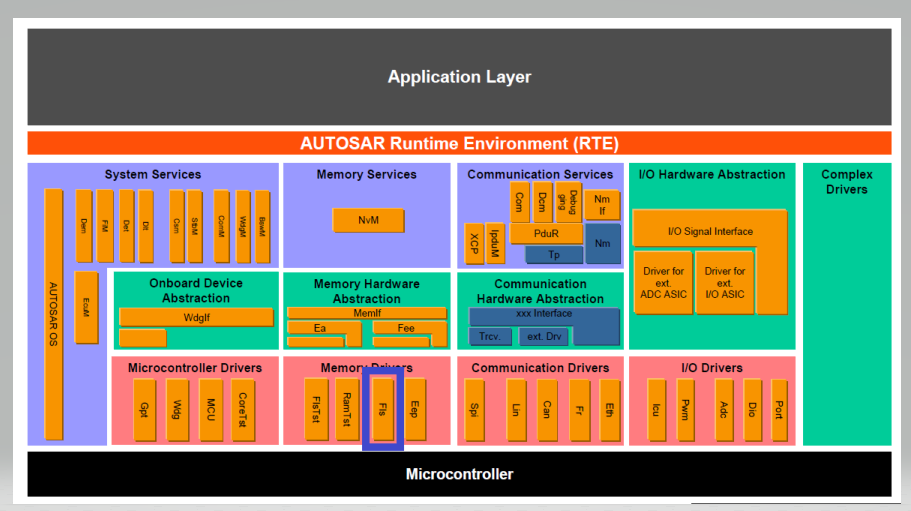
The figure below depicts the AUTOSAR layered architecture as 3 distinct layers,
The BSW is further divided into 4 layers:

MCAL is the lowest abstraction layer of the Basic Software. It contains internal drivers that are software modules that interact with the Microcontroller and its internal peripherals directly. Flash Driver is part of the Memory Drivers module, which is part of the Basic Software. The Flash Driver provides services for reading, writing, erasing flash memory and Execute-in-Place (XIP) mode for external Flash Device. The driver supports MT35XU512ABA1G12 and S28HS512T OSPI Flash Devices. The main tasks of the FLS driver are:
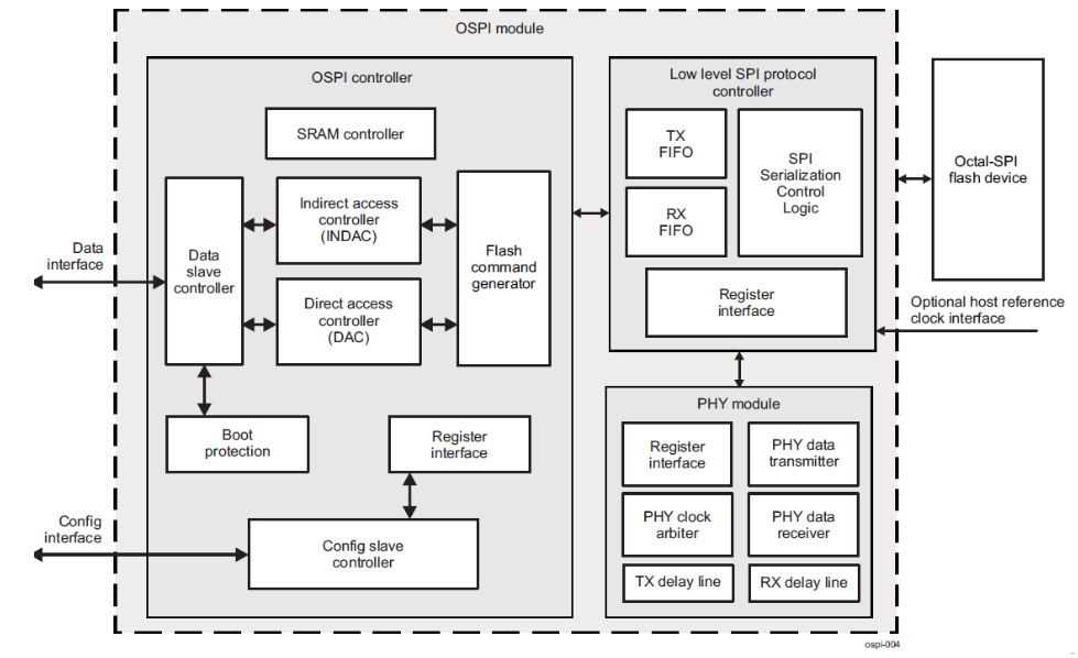
This Flash driver uses OSPI module to transfer data between the system and flash device. Below diagram shows the integration between the two hardware IPs that are used by the Flash Driver: FSS and OSPI. J721-EVM has one Flash device support - MT35XU512ABA1G12, and J7200-EVM has s28HS512T. Please note that this is for just reference purpose, for other details please refer to technical reference manual.
Diagrams are from device TRM.
Fls

The Flash Driver module includes the following main features:
| Sl No | Specification | Comment / Link |
|---|---|---|
| 1 | AUTOSAR 4.3.1 | AUTOSAR Specification for Flash Driver Internet Link |
| 2 | TDA4x TRM | Technical Reference Manual, TDA4X, FSS and OSPI module is detailed |
| 3 | BSW General Requirements / Coding guidelines | Intranet Link |
| 4 | Software Product Specification (SPS) | Intranet Link Requirements are derived from 1 |
The Flash Driver implements a standardized interface specified in the AUTOSAR_SWS_FlashDriver document, specified in: 4, 1 and 3. It’s recommended to refer 1 for clarification.

API features not supported
HW features not supported
Below listed points are assumed to be valid for this design/implementation, exceptions and other deviations are listed for each explicitly. Care should be taken to ensure these assumptions are addressed.
Fls module uses OSPI interface to transfer data between the system and the flash device. To be able to write to the flash, the flash has to be erased first. The erase operation internally programs 0xFF to all memory cells.
This Flash Driver Module Write, Read, Erase, BlankCheck and Compare APIs are asynchronous such that control will return to the application after the job from one of the APIs has been accepted. A "job" describes the action that will perform actual transactions to the hardware. The driver's Fls_MainFunction () API will do the job processing internally, after the APIs have been called and the job has been accepted. During job processing, the module will perform the programming of the flash device, and will make data transfers between system and flash device.
The Flash driver follows the code sequence outlined by the Autosar Spec for FLASH Module. Please refer to 1 for more details.
There are no hard requirements for resource allocation for Flash driver. Average Stack Size of FLS Driver is around 5 kilo bytes.
In terms of CPU load, there is not target defined for Flash Driver. We will measure and report this analysis post development.
For the Flash module instance, one interrupt service routine has been mapped. Note that Interrupt mode is only available when operating in INDAC mode. BlankCheck and Compare API are not functional with interrupt mode. The supported ISR is part of the Fls_Irq.h and Fls_Irq.c files.
Handling Flash OSPI FIFO Interrupt: OSPI Hardware Behavior: The hardware uses SRAM Watermark levels to trigger interrupts. There are two interrupts generated for every write/read call from SRAM to/from Flash memory. One interrupt notifies driver that the SRAM FIFO fill level is below a watermark level, which allows more data to be transferred into the SRAM. Another interrupt occurs when the transfer from SRAM into Flash memory, or to system memory, completes. Both these interrupts trigger the same ISR, and are handled accordingly within the ISR.
The Flash driver at any time will be in one of the following states. The state transition will depend on the APIs invoked by the application
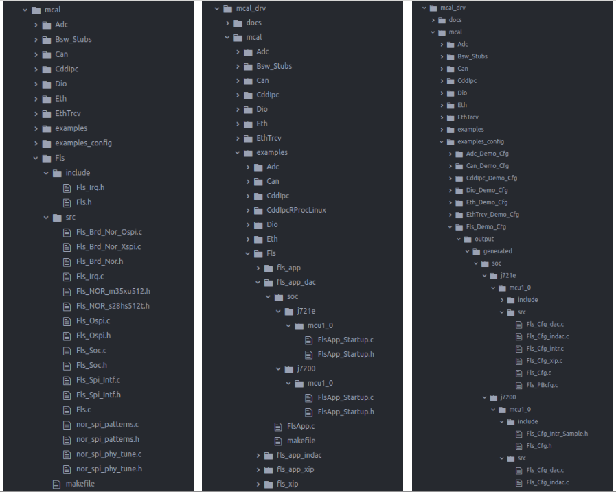
The diagram below shows the overall files structure for the Flash driver. The Fls.c and Fls.h are the 2 files that contain the Flash driver’s APIs.

Driver Implemented by
Example Application
| Design ID | DES_FLS_002 |
| Requirements Covered | MCAL-4169, MCAL-4179 |
The AUTOSAR Flash Driver Specification details mandatory parameters that shall be configurable via the configurator. Please refer section 10 1 Error Checks are common for variants of devices and we can do this in xdm or generator code.
| Design ID | DES_FLS_025 |
| Requirements Covered | MCAL-4821, MCAL-4820, MCAL-4819, MCAL-4818, MCAL-4824, MCAL-4822, MCAL-4416, MCAL-4415, MCAL-4414, MCAL-4413, MCAL-4412, MCAL-4411, MCAL-4408, MCAL-4406, MCAL-4404, MCAL-4403, MCAL-4398, MCAL-4396, MCAL-4395, MCAL-4394, MCAL-4391, MCAL-4390, MCAL-4388, MCAL-4387, MCAL-4386, MCAL-4384, MCAL-4383, MCAL-4381, MCAL-4380 |
The design's specific configurable parameters are as follows:
| Parameter | Usage comment |
|---|---|
| FlsDacEnable | Switch between INDAC and DAC mode. |
| FlsDtrEnable | Switch between DTR and STR mode. |
| FlsOspiClkSpeed | Clock Speed Freq Input (133MHz or 166MHz) |
| FlsXipEnable | Switch to turn on and off XIP mode. |
| FlsPhyEnable | Switch to turn on and off PHY mode. |
Please note that: The supported clock speeds are as follows:
The driver shall support both VARIANT-PRE-COMPILE & VARIANT-POST-BUILD.
Errors are classified in two categories, development error and Transient Faults.
The reported service IDs identify the services which are described earlier. The following table presents the service IDs and the related services:
| Service ID | Service |
| 0x00 | FLS_SID_INIT |
| 0x01 | FLS_SID_ERASE |
| 0x02 | FLS_SID_WRITE |
| 0x03 | FLS_SID_CANCEL |
| 0x04 | FLS_SID_GET_STATUS |
| 0x05 | FLS_SID_GET_JOB_RESULT |
| 0x06 | FLS_SID_MAIN_FUNCTION |
| 0x07 | FLS_SID_READ |
| 0x08 | FLS_SID_COMPARE |
| 0x09 | FLS_SID_SET_MODE |
| 0x10 | FLS_SID_GET_VERSION_INFO |
| 0x0A | FLS_SID_BLANK_CHECK |
AUTOSAR requires that API functions check the validity of their parameters and module status. The checks in table are internal parameter checks of the API functions. These checks are for development error reporting and can be enabled or disabled.
| Design ID | DES_FLS_006 |
| Requirements Covered | MCAL-4192, MCAL-4198, MCAL-4200, MCAL-4199, MCAL-4197, MCAL-4196, MCAL-4190, MCAL-4191, MCAL-4190 |
Development Error Reporting
The detection of development errors is configurable (ON / OFF) at pre-compile time. The switch FLS_DEV_ERROR_DETECT will activate or deactivate the detection of all development errors.
By default, development errors are reported to the DET using the service Det_ReportError(), if development error detection and reporting are enabled (i.e. checkboxes Development Mode and Development Error Reporting are checked).
| Type of Error | Related Error code | Value (Hex) |
| API service called with wrong parameter | FLS_E_PARAM_CONFIG | 0x01 |
| API service called with wrong parameter | FLS_E_PARAM_ADDRESS | 0x02 |
| API service called with wrong parameter | FLS_E_PARAM_LENGTH | 0x03 |
| API service called with wrong parameter | FLS_E_PARAM_DATA | 0x04 |
| API service used without module initialization | FLS_E_UNINIT | 0x05 |
| API called when module is busy | FLS_E_BUSY | 0x06 |
| API called with a Null Pointer | FLS_E_PARAM_POINTER | 0x0A |
Transient Faults
Transient errors are reported to the DET using the service Det_reportDetTransientFault(). The driver interface (Fls.h File Structure) lists the SID.
| Type of Error | Related Error code | Value (Hex) |
| Flash Erase Failed in HW | FLS_E_ERASE_FAILED | 0x01 |
| Flash Write Failed in HW | FLS_E_WRITE_FAILED | 0x02 |
| Flash Read Failed in HW | FLS_E_READ_FAILED | 0x03 |
| Flash Compare Failed in HW | FLS_E_COMPARE_FAILED | 0x04 |
| Expected HW ID not matched | FLS_E_UNEXPECTED_FLASH_ID | 0x05 |
Flash driver makes driver status available for debugging. The states MEMIF_UNINIT, MEMIF_IDLE, MEMIF_BUSY can be probed. Driver status variable is defined by the status element in the Fls_DrvObj.
The detailed API and interface description is available as part of 1 & 4. This section describes the API supported by the MCAL driver and the requirements covered by each of the API.
| Design ID | DES_FLS_009 |
| Requirements Covered | MCAL-4415, MCAL-4412, MCAL-4416, MCAL-4414, MCAL-4413, MCAL-4403, MCAL-4404, MCAL-4406, MCAL-4408, MCAL-4411, MCAL-4818, MCAL-4819, MCAL-4821, MCAL-4820, MCAL-4212 |
The sections below lists some of key data structures that shall be implemented and used in driver implementation.
| Macro | Comments |
|---|---|
| FLS_BASE_ADDRESS | Flash Memory start address, defines lower boundary for read/writ/erase/compare jobs. |
| FLS_TOTAL_SIZE | Total amount of flash memory in bytes. |
| FLS_DRIVER_INDEX | Index of driver, used by FEE - 0 for driver |
TypeDefs of address Type used by driver.
This type of the external data structure contains the initialization data for the Flash Driver, please refer section 8.2.1 of 1 Back To Top
This structure contain information about the Flash Device in use. For this driver design, and internal structure is used instead. Back To Top
For the standard APIs please refer 8.3 of 1. Sections below highlight other design considerations for the implementation.
Refer section 8.3.1 of 1
| Design ID | DES_FLS_010 |
| Requirements Covered | Requirements : MCAL-4217, MCAL-4224, MCAL-4222, MCAL-4219, MCAL-4223, MCAL-4220, MCAL-4221, MCAL-4218, MCAL-4191, MCAL-4190, MCAL-4192 |
Refer section 8.3.2 of 1
| Design ID | DES_FLS_011 |
| Requirements Covered | MCAL-4231, MCAL-4236, MCAL-4226, MCAL-4227, MCAL-4237, MCAL-4232, MCAL-4228, MCAL-4230, MCAL-4229, MCAL-4235. MCAL-4234, MCAL-4190, MCAL-4191, MCAL-4192 |
Refer section 8.3.3 of 1
| Design ID | DES_FLS_012 |
| Requirements Covered | MCAL-4244, MCAL-4239, MCAL-4249, MCAL-4250, MCAL-4243, MCAL-4242, MCAL-4245, MCAL-4251, MCAL-4248, MCAL-4247, MCAL-4190, MCAL-4191, MCAL-4192, MCAL-4241, MCAL_4252 |
Refer 8.3.5 of 1
| Design ID | DES_FLS_016 |
| Requirements Covered | MCAL-4262, MCAL-4391, MCAL-4263, MCAL-4264 |
Refer section 8.3.6 of 1
| Design ID | DES_FLS_013 |
| Requirements Covered | MCAL-4269, MCAL-4390, MCAL-4265, MCAL-4268, MCAL-4266, MCAL-4267, MCAL-4191 |
Refer section 8.3.7 of 1
| Design ID | DES_FLS_014 |
| Requirements Covered | MCAL-4275, MCAL-4280, MCAL-4270, MCAL-4271, MCAL-4281, MCAL-4272, MCAL-4274, MCAL-4273, MCAL-4283, MCAL-4279, MCAL-4278, MCAL-4282, MCAL-4190, MCAL-4191, MCAL-4192 |
Refer section 8.3.8 of 1
| Design ID | DES_FLS_015 |
| Requirements Covered | MCAL-4289, MCAL-4286, MCAL-4284, MCAL-4287, MCAL-4285, MCAL-4294, MCAL-4295, MCAL-4290, MCAL-4288, MCAL-4297, MCAL-4293, MCAL-4292, MCAL-4296, MCAL-4190, MCAL-4191, MCAL-4192 |
Refer section 8.3.10 of 1
| Design ID | DES_FLS_017 |
| Requirements Covered | MCAL-4302, MCAL-4303, MCAL-4190 |
Refer section 8.3.11 of 1
| Design ID | DES_FLS_018 |
| Requirements Covered | MMCAL-4309, MCAL-4306, MCAL-4384, MCAL-4304, MCAL-4314, MCAL-4315, MCAL-4308, MCAL-4310, MCAL-4307, MCAL-4312, MCAL-4190, MCAL-4191, MCAL-4192 |
Refer section 8.5.1 of 1
| Design ID | DES_FLS_019 |
| Requirements Covered | MCAL-4318, MCAL-4342, MCAL-4322, MCAL-4337, MCAL-4321, MCAL-4343, MCAL-4328, MCAL-4191 |
| Design ID | DES_FLS_020 |
| Requirements Covered | MCAL-4326, MCAL-4324, MCAL-4323, MCAL-4325, MCAL-4332, MCAL-4333, MCAL-4328, MCAL-4196, MCAL-4197, MCAL-4198, MCAL-4199, MCAL-4349, MCAL-4350, MCAL-4353 |
| Design ID | DES_FLS_021 |
| Requirements Covered | MCAL-4277, MCAL-4271 |
| Design ID | DES_FLS_022 |
| Requirements Covered | MCAL-4240, MCAL-4246 |
| Design ID | DES_FLS_023 |
| Requirements Covered | MCAL-4227, MCAL-4232, MCAL-4233 |
| Design ID | DES_FLS_024 |
| Requirements Covered | MCAL-4291, MCAL-4286 |
| Design ID | DES_FLS_025 |
| Requirements Covered | MCAL-4306, MCAL-4305, MCAL-4310, MCAL-4311 |
This design expects that implementation will require to use following global variables.
| Variable | Type | Description | Default Value |
|---|---|---|---|
| Fls_NorOspiInfo | Fls_NOR_InfoType | Flash Device Struct | - |
| Fls_DrvObj | Fls_DriverObjType | Flash driver object | - |
Sections below list some of the important design decisions and rational behind those decision.
The OSPI hardware module provides a couple ways to transfer data: DAC mode and INDAC mode.
CPU must have minimal restrictions while the flash driver is processing. Polling vs Interrupt mode should be allowed in the implementation.
DAC Mode
Direct Access Controller (or DAC) refers to the operation where data interface accesses directly trigger a read or write to Flash memory. It is memory mapped and can be used to both access and directly execute code from external Flash memory. Access that use DAC do not use the embedded SRAM within the OSPI module.
INDAC Mode
Indirect Access Controller (INDAC) uses the internal SRAM of the OSPI module. Data transfers then happen between the SRAM and Flash memory or SRAM and system memory, so no memory mapping is needed. The aim of the indirect mode of operation is to transfer significant numbers of bytes to/from Flash memory. Indirect operations are controlled and triggered by software via specific read/write transfer registers.
In case of a execute-in-place/memory mapped use case, DAC Poll mode should be used. Since DAC mode enables the PHY Module, it gives higher performance results for read operations. For better performance for write operations, INDAC Interrupt mode should be used.
The Flash device information should be available to the Flash Driver. Information such as Flash device sector size, number of sectors, page size, etc. is needed.
Avoid user input errors.
Use device specific, local structure
Only one Flash device is connected to the J7EVM, and this driver implementation only supported one device.
Use spec specific structure
Autosar Spec provide a specific structure that would come as input from user as a configuration parameter.
Option 1 is selected. The configuration parameter for FlsSector is not editable by the user, to avoid any error. Option 2 is useful when there are various flash devices connect, with varied size details. Since this Flash device contains sectors with all same sizes, Option 1 makes a simpler and more efficient design.
The Flash driver module needs to use SPI protocol to perform the data transfers between system and Flash device. Specifically, this Flash driver requires OSPI interface and driver.
SPI driver should have least impact on the latency and performance of the Flash driver.
Use PDK SPI Driver
TI's PDK package provides several different SPI drivers: OSPI, QSPI, NAND, or NOR. This driver could directly be used by MCAL Flash Driver.
Use MCAL SPI Driver
Autosar Spec specific MCAL SPI Driver is already present in MCUSW package.
Merge OSPI Driver
The required OSPI driver API and functions can be implemented inside the Flash driver itself. Therefore, the OSPI driver would be part of the Flash Driver module.
Option 3 is selected as it reduces the latency and would give better performance. Also, this option decreases the dependency on other modules and packages.
The sections below identify some of the aspects of design that would require emphasis during testing of this design implementation
| Revision | Date | Author | Description | Status |
|---|---|---|---|---|
| 0.1 | 26 May 2020 | Nikki Shah | First version | Pending |
| 0.1 | 01 June 2020 | Nikki Shah | Addressed Review Comments | Approved |
| 0.2 | 02 Nov 2020 | Nikki Shah | MCUSW 01_03_00 Release Updates | Pending |
 1.8.15