
5.12. CDD CMPSS Module
5.12.1. Acronyms and Definitions
Abbreviation/Term |
Explanation |
|---|---|
AUTOSAR |
Automotive Open System Architecture |
CDD |
Complex Device Driver |
CMPSS |
Comparator Subsystem |
DAC |
Digital-to-Analog Converter |
DE |
Diode Emulation |
API |
Application Programming Interface |
DET |
Default Error Tracer |
ADC |
Analog-to-Digital Converter |
EPWM |
Enhanced Pulse Width Modulator |
HYS |
Hysteresis |
LSB |
Least Significant Bit |
SEU |
Single Event Upset |
TRM |
Technical Reference Manual |
VDAC |
DAC Reference Voltage |
HW |
Hardware |
SW |
Software |
5.12.2. Introduction
The CDD CMPSS driver is a Complex Device Driver for the Comparator Subsystem, an analog comparator peripheral used to monitor analog signals against a programmable threshold and generate trip signals for protection and control applications (for example, over-current or over-voltage trip of EPWM outputs).
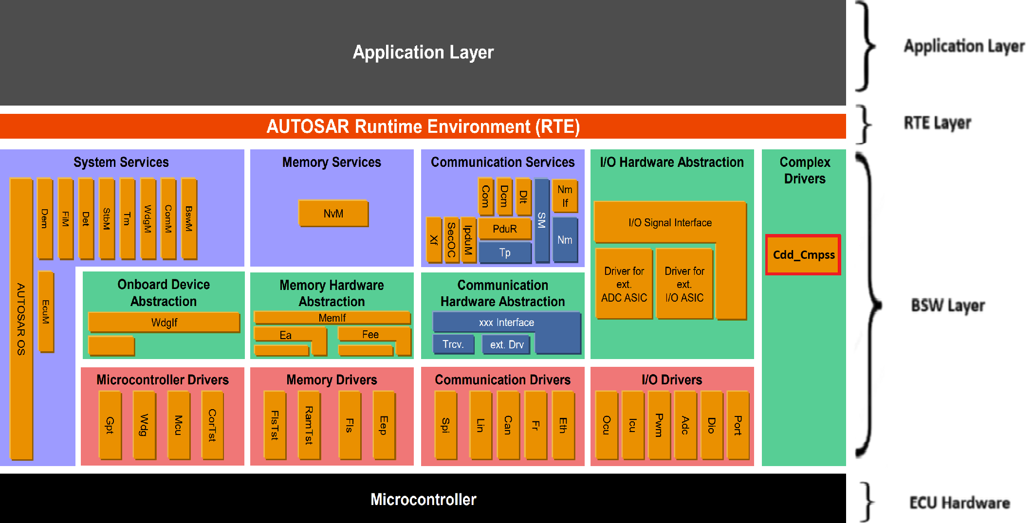
Fig. 5.62 Cdd Cmpss MCAL AUTOSAR
This document details AUTOSAR Cdd CMPSS module implementation
Supported AUTOSAR Release |
4.3.1 |
|---|---|
Supported Configuration Variants |
Pre-Compile |
Vendor ID |
CDD_CMPSS_VENDOR_ID (44) |
Module ID |
CDD_CMPSS_MODULE_ID (255) |
5.12.3. Functional Overview
The CDD CMPSS driver is part of the Complex Device Driver layer (CDD). Each CMPSS hardware instance contains a High comparator and a Low comparator, an independently programmable 12-bit reference DAC per side, a ramp generator per side, and a digital filter per side. The driver exposes both a one-time integration-time configuration surface (comparator source, DAC, ramp, filter, output routing) and a runtime reconfiguration surface that lets an integrator adjust thresholds, hysteresis, filtering, and ramp parameters after Cdd_Cmpss_Init() without re-initializing the whole module.
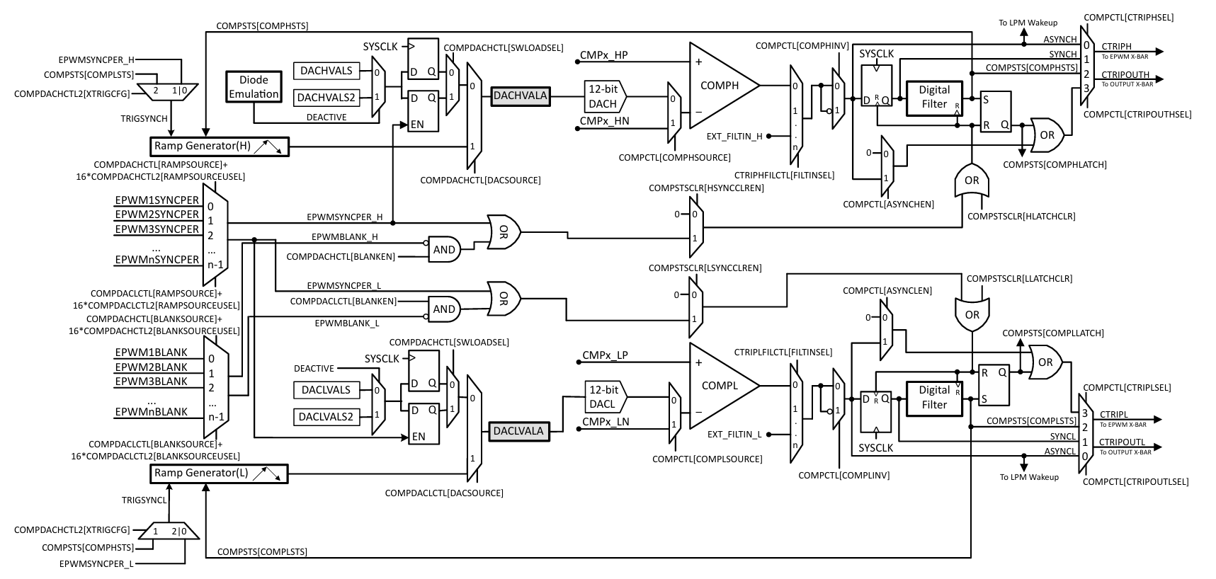
Fig. 5.63 Cdd_Cmpss Block Diagram
5.12.3.1. Initialization
Cdd_Cmpss_Init() takes a pointer to a Cdd_Cmpss_ConfigType structure containing an array of per-instance configurations (Cdd_Cmpss_HwInstanceCfgType) and validates and applies every configured instance’s comparator, DAC, ramp, filter, and output-routing settings in one call. Cdd_Cmpss_DeInit() clears the COMPDACE enable bit on every configured instance and clears the internal initialized flag.
Only the Pre-Compile configuration variant is supported. In this variant, Cdd_Cmpss_Init() must be called with NULL_PTR — the driver then loads the configuration generated at build time into Cdd_Cmpss_Cfg.c from the EB Tresos configuration. Passing any other pointer value in this variant is rejected as CDD_CMPSS_E_PARAM_POINTER, since the Pre-Compile build path only recognizes the NULL_PTR convention. The loaded configuration is not modifiable at runtime, other than through the runtime Config*()/Set*() API described below.
5.12.3.2. States
The driver tracks two logical states, UNINIT and INIT, through an internal Cdd_Cmpss_IsInitialized flag rather than a full AUTOSAR state machine. Cdd_Cmpss_Init() transitions UNINIT to INIT; Cdd_Cmpss_DeInit() transitions INIT back to UNINIT. Every other API (other than Cdd_Cmpss_Init() and, where applicable, Cdd_Cmpss_GetVersionInfo()) requires the driver to already be in the INIT state — this is enforced centrally by an internal Cdd_Cmpss_ValidateInitAndInstanceId() helper, which raises CDD_CMPSS_E_UNINIT otherwise.
5.12.3.3. Assumptions
The CMPSS hardware instance(s) used by the application have been allocated, and their base address, frame, debug/standby behavior, and comparator input pin multiplexing have been configured, through the Resource Allocator before
Cdd_Cmpss_Init()is called.The MCU clocks required by the CMPSS peripheral instance(s) in use are enabled before
Cdd_Cmpss_Init()is called.Once
Cdd_Cmpss_ApplyLock()has been called for a given register group, the integrator does not attempt further runtime reconfiguration of that group; the driver does not detect, and cannot report, a write that hardware silently discards because the group is locked.
5.12.3.4. Limitations
Cdd_Cmpss_ApplyLock()is irreversible on a per-bit basis until the next device reset. There is no runtime API to clear COMPLOCK.A
Config*()/Set*()call made after the corresponding register group has been locked returnsE_OK(assuming its own parameter validation passes) even though hardware silently discards the write; the driver performs no post-write readback and raises no DET error for this case.Cdd_Cmpss_RampCfgType.Enable(CddCmpssHighRampEnable/CddCmpssLowRampEnablein the Tresos configuration) is not read by the driver at runtime. Whether a ramp generator drives its DAC is controlled entirely by that side’sDacSourcesetting; theEnablefield only gates whether the rest of that side’s ramp parameters are editable in the Tresos GUI.Cdd_Cmpss_ConfigDEActiveSource()does not range-checkSource: the enum ordinal is written directly to the 5-bitDEACTIVESELfield with no DET validation.Cdd_Cmpss_ConfigFilter()only writes the digital filter’s sample-window/threshold/input-select registers; it does not itself apply them. Without a followingCdd_Cmpss_InitFilter()call, the filter keeps running with its previous configuration.
5.12.3.5. Design Overview
The driver is split into a public API layer (Cdd_Cmpss.c) and a private register-access helper layer (Cdd_Cmpss_Priv.c). Each configured instance is described by a Cdd_Cmpss_HwInstanceCfgType structure containing module-level fields that apply to the whole instance — DacRef (voltage reference for BOTH DACs: internal VDDA or external VDAC_REF pin — physically a field in the High DAC’s control register, but the Low DAC has no reference-select of its own), SwLoadSel (shadow-to-active load trigger for BOTH DAC shadow registers: next SYSCLK cycle or EPWMnSYNCPER event), FreeSoft (ramp behavior for BOTH ramp generators during an emulation halt: stop, run-to-zero, or free-run), XtrigCfg (ramp cross-triggering between the High and Low ramps), and DeModeCfg (Diode Emulation enable and DEACTIVE source select for BOTH DACs) — together with a pair of per-side (CDD_CMPSS_SIDE_HIGH / CDD_CMPSS_SIDE_LOW) sub-configurations covering the comparator, DAC, ramp, and filter for that side.
At runtime, most API functions take an InstanceId (a plain uint8, using the Tresos-generated Cdd_CmpssConf_CddCmpssHwInstance_<name> symbolic constant for the target instance) and, where the operation is side-specific, a Cdd_Cmpss_CompSideType (CDD_CMPSS_SIDE_HIGH / CDD_CMPSS_SIDE_LOW). Unlike an opaque handle, InstanceId is used directly as an index into the configuration array and is bounds-checked against CDD_CMPSS_HW_INSTANCE_COUNT; an out-of-range value is rejected as CDD_CMPSS_E_PARAM_VALUE.
5.12.4. Hardware Features
5.12.4.1. Hardware Features Supported
Up to twelve independent CMPSS hardware instances (CMPSS1–CMPSS12), each with a High comparator and a Low comparator
Two independently programmable 12-bit reference DACs per instance (High DAC, Low DAC), each selectable to drive either a static shadow value or the output of a ramp generator
Comparator negative input independently selectable per side between the internal reference DAC and an external pin (
CDD_CMPSS_COMP_SOURCE_DAC/CDD_CMPSS_COMP_SOURCE_PIN)Programmable hysteresis, common to both sides, to prevent trip chatter when the input signal is noisy near the threshold — five levels (
CDD_CMPSS_HYS_NONEthroughCDD_CMPSS_HYS_4X, approximately 12 LSB per step)Two independent ramp generators (High and Low), each with programmable direction (increment/decrement), reference value, step value, delay, and clock divider (shadow and active register pairs), EPWM-synchronized reload, and configurable reload source on a comparator trip event
Ramp cross-triggering to keep the High and Low ramps in a fixed phase relationship without extra EPWM wiring: independent, Low-triggered-by-High-end-of-ramp, or High-triggered-by-Low-end-of-ramp
Two digital majority-vote filters per instance (one per side), with configurable sample window and vote threshold, and a dedicated filter-initialization sequence (
Cdd_Cmpss_InitFilter()) that must complete before the filtered/latched trip-output source is selectedTrip output routing selectable per side among asynchronous, synchronous, filtered, and latched-filter sources
Automatic latch clear on
EPWMnSYNCPER(Cdd_Cmpss_ConfigSyncClear()) as an alternative to explicitCdd_Cmpss_ClearLatch()callsBlanking window support to mask trip signals during a configurable EPWM-synchronized window, so a known switching transient (e.g. right after a PWM output turns on) does not register as a false trip
Diode Emulation (DE) mode: automatically switches BOTH the High and Low comparator thresholds between two DAC values in step with a shared EPWM DEACTIVE signal, emulating the trip-point behavior of a free-wheeling diode in a synchronous-rectifier power stage without an actual diode
Permanent configuration lock (
Cdd_Cmpss_ApplyLock(), backed by the COMPLOCK register) that freezes one or more of four independent register groups — comparator control, hysteresis control, DAC/ramp control, and filter/trip control — against further runtime changes until the next device reset
5.12.4.2. Not supported Features
None
5.12.4.3. Non compliance
None
5.12.5. Source files
📦f29h85x_mcal
┣ 📂build
┣ 📂docs
┣ 📂drivers
┃ ┣ 📂BSW_Stubs
┃ ┣ 📂Adc
┃ ┣ 📂Can
┃ ┣ 📂Cdd_Cmpss
┃ ┃ ┣ 📂include
┃ ┃ ┃ ┣ 📜Cdd_Cmpss.h : Contains the API declarations of the Cdd CMPSS driver to be used by upper layers.
┃ ┃ ┃ ┗ 📜Cdd_Cmpss_Priv.h : Contains data structures and Internal function declarations.
┃ ┃ ┣ 📂src
┃ ┃ ┃ ┣ 📜Cdd_Cmpss.c : Contains the implementation of the API for Cdd CMPSS driver.
┃ ┃ ┃ ┗ 📜Cdd_Cmpss_Priv.c : Contains Functions that support the API for Cdd CMPSS driver
┃ ┃ ┗ 📜CMakeLists.txt
┃ ┣ 📂Cdd_Dma
┃ ┣ 📂Dio
┃ ┣ 📂Gpt
┃ ┣ 📂hw_include
┃ ┣ 📂Mcal_Lib
┃ ┣ 📂Mcu
┃ ┣ 📂Port
┃ ┣ 📂Spi
┃ ┗ 📂Wdg
┣ 📂examples
┣ 📂plugins
┣ 📜CMakeLists.txt
┗ 📜CMakePresets.json
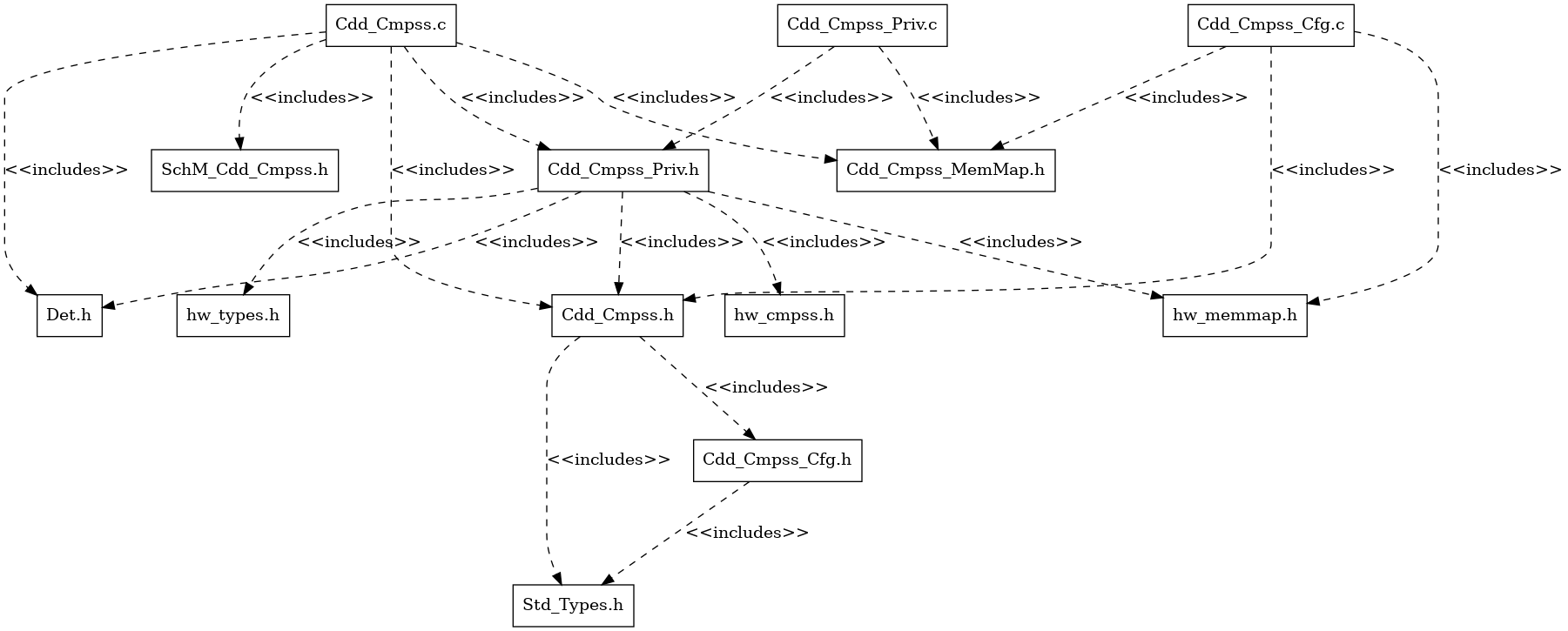
Fig. 5.64 Cdd Cmpss Header File Structure
5.12.6. Module requirements
5.12.6.1. Memory Mapping
The driver follows the AUTOSAR memory mapping strategy. All memory sections should be stored in memory as per AUTOSAR specifications, considering initialization policy, alignment requirements, safety classification, and core scope where applicable.
Reference memory map files can be found at:
{MCAL_INSTALL_PATH}\drivers\BSW_Stubs\MemMap\include
The memory sections are organized according to AUTOSAR specifications to ensure proper placement of code and data in different memory regions based on their usage and access patterns.
5.12.6.2. Scheduling
None
5.12.6.3. Error handling
5.12.6.3.1. Development Error Reporting
Development errors are reported to the DET using the service Det_ReportError(), when enabled. The driver interface contains the MACRO declaration of the error codes to be returned.
5.12.6.4. Error codes
Type of Error |
Related Error code |
Value (Hex) |
|---|---|---|
API service used without module initialization |
CDD_CMPSS_E_UNINIT |
0x00 |
API called for reinitialization of an already initialized CMPSS driver |
CDD_CMPSS_E_ALREADY_INITIALIZED |
0x01 |
API service called with an invalid parameter pointer |
CDD_CMPSS_E_PARAM_POINTER |
0x02 |
API service called with an out-of-range parameter value, including an |
CDD_CMPSS_E_PARAM_VALUE |
0x04 |
API service called with an invalid Side parameter |
CDD_CMPSS_E_PARAM_SIDE |
0x05 |
5.12.7. Used resources
5.12.7.1. Interrupt Handling
None. This driver does not register or require any interrupt service routines of its own. Comparator trip and filter/latch status are read directly through Cdd_Cmpss_GetStatus() or are consumed by downstream peripherals (EPWM trip-zone inputs, X-Bar routing); any interrupt behavior associated with a trip event, such as an EPWM trip-zone interrupt, is owned and documented by the consuming module (see the Cdd_Pwm Module User Guide), not by Cdd_Cmpss.
5.12.7.2. Instance support
CPU instances |
supported |
|---|---|
CPU 1 |
YES |
CPU 2 |
Not exercised by any current reference example or Resource Allocator configuration |
CPU 3 |
Not exercised by any current reference example or Resource Allocator configuration |
5.12.7.3. Hardware-Software Mapping
Below image shows Cdd CMPSS driver Hardware-Software mapping. For more information related to HW/SW mapping, refer the F29x Reference Manual.
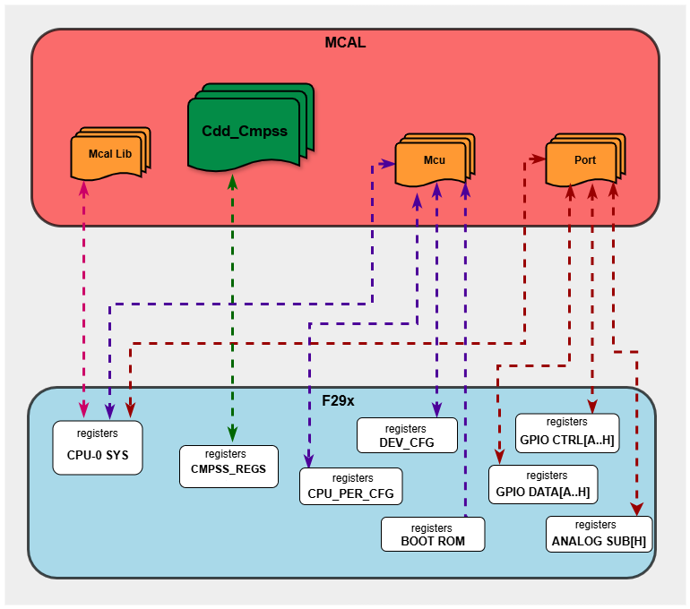
Fig. 5.65 Cdd CMPSS HW/SW Mapping
5.12.8. Integration description
5.12.8.1. Dependent modules
5.12.8.1.1. DET
This implementation depends on the DET in order to report development errors. The detection of development errors is configurable (ON / OFF). The switch CDD_CMPSS_DEV_ERROR_DETECT will activate or deactivate the detection of all development errors.
5.12.8.1.2. MCU
MCU Module is required to initialize all the clocks to be used by different peripherals including the CMPSS module.
5.12.8.1.3. SchM
If multiple AUTOSAR runnables have access to the same Data Store Memory block, the exported AUTOSAR specification enforces data consistency by using an AUTOSAR exclusive area. With this specification, the runnables have mutually exclusive access to the per-instance memory global data, which prevents data corruption. Beside the OS, the BSW Scheduler provides functions that Cdd_Cmpss module calls at begin and end of critical sections. This implementation requires 1 level of exclusive access to guard critical sections.
The data consistency mechanism that has to be applied to an ExclusiveArea might be domain, ECU or even project specific. The decision which mechanism has to be applied by RTE / Basic Software Scheduler is taken during ECU integration by setting the Exclusive Area configuration parameter RteExclusiveAreaImplMechanism. This parameter is an input for RTE generator.
For CDD_CMPSS Module, data consistency and exclusive access to critical sections are required for the following sections as shown in the table below:
Exclusive Area Functions used |
Cdd_Cmpss Function calling Exclusive Area |
Need for Exclusive Area |
Recommended Exclusive Area Mapping |
|---|---|---|---|
CDD_CMPSS_EXCLUSIVE_AREA_0 |
Cdd_Cmpss_SetModuleEnable |
To protect against multiple access for shared resources |
ALL_INTERRUPT_BLOCKING : All interrupts should be blocked as this API’s can be called in the interrupts. |
5.12.8.2. Resource Allocator
The CDD CMPSS module uses the Resource Allocator to allocate CMPSS peripheral instances to a CPU context and configure their memory-mapped base addresses, debug/standby behavior, and comparator input pin multiplexing. Each allocation is placed inside a Context that maps to a CPU core (e.g. CPU1). See the Resource Allocator Module User Guide for details on configuring device-specific settings.
5.12.8.2.1. Resource Allocator Usage Example
To allocate CMPSS1 to CPU1:
In the Resource Allocator configuration, navigate to the desired Context (e.g. CPU1_Context) and, under
Context/Cdd_Cmpss, create a newCdd_CmpssAllocatedInstance.Set InstanceName to the physical instance to allocate (
CMPSS1–CMPSS12).Set Frame (
FRAME0–FRAME3). The BaseAddr is auto-calculated from the selected instance and frame.Set DebugHaltEnabled and StandbyModeEnabled according to the desired debug/low-power behavior.
Set CMPSSHPMuxSelect and CMPSSLPMuxSelect to the pin (or internal signal) actually wired to the High-side and Low-side positive comparator inputs.
Set CMPSSHNMuxSelect and CMPSSLNMuxSelect to the pin actually wired to the High-side and Low-side negative comparator inputs. These only matter when
Cdd_Cmpss_ConfigComparator()selectsCDD_CMPSS_COMP_SOURCE_PINfor that side; when the internal DAC drives the negative input (CDD_CMPSS_COMP_SOURCE_DAC), these selections are unused.
ResourceAllocatorGeneral
└── Context (Core: CPU1)
    └── Cdd_Cmpss
        └── Cdd_CmpssAllocatedInstance
            ├── InstanceName: CMPSS1
            ├── Frame: FRAME0
            ├── BaseAddr: CMPSS1_BASE_FRAME(0U)  [auto-calculated]
            ├── DebugHaltEnabled: true
            ├── StandbyModeEnabled: true
            ├── CMPSSHPMuxSelect / CMPSSLPMuxSelect
            └── CMPSSHNMuxSelect / CMPSSLNMuxSelect
Note
Unlike some other CDD modules on this device, CMPSS instance allocation is a single-level configuration performed directly under the CPU context — there is no separate CPU1-only global configuration level for CMPSS.
5.12.9. Safety Mechanism
TI Diagnostic Unique Identifier |
Summary |
Description |
|---|---|---|
CMPSS2 |
LOCK Mechanism for Control Registers |
|
Note
More details of Safety Mechanisms can be found in Safety Manual.
5.12.10. Configuration
The Cdd CMPSS Driver implementation supports single configuration variants, namely Pre-Compile config. The driver expects generated Cdd_Cmpss_Cfg.h to be present as input file. The associated Cdd CMPSS driver configuration generated source file is Cdd_Cmpss_Cfg.c.
The generated configuration files should not be modified manually. The config tool Elektrobit Tresos should be used to modify the configuration files.
Note
Refer section Getting Started with EB Tresos of Chapter MCAL Configuration and EB Tresos for more information on how to load plugin and generate the configuration files.
5.12.10.1. Configuration Parameters
5.12.10.1.1. CddCmpssGeneral
General configuration parameters for the CDD_CMPSS driver.
5.12.10.1.1.1. CddCmpssDevErrorDetect
Item |
|
|---|---|
Name |
CddCmpssDevErrorDetect |
Description |
Enable/disable Development Error Detection via DET. |
Origin |
Texas Instruments |
Post-Build-Variant-Value |
false |
Value-Configuration-Class |
– |
Pre-Compile-Time |
VARIANT-PRE-COMPILE |
Default-value |
true |
5.12.10.1.1.2. CddCmpssGetVersionInfoApi
Item |
|
|---|---|
Name |
CddCmpssGetVersionInfoApi |
Description |
Enable/disable the Cdd_Cmpss_GetVersionInfo() API. |
Origin |
Texas Instruments |
Post-Build-Variant-Value |
false |
Value-Configuration-Class |
– |
Pre-Compile-Time |
VARIANT-PRE-COMPILE |
Default-value |
true |
5.12.10.1.2. CddCmpssConfigSet
Top-level configuration set container.
5.12.10.1.2.1. CddCmpssHwInstance
Per-instance CMPSS hardware configuration.
5.12.10.1.2.2. CddCmpssHwUnit
Item |
|
|---|---|
Name |
CddCmpssHwUnit |
Description |
Physical CMPSS hardware unit - derived from the InstanceName of CddCmpssHwInstanceRef (read-only). |
Origin |
Texas Instruments |
Post-Build-Variant-Value |
false |
Value-Configuration-Class |
– |
Pre-Compile-Time |
VARIANT-PRE-COMPILE |
Default-value |
CDD_CMPSS_HW_UNIT_1 |
Range |
CDD_CMPSS_HW_UNIT_1 |
5.12.10.1.2.3. CddCmpssHPMuxSelect
Item |
|
|---|---|
Name |
CddCmpssHPMuxSelect |
Description |
HP positive input mux select - read from ResourceAllocator CddCmpssHwInstanceRef/CMPSSHPMuxSelect (read-only). |
Origin |
Texas Instruments |
Post-Build-Variant-Value |
false |
Value-Configuration-Class |
– |
Pre-Compile-Time |
VARIANT-PRE-COMPILE |
Default-value |
CMPSS_INPUT_SIGNAL_MUX0_AIO160 |
Range |
CMPSS_INPUT_SIGNAL_MUX0_AIO160 |
5.12.10.1.2.4. CddCmpssLPMuxSelect
Item |
|
|---|---|
Name |
CddCmpssLPMuxSelect |
Description |
LP positive input mux select - read from ResourceAllocator CddCmpssHwInstanceRef/CMPSSLPMuxSelect (read-only). |
Origin |
Texas Instruments |
Post-Build-Variant-Value |
false |
Value-Configuration-Class |
– |
Pre-Compile-Time |
VARIANT-PRE-COMPILE |
Default-value |
CMPSS_INPUT_SIGNAL_MUX0_AIO160 |
Range |
CMPSS_INPUT_SIGNAL_MUX0_AIO160 |
5.12.10.1.2.5. CddCmpssHNMuxSelect
Item |
|
|---|---|
Name |
CddCmpssHNMuxSelect |
Description |
HN negative input mux select - read from ResourceAllocator CddCmpssHwInstanceRef/CMPSSHNMuxSelect (read-only). |
Origin |
Texas Instruments |
Post-Build-Variant-Value |
false |
Value-Configuration-Class |
– |
Pre-Compile-Time |
VARIANT-PRE-COMPILE |
Default-value |
CMPSS_NEG_INPUT_SIGNAL_MUX0_AIO161 |
Range |
CMPSS_NEG_INPUT_SIGNAL_MUX0_AIO161 |
5.12.10.1.2.6. CddCmpssLNMuxSelect
Item |
|
|---|---|
Name |
CddCmpssLNMuxSelect |
Description |
LN negative input mux select - read from ResourceAllocator CddCmpssHwInstanceRef/CMPSSLNMuxSelect (read-only). |
Origin |
Texas Instruments |
Post-Build-Variant-Value |
false |
Value-Configuration-Class |
– |
Pre-Compile-Time |
VARIANT-PRE-COMPILE |
Default-value |
CMPSS_NEG_INPUT_SIGNAL_MUX0_AIO161 |
Range |
CMPSS_NEG_INPUT_SIGNAL_MUX0_AIO161 |
5.12.10.1.2.7. CddCmpssHysteresis
Item |
|
|---|---|
Name |
CddCmpssHysteresis |
Description |
Dead-band around the DAC threshold to prevent chatter when the input signal is noisy near the trip point. Applies to both comparators.
|
Origin |
Texas Instruments |
Post-Build-Variant-Value |
false |
Value-Configuration-Class |
– |
Pre-Compile-Time |
VARIANT-PRE-COMPILE |
Default-value |
CDD_CMPSS_HYS_NONE |
Range |
CDD_CMPSS_HYS_NONE |
5.12.10.1.2.8. CddCmpssXtrigCfg
Item |
|
|---|---|
Name |
CddCmpssXtrigCfg |
Description |
Cross-trigger coupling between the High-side and Low-side ramp generators.
|
Origin |
Texas Instruments |
Post-Build-Variant-Value |
false |
Value-Configuration-Class |
– |
Pre-Compile-Time |
VARIANT-PRE-COMPILE |
Default-value |
CDD_CMPSS_XTRIG_INDEPENDENT |
Range |
CDD_CMPSS_XTRIG_INDEPENDENT |
5.12.10.1.2.9. CddCmpssHwInstanceRef
Item |
|
|---|---|
Name |
CddCmpssHwInstanceRef |
Description |
Reference to the CMPSS instance allocated in the ResourceAllocator. Provides the base address used by the driver. |
Origin |
Texas Instruments |
Post-Build-Variant-Value |
false |
Value-Configuration-Class |
– |
Pre-Compile-Time |
VARIANT-PRE-COMPILE |
5.12.10.1.2.10. CddCmpssHighCompCfg
High comparator input source, output inversion, trip routing and async path (single-side).
5.12.10.1.2.11. CddCmpssSource
Item |
|
|---|---|
Name |
CddCmpssSource |
Description |
Selects what feeds the High comparator’s negative input: the internal reference DAC (for a programmable threshold) or the external pin CMPIN1H (for a threshold driven by another device, e.g. another DAC). |
Origin |
Texas Instruments |
Post-Build-Variant-Value |
false |
Value-Configuration-Class |
– |
Pre-Compile-Time |
VARIANT-PRE-COMPILE |
Default-value |
CDD_CMPSS_COMP_SOURCE_DAC |
Range |
CDD_CMPSS_COMP_SOURCE_DAC |
5.12.10.1.2.12. CddCmpssInvert
Item |
|
|---|---|
Name |
CddCmpssInvert |
Description |
Inverts the High comparator’s trip sense so it fires when the input signal falls below the threshold instead of when it rises above it. Use when the condition being monitored is active-low (e.g. a fault signal that is normally high and goes low to indicate a trip). |
Origin |
Texas Instruments |
Post-Build-Variant-Value |
false |
Value-Configuration-Class |
– |
Pre-Compile-Time |
VARIANT-PRE-COMPILE |
Default-value |
false |
5.12.10.1.2.13. CddCmpssAsyncEn
Item |
|
|---|---|
Name |
CddCmpssAsyncEn |
Description |
ORs the High comparator’s raw async output into the latched-filter trip path for the fastest possible trip response. Only takes effect if this side’s CtripSel or CtripoutSel below is set to the Latched filter output option - otherwise this bit is a hardware no-op (the driver DET-rejects that combination). Enable for time-critical protection trips (e.g. over-current shutoff) together with Latched routing; leave disabled to use the synchronized or filtered path on its own, which is easier to reason about in timing analysis. |
Origin |
Texas Instruments |
Post-Build-Variant-Value |
false |
Value-Configuration-Class |
– |
Pre-Compile-Time |
VARIANT-PRE-COMPILE |
Default-value |
false |
5.12.10.1.2.14. CddCmpssLowCompCfg
Low comparator input source, output inversion, trip routing and async path (single-side).
5.12.10.1.2.15. CddCmpssSource
Item |
|
|---|---|
Name |
CddCmpssSource |
Description |
Selects what feeds the Low comparator’s negative input: the internal reference DAC (for a programmable threshold) or the external pin CMPIN1L (for a threshold driven by another device, e.g. another DAC). |
Origin |
Texas Instruments |
Post-Build-Variant-Value |
false |
Value-Configuration-Class |
– |
Pre-Compile-Time |
VARIANT-PRE-COMPILE |
Default-value |
CDD_CMPSS_COMP_SOURCE_DAC |
Range |
CDD_CMPSS_COMP_SOURCE_DAC |
5.12.10.1.2.16. CddCmpssInvert
Item |
|
|---|---|
Name |
CddCmpssInvert |
Description |
Inverts the Low comparator’s trip sense so it fires when the input signal falls below the threshold instead of when it rises above it. Use when the condition being monitored is active-low (e.g. a fault signal that is normally high and goes low to indicate a trip). |
Origin |
Texas Instruments |
Post-Build-Variant-Value |
false |
Value-Configuration-Class |
– |
Pre-Compile-Time |
VARIANT-PRE-COMPILE |
Default-value |
false |
5.12.10.1.2.17. CddCmpssAsyncEn
Item |
|
|---|---|
Name |
CddCmpssAsyncEn |
Description |
ORs the Low comparator’s raw async output into the latched-filter trip path for the fastest possible trip response. Only takes effect if this side’s CtripSel or CtripoutSel below is set to the Latched filter output option - otherwise this bit is a hardware no-op (the driver DET-rejects that combination). Enable for time-critical protection trips (e.g. over-current shutoff) together with Latched routing; leave disabled to use the synchronized or filtered path on its own, which is easier to reason about in timing analysis. |
Origin |
Texas Instruments |
Post-Build-Variant-Value |
false |
Value-Configuration-Class |
– |
Pre-Compile-Time |
VARIANT-PRE-COMPILE |
Default-value |
false |
5.12.10.1.2.18. CddCmpssHighOutputCfg
Selects which processed version of the High comparator’s output is presented as its trip signal, both internally (CTRIPH) and on the output crossbar (CTRIPOUTH). If either is set to use the digital filter, configure and initialize the filter first (Cdd_Cmpss_InitFilter()) - selecting a filtered source before the filter has been initialized presents undefined filter output.
5.12.10.1.2.19. CddCmpssCtripSel
Item |
|
|---|---|
Name |
CddCmpssCtripSel |
Description |
Signal stage that feeds the High comparator’s internal trip output (CTRIPH), used by on-chip peripherals such as EPWM trip zones.
|
Origin |
Texas Instruments |
Post-Build-Variant-Value |
false |
Value-Configuration-Class |
– |
Pre-Compile-Time |
VARIANT-PRE-COMPILE |
Default-value |
CDD_CMPSS_TRIP_SEL_ASYNC |
Range |
CDD_CMPSS_TRIP_SEL_ASYNC |
5.12.10.1.2.20. CddCmpssCtripoutSel
Item |
|
|---|---|
Name |
CddCmpssCtripoutSel |
Description |
Signal stage that feeds the High comparator’s output-crossbar trip signal (CTRIPOUTH), used to route the trip to other peripherals or an output pin through the X-BAR. Same four choices as CtripSel ? ASYNC, SYNC, FILTER, LATCHED (see CtripSel for definitions). CtripSel and CtripoutSel are independent, e.g. ASYNC internally for lowest latency while FILTER is exposed externally. |
Origin |
Texas Instruments |
Post-Build-Variant-Value |
false |
Value-Configuration-Class |
– |
Pre-Compile-Time |
VARIANT-PRE-COMPILE |
Default-value |
CDD_CMPSS_TRIP_SEL_ASYNC |
Range |
CDD_CMPSS_TRIP_SEL_ASYNC |
5.12.10.1.2.21. CddCmpssLowOutputCfg
Selects which processed version of the Low comparator’s output is presented as its trip signal, both internally (CTRIPL) and on the output crossbar (CTRIPOUTL). If either is set to use the digital filter, configure and initialize the filter first (Cdd_Cmpss_InitFilter()) - selecting a filtered source before the filter has been initialized presents undefined filter output.
5.12.10.1.2.22. CddCmpssCtripSel
Item |
|
|---|---|
Name |
CddCmpssCtripSel |
Description |
Signal stage that feeds the Low comparator’s internal trip output (CTRIPL), used by on-chip peripherals such as EPWM trip zones.
|
Origin |
Texas Instruments |
Post-Build-Variant-Value |
false |
Value-Configuration-Class |
– |
Pre-Compile-Time |
VARIANT-PRE-COMPILE |
Default-value |
CDD_CMPSS_TRIP_SEL_ASYNC |
Range |
CDD_CMPSS_TRIP_SEL_ASYNC |
5.12.10.1.2.23. CddCmpssCtripoutSel
Item |
|
|---|---|
Name |
CddCmpssCtripoutSel |
Description |
Signal stage that feeds the Low comparator’s output-crossbar trip signal (CTRIPOUTL), used to route the trip to other peripherals or an output pin through the X-BAR. Same four choices as CtripSel ? ASYNC, SYNC, FILTER, LATCHED (see CtripSel for definitions). CtripSel and CtripoutSel are independent, e.g. ASYNC internally for lowest latency while FILTER is exposed externally. |
Origin |
Texas Instruments |
Post-Build-Variant-Value |
false |
Value-Configuration-Class |
– |
Pre-Compile-Time |
VARIANT-PRE-COMPILE |
Default-value |
CDD_CMPSS_TRIP_SEL_ASYNC |
Range |
CDD_CMPSS_TRIP_SEL_ASYNC |
5.12.10.1.2.24. CddCmpssCommonDacCfg
DAC voltage reference and shadow-to-active load trigger. Even though these two settings are physically implemented as part of the High DAC’s control register, they apply to BOTH the High and Low DAC - there is no independent per-side equivalent, so configuring them once here covers both sides.
5.12.10.1.2.25. CddCmpssDacRef
Item |
|
|---|---|
Name |
CddCmpssDacRef |
Description |
Selects the reference voltage against which both DACs’ 12-bit codes are scaled to produce their analog threshold: the internal analog supply (VDDA) or an externally supplied voltage on the VDAC_EXT pin. Use VDAC_EXT when the desired threshold precision or stability cannot be met by VDDA. Applies to BOTH the High and Low DAC - module-level, not per-side. |
Origin |
Texas Instruments |
Post-Build-Variant-Value |
false |
Value-Configuration-Class |
– |
Pre-Compile-Time |
VARIANT-PRE-COMPILE |
Default-value |
CDD_CMPSS_DAC_REF_VDDA |
Range |
CDD_CMPSS_DAC_REF_VDDA |
5.12.10.1.2.26. CddCmpssSwLoadSel
Item |
|
|---|---|
Name |
CddCmpssSwLoadSel |
Description |
Selects when a newly written DAC shadow value takes effect on the active (comparator-facing) register: on the next system clock, or synchronized to the EPWMnSYNCPER event. Use SYNCPER to change both DACs’ thresholds atomically at a known point in the PWM period rather than mid-cycle. Applies to BOTH the High and Low DAC - module-level, not per-side. NOTE: SYNCPER depends on the ramp-source EPWM (HighRampCfg Source) already having a non-zero period configured via Cdd_Pwm before Cdd_Cmpss_Init runs; otherwise EPWMSYNCPER is held level-high and the shadow value loads immediately on every write, silently behaving as SYSCLK mode. |
Origin |
Texas Instruments |
Post-Build-Variant-Value |
false |
Value-Configuration-Class |
– |
Pre-Compile-Time |
VARIANT-PRE-COMPILE |
Default-value |
CDD_CMPSS_DAC_LOAD_SYSCLK |
Range |
CDD_CMPSS_DAC_LOAD_SYSCLK |
5.12.10.1.2.27. CddCmpssHighDacCfg
High DAC threshold, source, voltage reference and load trigger (single-side).
5.12.10.1.2.28. CddCmpssInitValue
Item |
|
|---|---|
Name |
CddCmpssInitValue |
Description |
Sets the High comparator’s trip threshold as a 12-bit DAC code (0-4095). The resulting threshold voltage is DACOUT = (1+val) * DACREF / 4096, where DACREF is the voltage selected by DacRef. |
Origin |
Texas Instruments |
Post-Build-Variant-Value |
false |
Value-Configuration-Class |
– |
Pre-Compile-Time |
VARIANT-PRE-COMPILE |
Default-value |
0 |
Max-value |
4095 |
Min-value |
0 |
5.12.10.1.2.29. CddCmpssDacSource
Item |
|
|---|---|
Name |
CddCmpssDacSource |
Description |
Selects what drives the High comparator’s threshold: a fixed value from InitValue, or the output of the High ramp generator for a threshold that moves over time (e.g. for peak-current-mode control or slope compensation). |
Origin |
Texas Instruments |
Post-Build-Variant-Value |
false |
Value-Configuration-Class |
– |
Pre-Compile-Time |
VARIANT-PRE-COMPILE |
Default-value |
CDD_CMPSS_DAC_SOURCE_SHADOW |
Range |
CDD_CMPSS_DAC_SOURCE_SHADOW |
5.12.10.1.2.30. CddCmpssInitValueDE
Item |
|
|---|---|
Name |
CddCmpssInitValueDE |
Description |
Alternate 12-bit DAC threshold used on the High side while Diode Emulation mode is active (see CddCmpssDeModeCfg). Hardware automatically swaps the active threshold from InitValue to this value while the configured DEACTIVE signal is asserted, and swaps back while it is deasserted - no software intervention needed mid-cycle. The Low side has an identical InitValueDE field that swaps at the same time. |
Origin |
Texas Instruments |
Post-Build-Variant-Value |
false |
Value-Configuration-Class |
– |
Pre-Compile-Time |
VARIANT-PRE-COMPILE |
Default-value |
0 |
Max-value |
4095 |
Min-value |
0 |
5.12.10.1.2.31. CddCmpssLowDacCfg
Low DAC threshold, source and load trigger (single-side). The Low DAC has no voltage-reference selection of its own - it always uses the reference selected by the module-level DacRef setting (see CddCmpssCommonDacCfg), the same as the High DAC.
5.12.10.1.2.32. CddCmpssInitValue
Item |
|
|---|---|
Name |
CddCmpssInitValue |
Description |
Sets the Low comparator’s trip threshold as a 12-bit DAC code (0-4095). The resulting threshold voltage is DACOUT = (1+val) * DACREF / 4096, where DACREF is the voltage selected by DacRef (see CddCmpssCommonDacCfg). |
Origin |
Texas Instruments |
Post-Build-Variant-Value |
false |
Value-Configuration-Class |
– |
Pre-Compile-Time |
VARIANT-PRE-COMPILE |
Default-value |
0 |
Max-value |
4095 |
Min-value |
0 |
5.12.10.1.2.33. CddCmpssDacSource
Item |
|
|---|---|
Name |
CddCmpssDacSource |
Description |
Selects what drives the Low comparator’s threshold: a fixed value from InitValue, or the output of the Low ramp generator for a threshold that moves over time (e.g. for peak-current-mode control or slope compensation). |
Origin |
Texas Instruments |
Post-Build-Variant-Value |
false |
Value-Configuration-Class |
– |
Pre-Compile-Time |
VARIANT-PRE-COMPILE |
Default-value |
CDD_CMPSS_DAC_SOURCE_SHADOW |
Range |
CDD_CMPSS_DAC_SOURCE_SHADOW |
5.12.10.1.2.34. CddCmpssInitValueDE
Item |
|
|---|---|
Name |
CddCmpssInitValueDE |
Description |
Alternate 12-bit DAC threshold used on the Low side while Diode Emulation mode is active (see CddCmpssDeModeCfg). Hardware automatically swaps the active threshold from InitValue to this value while the configured DEACTIVE signal is asserted, and swaps back while it is deasserted - no software intervention needed mid-cycle. Swaps at the same time as the High side’s InitValueDE, since DE mode is enabled and DEACTIVE is selected module-level, not per-side. |
Origin |
Texas Instruments |
Post-Build-Variant-Value |
false |
Value-Configuration-Class |
– |
Pre-Compile-Time |
VARIANT-PRE-COMPILE |
Default-value |
0 |
Max-value |
4095 |
Min-value |
0 |
5.12.10.1.2.35. CddCmpssCommonRampCfg
Ramp behavior when the CPU halts at a debugger breakpoint (emulation halt). Even though this setting is physically implemented in the High DAC’s control register, it applies to BOTH the High and Low ramp generators - there is no independent per-side equivalent.
5.12.10.1.2.36. CddCmpssFreesoft
Item |
|
|---|---|
Name |
CddCmpssFreesoft |
Description |
Behavior of both ramp generators when the CPU halts at a debugger breakpoint. Applies module-level to both ramps.
|
Origin |
Texas Instruments |
Post-Build-Variant-Value |
false |
Value-Configuration-Class |
– |
Pre-Compile-Time |
VARIANT-PRE-COMPILE |
Default-value |
CDD_CMPSS_FREESOFT_STOP |
Range |
CDD_CMPSS_FREESOFT_STOP |
5.12.10.1.2.37. CddCmpssHighRampCfg
High ramp generator shadow register configuration.
5.12.10.1.2.38. CddCmpssHighRampEnable
Item |
|
|---|---|
Name |
CddCmpssHighRampEnable |
Description |
Enables editing of the High ramp generator’s parameters below. Not read by the driver at runtime - to actually make the ramp drive the DAC, set HighDacCfg.DacSource to ramp instead. Leave disabled to keep the ramp fields locked to their defaults while this side’s ramp is unused. |
Origin |
Texas Instruments |
Post-Build-Variant-Value |
false |
Value-Configuration-Class |
– |
Pre-Compile-Time |
VARIANT-PRE-COMPILE |
Default-value |
false |
5.12.10.1.2.39. CddCmpssHighRampDir
Item |
|
|---|---|
Name |
CddCmpssHighRampDir |
Description |
Direction the High ramp sweeps each cycle. DECREMENT: the ramp starts at RefVal and counts down toward zero (typical for a descending trip threshold, e.g. peak-current-mode control). INCREMENT: the ramp starts at zero and counts up toward RefVal. |
Origin |
Texas Instruments |
Post-Build-Variant-Value |
false |
Value-Configuration-Class |
– |
Pre-Compile-Time |
VARIANT-PRE-COMPILE |
Default-value |
CDD_CMPSS_RAMP_DIR_DECREMENT |
Range |
CDD_CMPSS_RAMP_DIR_DECREMENT |
5.12.10.1.2.40. CddCmpssHighRampSource
Item |
|
|---|---|
Name |
CddCmpssHighRampSource |
Description |
Selects which EPWM’s SYNCPER event reloads and restarts the High ramp each period, keeping the ramp phase-locked to that PWM. List is limited to the EPWM instances that physically exist on the selected device. |
Origin |
Texas Instruments |
Post-Build-Variant-Value |
false |
Value-Configuration-Class |
– |
Pre-Compile-Time |
VARIANT-PRE-COMPILE |
Default-value |
EPWM1SYNCPER |
Range |
EPWM1SYNCPER |
5.12.10.1.2.41. CddCmpssHighRampRefVal
Item |
|
|---|---|
Name |
CddCmpssHighRampRefVal |
Description |
The endpoint (or starting point, depending on Dir) of the High ramp’s sweep. Together with StepVal, this defines the range and slope of the threshold sweep. |
Origin |
Texas Instruments |
Post-Build-Variant-Value |
false |
Value-Configuration-Class |
– |
Pre-Compile-Time |
VARIANT-PRE-COMPILE |
Default-value |
0 |
Max-value |
65535 |
Min-value |
0 |
5.12.10.1.2.42. CddCmpssHighRampStepVal
Item |
|
|---|---|
Name |
CddCmpssHighRampStepVal |
Description |
How much the High ramp’s threshold changes on every RAMPCLK tick (see ClkDiv). Larger values produce a faster-moving (steeper) threshold sweep. |
Origin |
Texas Instruments |
Post-Build-Variant-Value |
false |
Value-Configuration-Class |
– |
Pre-Compile-Time |
VARIANT-PRE-COMPILE |
Default-value |
0 |
Max-value |
65535 |
Min-value |
0 |
5.12.10.1.2.43. CddCmpssHighRampClkDiv
Item |
|
|---|---|
Name |
CddCmpssHighRampClkDiv |
Description |
Ramp clock divider (0-15). RAMPCLK = SYSCLK / (ClkDiv+1). |
Origin |
Texas Instruments |
Post-Build-Variant-Value |
false |
Value-Configuration-Class |
– |
Pre-Compile-Time |
VARIANT-PRE-COMPILE |
Default-value |
0 |
Max-value |
15 |
Min-value |
0 |
5.12.10.1.2.44. CddCmpssHighRampDelay
Item |
|
|---|---|
Name |
CddCmpssHighRampDelay |
Description |
Delay, in RAMPCLK cycles, between the ramp’s reload event and the moment it starts sweeping (0-8191, 13-bit). Use to align the ramp’s active sweep window to a specific point within the PWM period, e.g. to skip a leading-edge blanking interval. |
Origin |
Texas Instruments |
Post-Build-Variant-Value |
false |
Value-Configuration-Class |
– |
Pre-Compile-Time |
VARIANT-PRE-COMPILE |
Default-value |
0 |
Max-value |
8191 |
Min-value |
0 |
5.12.10.1.2.45. CddCmpssHighRampLoadSel
Item |
|
|---|---|
Name |
CddCmpssHighRampLoadSel |
Description |
On a comparator trip event, selects whether the ramp’s reference reloads from the active register (repeats the same value) or from the shadow register (picks up a value written since the last reload). Use FROM_SHADOW to change the ramp’s reference on-the-fly and have it take effect cleanly at the next trip-triggered reload. |
Origin |
Texas Instruments |
Post-Build-Variant-Value |
false |
Value-Configuration-Class |
– |
Pre-Compile-Time |
VARIANT-PRE-COMPILE |
Default-value |
CDD_CMPSS_RAMP_LOAD_FROM_ACTIVE |
Range |
CDD_CMPSS_RAMP_LOAD_FROM_ACTIVE |
5.12.10.1.2.46. CddCmpssLowRampCfg
Low ramp generator configuration.
5.12.10.1.2.47. CddCmpssLowRampEnable
Item |
|
|---|---|
Name |
CddCmpssLowRampEnable |
Description |
Enables editing of the Low ramp generator’s parameters below. Not read by the driver at runtime - to actually make the ramp drive the DAC, set LowDacCfg.DacSource to ramp instead. Leave disabled to keep the ramp fields locked to their defaults while this side’s ramp is unused. |
Origin |
Texas Instruments |
Post-Build-Variant-Value |
false |
Value-Configuration-Class |
– |
Pre-Compile-Time |
VARIANT-PRE-COMPILE |
Default-value |
false |
5.12.10.1.2.48. CddCmpssLowRampDir
Item |
|
|---|---|
Name |
CddCmpssLowRampDir |
Description |
Direction the Low ramp sweeps each cycle. DECREMENT: the ramp starts at RefVal and counts down toward zero (typical for a descending trip threshold, e.g. peak-current-mode control). INCREMENT: the ramp starts at zero and counts up toward RefVal. |
Origin |
Texas Instruments |
Post-Build-Variant-Value |
false |
Value-Configuration-Class |
– |
Pre-Compile-Time |
VARIANT-PRE-COMPILE |
Default-value |
CDD_CMPSS_RAMP_DIR_DECREMENT |
Range |
CDD_CMPSS_RAMP_DIR_DECREMENT |
5.12.10.1.2.49. CddCmpssLowRampSource
Item |
|
|---|---|
Name |
CddCmpssLowRampSource |
Description |
Selects which EPWM’s SYNCPER event reloads and restarts the Low ramp each period, keeping the ramp phase-locked to that PWM. List is limited to the EPWM instances that physically exist on the selected device. |
Origin |
Texas Instruments |
Post-Build-Variant-Value |
false |
Value-Configuration-Class |
– |
Pre-Compile-Time |
VARIANT-PRE-COMPILE |
Default-value |
EPWM1SYNCPER |
Range |
EPWM1SYNCPER |
5.12.10.1.2.50. CddCmpssLowRampRefVal
Item |
|
|---|---|
Name |
CddCmpssLowRampRefVal |
Description |
The endpoint (or starting point, depending on Dir) of the Low ramp’s sweep. Together with StepVal, this defines the range and slope of the threshold sweep. |
Origin |
Texas Instruments |
Post-Build-Variant-Value |
false |
Value-Configuration-Class |
– |
Pre-Compile-Time |
VARIANT-PRE-COMPILE |
Default-value |
0 |
Max-value |
65535 |
Min-value |
0 |
5.12.10.1.2.51. CddCmpssLowRampStepVal
Item |
|
|---|---|
Name |
CddCmpssLowRampStepVal |
Description |
How much the Low ramp’s threshold changes on every RAMPCLK tick (see ClkDiv). Larger values produce a faster-moving (steeper) threshold sweep. |
Origin |
Texas Instruments |
Post-Build-Variant-Value |
false |
Value-Configuration-Class |
– |
Pre-Compile-Time |
VARIANT-PRE-COMPILE |
Default-value |
0 |
Max-value |
65535 |
Min-value |
0 |
5.12.10.1.2.52. CddCmpssLowRampClkDiv
Item |
|
|---|---|
Name |
CddCmpssLowRampClkDiv |
Description |
Low ramp clock divider (0-15). RAMPCLK = SYSCLK / (ClkDiv+1). |
Origin |
Texas Instruments |
Post-Build-Variant-Value |
false |
Value-Configuration-Class |
– |
Pre-Compile-Time |
VARIANT-PRE-COMPILE |
Default-value |
0 |
Max-value |
15 |
Min-value |
0 |
5.12.10.1.2.53. CddCmpssLowRampDelay
Item |
|
|---|---|
Name |
CddCmpssLowRampDelay |
Description |
Delay, in RAMPCLK cycles, between the ramp’s reload event and the moment it starts sweeping (0-8191, 13-bit). Use to align the ramp’s active sweep window to a specific point within the PWM period, e.g. to skip a leading-edge blanking interval. |
Origin |
Texas Instruments |
Post-Build-Variant-Value |
false |
Value-Configuration-Class |
– |
Pre-Compile-Time |
VARIANT-PRE-COMPILE |
Default-value |
0 |
Max-value |
8191 |
Min-value |
0 |
5.12.10.1.2.54. CddCmpssLowRampLoadSel
Item |
|
|---|---|
Name |
CddCmpssLowRampLoadSel |
Description |
On a comparator trip event, selects whether the ramp’s reference reloads from the active register (repeats the same value) or from the shadow register (picks up a value written since the last reload). Use FROM_SHADOW to change the ramp’s reference on-the-fly and have it take effect cleanly at the next trip-triggered reload. |
Origin |
Texas Instruments |
Post-Build-Variant-Value |
false |
Value-Configuration-Class |
– |
Pre-Compile-Time |
VARIANT-PRE-COMPILE |
Default-value |
CDD_CMPSS_RAMP_LOAD_FROM_ACTIVE |
Range |
CDD_CMPSS_RAMP_LOAD_FROM_ACTIVE |
5.12.10.1.2.55. CddCmpssHighFilterCfg
High-side digital majority-vote filter configuration. After changing these settings, call Cdd_Cmpss_InitFilter() to seed the filter before selecting a FILTER or LATCHED trip source - the filter’s initial state is not valid until that call completes.
5.12.10.1.2.56. CddCmpssHighFilterEnable
Item |
|
|---|---|
Name |
CddCmpssHighFilterEnable |
Description |
TRUE: digital filter is active and initialised. |
Origin |
Texas Instruments |
Post-Build-Variant-Value |
false |
Value-Configuration-Class |
– |
Pre-Compile-Time |
VARIANT-PRE-COMPILE |
Default-value |
true |
5.12.10.1.2.57. CddCmpssHighFiltInSel
Item |
|
|---|---|
Name |
CddCmpssHighFiltInSel |
Description |
Signal source for the High comparator’s digital filter.
|
Origin |
Texas Instruments |
Post-Build-Variant-Value |
false |
Value-Configuration-Class |
– |
Pre-Compile-Time |
VARIANT-PRE-COMPILE |
Default-value |
CDD_CMPSS_FILTIN_COMPARATOR_OUTPUT |
Range |
CDD_CMPSS_FILTIN_COMPARATOR_OUTPUT |
5.12.10.1.2.58. CddCmpssHighSampWin
Item |
|
|---|---|
Name |
CddCmpssHighSampWin |
Description |
Sample window register value (0-63). Actual window = SampWin+1 samples. |
Origin |
Texas Instruments |
Post-Build-Variant-Value |
false |
Value-Configuration-Class |
– |
Pre-Compile-Time |
VARIANT-PRE-COMPILE |
Default-value |
0 |
Max-value |
63 |
Min-value |
0 |
5.12.10.1.2.59. CddCmpssHighThresh
Item |
|
|---|---|
Name |
CddCmpssHighThresh |
Description |
Majority threshold register value (0-63). Actual = Thresh+1. Must be > SampWin/2. |
Origin |
Texas Instruments |
Post-Build-Variant-Value |
false |
Value-Configuration-Class |
– |
Pre-Compile-Time |
VARIANT-PRE-COMPILE |
Default-value |
0 |
Max-value |
63 |
Min-value |
0 |
5.12.10.1.2.60. CddCmpssHighClkPrescale
Item |
|
|---|---|
Name |
CddCmpssHighClkPrescale |
Description |
Divides SYSCLK down to set the rate at which the digital filter samples its input (24-bit). A larger prescale means slower sampling and a filter that responds over a longer time window; a smaller prescale samples faster and reacts sooner. |
Origin |
Texas Instruments |
Post-Build-Variant-Value |
false |
Value-Configuration-Class |
– |
Pre-Compile-Time |
VARIANT-PRE-COMPILE |
Default-value |
0 |
Max-value |
16777215 |
Min-value |
0 |
5.12.10.1.2.61. CddCmpssLowFilterCfg
Low-side digital majority-vote filter configuration. After changing these settings, call Cdd_Cmpss_InitFilter() to seed the filter before selecting a FILTER or LATCHED trip source - the filter’s initial state is not valid until that call completes.
5.12.10.1.2.62. CddCmpssLowFilterEnable
Item |
|
|---|---|
Name |
CddCmpssLowFilterEnable |
Description |
TRUE: Low digital filter is active and initialised. |
Origin |
Texas Instruments |
Post-Build-Variant-Value |
false |
Value-Configuration-Class |
– |
Pre-Compile-Time |
VARIANT-PRE-COMPILE |
Default-value |
true |
5.12.10.1.2.63. CddCmpssLowFiltInSel
Item |
|
|---|---|
Name |
CddCmpssLowFiltInSel |
Description |
Signal source for the Low comparator’s digital filter.
|
Origin |
Texas Instruments |
Post-Build-Variant-Value |
false |
Value-Configuration-Class |
– |
Pre-Compile-Time |
VARIANT-PRE-COMPILE |
Default-value |
CDD_CMPSS_FILTIN_COMPARATOR_OUTPUT |
Range |
CDD_CMPSS_FILTIN_COMPARATOR_OUTPUT |
5.12.10.1.2.64. CddCmpssLowSampWin
Item |
|
|---|---|
Name |
CddCmpssLowSampWin |
Description |
Low filter sample window (0-63, actual = +1). |
Origin |
Texas Instruments |
Post-Build-Variant-Value |
false |
Value-Configuration-Class |
– |
Pre-Compile-Time |
VARIANT-PRE-COMPILE |
Default-value |
0 |
Max-value |
63 |
Min-value |
0 |
5.12.10.1.2.65. CddCmpssLowThresh
Item |
|
|---|---|
Name |
CddCmpssLowThresh |
Description |
Low filter majority threshold (0-63, actual = +1). Must be > SampWin/2. |
Origin |
Texas Instruments |
Post-Build-Variant-Value |
false |
Value-Configuration-Class |
– |
Pre-Compile-Time |
VARIANT-PRE-COMPILE |
Default-value |
0 |
Max-value |
63 |
Min-value |
0 |
5.12.10.1.2.66. CddCmpssLowClkPrescale
Item |
|
|---|---|
Name |
CddCmpssLowClkPrescale |
Description |
Divides SYSCLK down to set the rate at which the Low-side digital filter samples its input (24-bit). A larger prescale means slower sampling and a filter that responds over a longer time window; a smaller prescale samples faster and reacts sooner. |
Origin |
Texas Instruments |
Post-Build-Variant-Value |
false |
Value-Configuration-Class |
– |
Pre-Compile-Time |
VARIANT-PRE-COMPILE |
Default-value |
0 |
Max-value |
16777215 |
Min-value |
0 |
5.12.10.1.2.67. CddCmpssHighBlankCfg
High comparator blanking - suppresses output during PWM switching transients (single-side).
5.12.10.1.2.68. CddCmpssBlankEnable
Item |
|
|---|---|
Name |
CddCmpssBlankEnable |
Description |
Enable blanking to mask the High comparator’s trip output for a configurable window of time. Use this to ignore a known switching transient (e.g. right after an EPWM output turns on) that would otherwise register as a false trip. |
Origin |
Texas Instruments |
Post-Build-Variant-Value |
false |
Value-Configuration-Class |
– |
Pre-Compile-Time |
VARIANT-PRE-COMPILE |
Default-value |
false |
5.12.10.1.2.69. CddCmpssBlankSource
Item |
|
|---|---|
Name |
CddCmpssBlankSource |
Description |
High blanking EPWMn source. List is limited to the EPWM instances that physically exist on the selected device. |
Origin |
Texas Instruments |
Post-Build-Variant-Value |
false |
Value-Configuration-Class |
– |
Pre-Compile-Time |
VARIANT-PRE-COMPILE |
Default-value |
EPWM1BLANK |
Range |
EPWM1BLANK |
5.12.10.1.2.70. CddCmpssLowBlankCfg
Low comparator blanking configuration (single-side).
5.12.10.1.2.71. CddCmpssBlankEnable
Item |
|
|---|---|
Name |
CddCmpssBlankEnable |
Description |
Enable blanking to mask the Low comparator’s trip output for a configurable window of time. Use this to ignore a known switching transient (e.g. right after an EPWM output turns on) that would otherwise register as a false trip. |
Origin |
Texas Instruments |
Post-Build-Variant-Value |
false |
Value-Configuration-Class |
– |
Pre-Compile-Time |
VARIANT-PRE-COMPILE |
Default-value |
false |
5.12.10.1.2.72. CddCmpssBlankSource
Item |
|
|---|---|
Name |
CddCmpssBlankSource |
Description |
Low blanking EPWMn source. List is limited to the EPWM instances that physically exist on the selected device. |
Origin |
Texas Instruments |
Post-Build-Variant-Value |
false |
Value-Configuration-Class |
– |
Pre-Compile-Time |
VARIANT-PRE-COMPILE |
Default-value |
EPWM1BLANK |
Range |
EPWM1BLANK |
5.12.10.1.2.73. CddCmpssDeModeCfg
Diode Emulation (DE) mode configuration. Even though physically implemented in the High DAC’s control register, Enable and ActiveSel apply to BOTH the High and Low DAC - enabling DE mode swaps BOTH DACHVALA and DACLVALA to their respective InitValueDE shadow value while DEACTIVE is asserted.
5.12.10.1.2.74. CddCmpssDEEnable
Item |
|
|---|---|
Name |
CddCmpssDEEnable |
Description |
Enables Diode Emulation mode, which lets BOTH the High and Low comparator thresholds automatically switch between their two configured values (InitValue and InitValueDE on each side) depending on an external EPWM signal (DEActiveSel) - the same behavior a free-wheeling diode provides in a synchronous-rectifier power stage, but implemented by switching the comparators’ trip points instead of an actual diode. Hardware performs the swap automatically with no software intervention once enabled. Module-level - not per-side. |
Origin |
Texas Instruments |
Post-Build-Variant-Value |
false |
Value-Configuration-Class |
– |
Pre-Compile-Time |
VARIANT-PRE-COMPILE |
Default-value |
false |
5.12.10.1.2.75. CddCmpssDEActiveSel
Item |
|
|---|---|
Name |
CddCmpssDEActiveSel |
Description |
Selects which EPWM’s DEACTIVE signal acts as the input for Diode Emulation mode. Typically wired to a signal that indicates which half of the switching cycle is active, so BOTH comparator thresholds swap in step with the power stage’s switching state. Module-level - not per-side. List is limited to the EPWM instances that physically exist on the selected device. |
Origin |
Texas Instruments |
Post-Build-Variant-Value |
false |
Value-Configuration-Class |
– |
Pre-Compile-Time |
VARIANT-PRE-COMPILE |
Default-value |
EPWM1DEACTIVE |
Range |
EPWM1DEACTIVE |
5.12.10.2. Steps To Configure Cdd CMPSS Module
Open EB Tresos configurator tool.
Ensure the desired CMPSS hardware instance has been allocated to a CPU context in the Resource Allocator module, including its comparator input pin mux selections (see Resource Allocator section for details).
Navigate to the Cdd_Cmpss module configuration.
Create a
CddCmpssHwInstancecontainer and set CddCmpssHwInstanceRef to reference the instance allocated in the Resource Allocator.Within the instance container, configure the module-level parameters — DacRef, SwLoadSel, FreeSoft, and ramp cross-trigger (XtrigCfg) — and the per-side (High/Low) comparator source, DAC, ramp, and filter parameters.
If Diode Emulation mode is required, configure the DEMode container — it applies to both sides at once, so an
InitValueDEmust be set on whichever side(s) will actually see the swap in practice.Save the configuration and generate the configuration files.
5.12.11. Examples
The example applications demonstrate use of the Cdd_Cmpss module. The examples are explained below in detail.
5.12.11.1. Cdd_Cmpss_Example_Calibration
5.12.11.1.1. Overview of Cdd_Cmpss_Example_Calibration
This example determines the exact CMPSS internal-DAC trip code for CMPSS1’s High comparator using a fully self-contained on-board loopback stimulus, and demonstrates the effect of hysteresis on the trip point:
Initialization
EcuM_Init()initializes clocks and pinsThe on-board Buffered DAC A is configured, via the F29x SDK’s
dac.hAPI (not Cdd_Cmpss), to drive CMPIN1P as the self-contained stimulus sourceCdd_Cmpss_Init(NULL_PTR)loads the Tresos-generated Pre-Compile configuration, thenCdd_Cmpss_SetModuleEnable()enables CMPSS1
Calibration sweep
Runs a coarse-then-fine sweep of the CMPSS internal DAC threshold (
Cdd_Cmpss_SetDacValue(), checked viaCdd_Cmpss_ClearLatch()andCdd_Cmpss_GetStatus()) to find the exact trip code, first withCdd_Cmpss_SetHysteresis(CDD_CMPSS_HYS_NONE)and then withCDD_CMPSS_HYS_1XPrints both trip codes converted to volts, and computes and prints the resulting hysteresis window in DAC codes and millivolts (expected approximately 12 LSB for
CDD_CMPSS_HYS_1X)
Setup Required
Wire the on-board Buffered DAC A output (DACOUTA/ADCINA0) to CMPIN1P (AIO173) with a single jumper wire
Wire 3.3 V to ADCINB0 as the Buffered DAC’s own voltage reference — this feeds the external stimulus DAC, not CMPSS’s own internal reference DAC, which is configured for the internal VDDA reference
No further external stimulus is required; the example is self-contained and ends by printing “Calibration complete. Remove hardware connections.” followed by an explicit PASSED/FAILED verdict line
5.12.11.1.2. Sample Log of Cdd_Cmpss_Example_Calibration
Cdd_Cmpss_Example_Calibration example started
=============================================

Hardware setup (on-board BufDac option):
  - Connect jumper: 3.3V -> ADCINB0 (VDAC reference)
  - Connect wire:   DACOUTA/ADCINA0 -> AIO173 (CMPIN1P)
  OR apply an external voltage < VDD/2 to CMPIN1P (AIO173)

BufDac initialised. DACOUTA set to ~1.0 V on CMPIN1P (AIO173)

HYS_NONE  trip DAC = 1222 (0.985V)
HYS_1X    trip DAC = 1231 (0.992V)
Hysteresis window = 9 DAC codes (~7.3 mV)
  (HYS_1X hysteresis is nominally 12 LSB)

Calibration complete. Remove hardware connections.

Cdd_Cmpss_Example_Calibration Example PASSED
5.12.11.2. Cdd_Cmpss_Example_EpwmTripDE
5.12.11.2.1. Overview of Cdd_Cmpss_Example_EpwmTripDE
This example configures EPWM1 (up-down count, 10 µs period) so that PWM1A runs unaffected while PWM1B is forced high by a one-shot trip zone fed from CMPSS1’s High comparator through DCBEVT1/TRIPIN4, and walks through four progressively richer CMPSS trip configurations against the same wiring:
Initialization
EcuM_Init()initializes clocks, pins,Cdd_Pwm_Init(), andCdd_Xbar_Init(); EPWM1 is then configured locally for up-down counting with a one-shot trip zoneThe on-board Buffered DAC A is configured as the self-contained trip stimulus;
Cdd_Cmpss_Init(NULL_PTR)andCdd_Cmpss_SetModuleEnable()bring up CMPSS1
Trip configuration phases, using the same self-contained Buffered DAC A → CMPIN1P loopback wiring as the Calibration example
Phase 1: asynchronous trip (
Cdd_Cmpss_ConfigOutputs()withCDD_CMPSS_TRIP_SEL_ASYNC) — the DAC is driven above and below the trip threshold and the resulting trip events on PWM1B are printed (“TRIP n detected”)Phase 1B: blanking —
Cdd_Cmpss_ConfigBlankingSource()/Cdd_Cmpss_SetBlankingEnable()mask a simulated gate-turn-on transient using the EPWM1 blanking windowPhase 2: filtered trip — the digital filter (SampWin=15/Thresh=8 register values, decoding to 16 samples/majority-of-9) is pre-configured via Tresos rather than
Cdd_Cmpss_ConfigFilter(); the example callsCdd_Cmpss_ConfigOutputs()withCDD_CMPSS_TRIP_SEL_FILTERand thenCdd_Cmpss_InitFilter()to flush the sample windowPhase 3: filtered trip with hysteresis (
Cdd_Cmpss_SetHysteresis(CDD_CMPSS_HYS_1X))Phase 4: Diode Emulation mode — main threshold at mid-scale (2048, VDD/2), DE threshold at 3072 (75% of VDDA) via
Cdd_Cmpss_SetDacValueDE(), DEACTIVE source set to EPWM1 viaCdd_Cmpss_ConfigDEActiveSource(), DE mode enabled viaCdd_Cmpss_SetDEModeEnable(); High comparator and High latch status are polled and printed across a 10-step, 5 s stimulus sweep
Setup Required
Wire the on-board Buffered DAC A output (DACOUTA/ADCINA0) to CMPIN1P (AIO173) with a single jumper wire
Wire 3.3 V to ADCINB0 as the Buffered DAC’s own voltage reference
Optionally monitor GPIO0/GPIO1 (EPWM1A/1B) and GPIO4 (CTRIPOUT1H) on an oscilloscope
No manual stimulus is required during the run; each phase drives the on-board DAC itself and reports “TRIP n detected” lines (or a timeout message if fewer than 5 events occur within 5 s), and the example ends with “Example complete.” followed by an explicit PASSED/FAILED verdict line
5.12.11.2.2. Sample Log of Cdd_Cmpss_Example_EpwmTripDE
Cdd_Cmpss_Example_EpwmTripDE example started
=============================================

Hardware setup:
  - DACOUTA wired to AIO173 (CMPIN1P)
  - 3.3V wired to ADCINB0 (VDAC reference)
  - Trip stimulus is generated on-board; no external signal needed
  - Optionally monitor GPIO0/GPIO1 (EPWM1A/1B) on oscilloscope
  - Optionally monitor GPIO4 (CTRIPOUT1H) on oscilloscope

Phase 1: Async Trip (lowest latency)
  Driving BufDac stimulus above/below VDD/2 to trip and clear
  TRIP 1 detected
  TRIP 2 detected
  TRIP 3 detected
  TRIP 4 detected
  TRIP 5 detected

Phase 1B: Blanking enabled (EPWM1BLANK masks comparator during gate turn-on)
  HighComp=0 (blanking active)
  HighComp=1 (blanking disabled, same stimulus)
Phase 1B: Blanking disabled

Phase 2: Filtered Trip (SampWin=16, Thresh=9)
  Driving BufDac stimulus above/below VDD/2 to trip and clear
  TRIP 1 detected
  TRIP 2 detected
  TRIP 3 detected
  TRIP 4 detected
  TRIP 5 detected

Phase 3: Filtered + 1X Hysteresis (~12 LSB dead band)
  Driving BufDac stimulus across the threshold and into the dead band to confirm
  the comparator holds tripped instead of releasing at 2048
  Baseline (below dead band): HighComp=0
  Above threshold: HighComp=1
  Inside dead band: HighComp=1
  Below dead band: HighComp=0

Phase 4: DE Mode
  Main threshold = 2048 (VDD/2)
  DE   threshold = 3072 (75% of VDDA)
  Driving BufDac stimulus strictly between the two thresholds partway through --
  HighComp must stay 0 if DE mode is genuinely using the 3072 threshold

  Stimulus     HighComp  HighLatch
  ----------   --------  ---------
  below 2048   0         0
  below 2048   0         0
  below 2048   0         0
  2048..3072   0         0
  2048..3072   0         0
  2048..3072   0         0
  2048..3072   0         0
  above 3072   1         1
  above 3072   1         1
  above 3072   1         1
Example complete.

Cdd_Cmpss_Example_EpwmTripDE Example PASSED
5.12.11.3. Cdd_Cmpss_Example_RampGenerator
5.12.11.3.1. Overview of Cdd_Cmpss_Example_RampGenerator
This example demonstrates CMPSS1’s ramp generator: a descending High-ramp threshold synchronized to EPWM1’s SYNCPER pulse drives the DAC (Cdd_Cmpss_ConfigRamp() plus Cdd_Cmpss_ConfigDac() with DacSource = CDD_CMPSS_DAC_SOURCE_RAMP), with double-buffered shadow updates and Low-ramp cross-triggering:
Initialization
EcuM_Init()initializes clocks and pins, EPWM1 is configured locally as the ramp’s sync source, and the on-board Buffered DAC A is configured as the self-contained stimulusCdd_Cmpss_Init(NULL_PTR)loads the Tresos-generated configuration, thenCdd_Cmpss_SetModuleEnable()enables CMPSS1
Calibration
Before arming the ramp, sweeps the CMPSS internal DAC threshold — still in its static
CDD_CMPSS_DAC_SOURCE_SHADOWdefault — viaCdd_Cmpss_ConfigDac()to locate exactly where the fixed on-board stimulus level crosses it, since the Buffered-DAC-to-CMPSS-DAC ratio can vary board-to-board
Ramp demonstration
Phase 1:
Cdd_Cmpss_ConfigRamp()configures the High ramp (decrement direction, EPWM1 sync source, reference/step/clock-divider values), thenCdd_Cmpss_ConfigDac()switchesDacSourcetoCDD_CMPSS_DAC_SOURCE_RAMPto arm itPhase 2: polls
Cdd_Cmpss_GetRampStatus()(RAMPHSTS) andCdd_Cmpss_GetStatus()across successive EPWM1 sync periods, printing ramp reload events and confirming the crossing viaHighLatchStatusPhase 3: updates RefVal/StepVal via
Cdd_Cmpss_SetRampShadow()and shows the change taking effect atomically at the next sync event, verified viaCdd_Cmpss_GetRampActiveParams()Phase 4: configures the Low ramp (
Cdd_Cmpss_ConfigRamp()+Cdd_Cmpss_ConfigDac()) and callsCdd_Cmpss_ConfigRampXTrigger(CDD_CMPSS_XTRIG_RAMPL_BY_RAMPH)to demonstrate the Low ramp restarting automatically when the High ramp completes
Setup Required
Wire the on-board Buffered DAC A output (DACOUTA/ADCINA0) to CMPIN1P (AIO173) with a single jumper wire
Wire 3.3 V to ADCINB0 as the Buffered DAC’s own voltage reference
No further external stimulus is required; the example is self-contained and prints ramp/trip values for inspection, ending with “Example complete.” followed by an explicit PASSED/FAILED verdict line
5.12.11.3.2. Sample Log of Cdd_Cmpss_Example_RampGenerator
Cdd_Cmpss_Example_RampGenerator example started
======================================================

Hardware setup:
  - DACOUTA wired to AIO173 (CMPIN1P)
  - 3.3V wired to ADCINB0 (VDAC reference)
  - Trip stimulus is generated on-board; no external signal needed

Calibration: BufDac=1100 crosses the CMPSS DAC threshold at ~1200

Phase 1: Configure ramp, arm DacSource=RAMP
  Active RefVal=65525 StepVal=1 ClkDiv=12
  RAMPHSTS before first sync = 26677 (DAC code 1667)

Phase 2: Polling RAMPHSTS across EPWM1's sync period
  RAMPHSTS=27467
  RAMPHSTS=46498
  RAMPHSTS=65525  <- reload to RefVal on EPWM1SYNCPER
  RAMPHSTS=40154
  RAMPHSTS=61745
  RAMPHSTS=65525  <- reload to RefVal on EPWM1SYNCPER
  RAMPHSTS=55401
  RAMPHSTS=65525  <- reload to RefVal on EPWM1SYNCPER
  RAMPHSTS=49057
  RAMPHSTS=65525  <- reload to RefVal on EPWM1SYNCPER
  RAMPHSTS=42711
  RAMPHSTS=64303
  RAMPHSTS=65525  <- reload to RefVal on EPWM1SYNCPER
  RAMPHSTS=57959
  RAMPHSTS=65525  <- reload to RefVal on EPWM1SYNCPER
  RAMPHSTS=51614
  RAMPHSTS=65525  <- reload to RefVal on EPWM1SYNCPER
  RAMPHSTS=45270
  RAMPHSTS=65525  <- reload to RefVal on EPWM1SYNCPER
  RAMPHSTS=38926
  RAMPHSTS=60517
  RAMPHSTS=65525  <- reload to RefVal on EPWM1SYNCPER
  RAMPHSTS=54172
  RAMPHSTS=65525  <- reload to RefVal on EPWM1SYNCPER
  RAMPHSTS=47828
  RAMPHSTS=65525  <- reload to RefVal on EPWM1SYNCPER
  RAMPHSTS=41484
  RAMPHSTS=63075
  RAMPHSTS=65525  <- reload to RefVal on EPWM1SYNCPER
  RAMPHSTS=56730
  RAMPHSTS=65525  <- reload to RefVal on EPWM1SYNCPER
  RAMPHSTS=50387
  RAMPHSTS=65525  <- reload to RefVal on EPWM1SYNCPER
  RAMPHSTS=44042
  RAMPHSTS=65525  <- reload to RefVal on EPWM1SYNCPER
  RAMPHSTS=37697
  RAMPHSTS=59288
  RAMPHSTS=65525  <- reload to RefVal on EPWM1SYNCPER
  RAMPHSTS=52944
  RAMPHSTS=65525  <- reload to RefVal on EPWM1SYNCPER
  Minimum RAMPHSTS observed this phase: 27467
  HighLatchStatus after this phase: 1 -- PASS: the ramp crossed the stimulus threshold at least once. The crossing-to-lockout-reload window is
  faster than this phase's 2 ms poll interval, so the live per-sample check
  above may show no "-> comparator tripped" line even on a passing run --
  the latch, not the live poll, is the reliable signal for this phase.

Phase 3: SetRampShadow() double-buffering
  Active RefVal=65525 StepVal=1 BEFORE update
  Active RefVal=65525 StepVal=1 immediately after SetRampShadow (should still be the OLD values -- shadow not yet loaded)
  Active RefVal=40000 StepVal=4 AFTER next sync -- PASS: both fields loaded from shadow into active

Phase 4: ConfigRampXTrigger - Low ramp triggered by High ramp end-of-ramp
  Low RAMPLSTS immediately after enabling cross-trigger = 65525 (holds at reset
  value until the High ramp completes an end-of-ramp cycle)
  Low RAMPLSTS minimum observed after enabling cross-trigger = 18530 (baseline was 65525) -- PASS: moved off its reset baseline, the cross-trigger genuinely fired

Example complete.

Cdd_Cmpss_Example_RampGenerator Example PASSED
5.12.11.4. Cdd_Cmpss_Example_RuntimeConfig
5.12.11.4.1. Overview of Cdd_Cmpss_Example_RuntimeConfig
This example exercises CMPSS1’s runtime reconfiguration API surface on the same self-contained loopback wiring used by the other examples:
Initialization
EcuM_Init()initializes clocks and pins;Cdd_Cmpss_GetVersionInfo()prints the driver’s version beforeCdd_Cmpss_Init(NULL_PTR)loads the Tresos-generated configurationCdd_Cmpss_SetModuleEnable()enables CMPSS1, and the on-board Buffered DAC A is configured as the self-contained stimulus
Runtime API demonstration
Cdd_Cmpss_ConfigComparator()— flips theInvertfield and shows the trip polarity flipping in responseCdd_Cmpss_ConfigDac()andCdd_Cmpss_GetDacActiveValue()— reconfigures the DAC source and reads back the active DAC valueCdd_Cmpss_SetFilterInput()andCdd_Cmpss_ConfigFilter()— compares a loose filter (SampWin=3/Thresh=2) against a strict majority-vote filter (SampWin=15/Thresh=8) against identical bouncing pulsesCdd_Cmpss_ConfigSyncClear()— shows the latch auto-clearing onEPWMnSYNCPERwithout an explicitCdd_Cmpss_ClearLatch()callCdd_Cmpss_ApplyLock()(Phase 5) — locks the comparator control group and then shows a subsequentCdd_Cmpss_ConfigComparator()write being silently ignored by hardware (confirmed via an unchangedHighCompStatusreadback), then locks the remaining three register groups (hysteresis, DAC/ramp, filter/trip) before cleanup
Setup Required
Wire the on-board Buffered DAC A output (DACOUTA/ADCINA0) to CMPIN1P (AIO173) with a single jumper wire
Wire 3.3 V to ADCINB0 as the Buffered DAC’s own voltage reference
No further external stimulus is required; each phase prints a before/after comparison (e.g. “Invert=TRUE: HighCompStatus=%u (should flip vs. above)”) and the example ends with “Example complete.” followed by an explicit PASSED/FAILED verdict line
5.12.11.4.2. Sample Log of Cdd_Cmpss_Example_RuntimeConfig
Cdd_Cmpss_Example_RuntimeConfig example started
======================================================

Hardware setup:
  - DACOUTA wired to AIO173 (CMPIN1P)
  - 3.3V wired to ADCINB0 (VDAC reference)
  - Trip stimulus is generated on-board; no external signal needed

CDD_CMPSS driver version: 1.0.0 (vendor 44, module 255)

Phase 1: ConfigComparator() - flip Invert at runtime, observe trip polarity
  Invert=FALSE: HighCompStatus=1
  Invert=TRUE:  HighCompStatus=0 (should flip vs. above)

Phase 2: ConfigDac() + GetDacActiveValue()
  Configured InitValue=1000, active DAC register reads back 1000

Phase 3: ConfigFilter() - loose vs. strict majority-vote filtering
  Calibration sweep: BufDac=500 crosses at ~550, BufDac=3500 crosses at ~3550
  Working threshold for this phase set to 2050
  Raw comparator check: BufDac=500  -> HighCompStatus=0 (expect 0)
  Raw comparator check: BufDac=3500 -> HighCompStatus=1 (expect 1 -- if this reads 0, the calibration sweep above did not find a usable threshold and the filter/latch results below are not meaningful)

  Loose filter (SampWin=3, Thresh=2): driving brief bouncing pulses
  After bouncing burst: HighLatchStatus=1 (loose filter lets brief blips through)

  Strict filter (SampWin=15, Thresh=8): driving the SAME bouncing pulses
  After bouncing burst: HighLatchStatus=0 (strict filter should reject the blips)
  After a SUSTAINED level change: HighLatchStatus=1 (strict filter trips on genuine, sustained input)

Phase 4: ConfigSyncClear() - latch clears automatically, no ClearLatch() call
  Latch set: HighLatchStatus=1
  After one EPWM1 sync period, no explicit ClearLatch(): HighLatchStatus=0 (should now be clear)

Phase 5: ApplyLock(COMPCTL) - subsequent ConfigComparator() writes are ignored
  Before lock: Invert=FALSE, HighCompStatus=0
  After lock: attempted Invert=TRUE, HighCompStatus=0 (should NOT flip vs. above --
  the write to COMPCTL was silently ignored by hardware)

Example complete.

Cdd_Cmpss_Example_RuntimeConfig Example PASSED
5.12.11.5. Setup Required to Run Examples
Connect the hardware and power up
Connect UART setup to check the log on serial console
5.12.11.6. How to Run Examples
Open CCS and import the desired example:
Cdd_Cmpss_Example_CalibrationCdd_Cmpss_Example_EpwmTripDECdd_Cmpss_Example_RampGeneratorCdd_Cmpss_Example_RuntimeConfig
Build project and start debug session
Run the application and observe output on serial console
5.12.11.7. File Structure
📦f29h85x_mcal
┣ 📂build
┣ 📂docs
┣ 📂drivers
┣ 📂examples
┃ ┣ 📂AppUtils
┃ ┣ 📂Can
┃ ┣ 📂Cdd_Adc
┃ ┣ 📂Cdd_Cmpss
┃ ┃ ┣ 📂Cdd_Cmpss_Example_Calibration
┃ ┃ ┃ ┣ 📂Common
┃ ┃ ┃ ┃ ┗ 📂tresos
┃ ┃ ┃ ┃ ┗ 📂config
┃ ┃ ┃ ┃ ┣ 📜Cdd_Cmpss.xdm : Generated EB Tresos config file in .xdm format
┃ ┃ ┃ ┃ ┣ 📜Dem.xdm
┃ ┃ ┃ ┃ ┣ 📜EcuM.xdm
┃ ┃ ┃ ┃ ┣ 📜Mcu.xdm
┃ ┃ ┃ ┃ ┗ 📜Os.xdm
┃ ┃ ┃ ┣ 📂F29H85x
┃ ┃ ┃ ┃ ┣ 📂CCS
┃ ┃ ┃ ┃ ┃ ┗ 📜Cdd_Cmpss_Example_Calibration.projectspec
┃ ┃ ┃ ┃ ┗ 📂Cdd_Cmpss_Example_Calibration_Config
┃ ┃ ┃ ┃ ┣ 📂config
┃ ┃ ┃ ┃ ┃ ┣ 📜Port.xdm
┃ ┃ ┃ ┃ ┃ ┗ 📜ResourceAllocator.xdm
┃ ┃ ┃ ┃ ┣ 📂output
┃ ┃ ┃ ┃ ┃ ┣ 📂include
┃ ┃ ┃ ┃ ┃ ┃ ┣ 📜Cdd_Cmpss_Cfg.h : Contains the generated pre-compiler configuration header
┃ ┃ ┃ ┃ ┃ ┃ ┣ 📜Dem_Cfg.h
┃ ┃ ┃ ┃ ┃ ┃ ┣ 📜EcuM_Cfg.h
┃ ┃ ┃ ┃ ┃ ┃ ┣ 📜Mcu_Cfg.h
┃ ┃ ┃ ┃ ┃ ┃ ┣ 📜Os_Cfg.h
┃ ┃ ┃ ┃ ┃ ┃ ┗ 📜Port_Cfg.h
┃ ┃ ┃ ┃ ┃ ┣ 📂src
┃ ┃ ┃ ┃ ┃ ┃ ┣ 📜Cdd_Cmpss_Cfg.c : Contains the generated pre-compiler configuration source
┃ ┃ ┃ ┃ ┃ ┃ ┣ 📜Dem_Cfg.c
┃ ┃ ┃ ┃ ┃ ┃ ┣ 📜EcuM_Cfg.c
┃ ┃ ┃ ┃ ┃ ┃ ┣ 📜Mcu_Cfg.c
┃ ┃ ┃ ┃ ┃ ┃ ┣ 📜Os_Cfg.c
┃ ┃ ┃ ┃ ┃ ┃ ┗ 📜Port_Cfg.c
┃ ┃ ┃ ┃ ┃ ┗ 📂swcd
┃ ┃ ┃ ┃ ┃ ┣ 📜Cdd_Cmpss_BSWMD.arxml
┃ ┃ ┃ ┃ ┃ ┣ 📜Mcu_BSWMD.arxml
┃ ┃ ┃ ┃ ┃ ┗ 📜Port_BSWMD.arxml
┃ ┃ ┃ ┃ ┗ 📜CMakeLists.txt
┃ ┃ ┃ ┣ 📜CMakeLists.txt
┃ ┃ ┃ ┗ 📜Cdd_Cmpss_Example_Calibration.c : Example application for Cdd_Cmpss DAC/hysteresis calibration
┃ ┃ ┣ 📂Cdd_Cmpss_Example_EpwmTripDE
┃ ┃ ┃ ┣ 📂Common
┃ ┃ ┃ ┃ ┗ 📂tresos
┃ ┃ ┃ ┃ ┗ 📂config
┃ ┃ ┃ ┃ ┣ 📜Cdd_Cmpss.xdm : Generated EB Tresos config file in .xdm format
┃ ┃ ┃ ┃ ┣ 📜Dem.xdm
┃ ┃ ┃ ┃ ┣ 📜EcuM.xdm
┃ ┃ ┃ ┃ ┣ 📜Mcu.xdm
┃ ┃ ┃ ┃ ┗ 📜Os.xdm
┃ ┃ ┃ ┣ 📂F29H85x
┃ ┃ ┃ ┃ ┣ 📂CCS
┃ ┃ ┃ ┃ ┃ ┗ 📜Cdd_Cmpss_Example_EpwmTripDE.projectspec
┃ ┃ ┃ ┃ ┗ 📂Cdd_Cmpss_Example_EpwmTripDE_Config
┃ ┃ ┃ ┃ ┣ 📂config
┃ ┃ ┃ ┃ ┃ ┣ 📜Port.xdm
┃ ┃ ┃ ┃ ┃ ┗ 📜ResourceAllocator.xdm
┃ ┃ ┃ ┃ ┣ 📂output
┃ ┃ ┃ ┃ ┃ ┣ 📂include
┃ ┃ ┃ ┃ ┃ ┃ ┣ 📜Cdd_Cmpss_Cfg.h : Contains the generated pre-compiler configuration header
┃ ┃ ┃ ┃ ┃ ┃ ┣ 📜Dem_Cfg.h
┃ ┃ ┃ ┃ ┃ ┃ ┣ 📜EcuM_Cfg.h
┃ ┃ ┃ ┃ ┃ ┃ ┣ 📜Mcu_Cfg.h
┃ ┃ ┃ ┃ ┃ ┃ ┣ 📜Os_Cfg.h
┃ ┃ ┃ ┃ ┃ ┃ ┗ 📜Port_Cfg.h
┃ ┃ ┃ ┃ ┃ ┣ 📂src
┃ ┃ ┃ ┃ ┃ ┃ ┣ 📜Cdd_Cmpss_Cfg.c : Contains the generated pre-compiler configuration source
┃ ┃ ┃ ┃ ┃ ┃ ┣ 📜Dem_Cfg.c
┃ ┃ ┃ ┃ ┃ ┃ ┣ 📜EcuM_Cfg.c
┃ ┃ ┃ ┃ ┃ ┃ ┣ 📜Mcu_Cfg.c
┃ ┃ ┃ ┃ ┃ ┃ ┣ 📜Os_Cfg.c
┃ ┃ ┃ ┃ ┃ ┃ ┗ 📜Port_Cfg.c
┃ ┃ ┃ ┃ ┃ ┗ 📂swcd
┃ ┃ ┃ ┃ ┃ ┣ 📜Cdd_Cmpss_BSWMD.arxml
┃ ┃ ┃ ┃ ┃ ┣ 📜Mcu_BSWMD.arxml
┃ ┃ ┃ ┃ ┃ ┗ 📜Port_BSWMD.arxml
┃ ┃ ┃ ┃ ┗ 📜CMakeLists.txt
┃ ┃ ┃ ┣ 📜CMakeLists.txt
┃ ┃ ┃ ┗ 📜Cdd_Cmpss_Example_EpwmTripDE.c : Example application for Cdd_Cmpss EPWM trip with Diode Emulation
┃ ┃ ┣ 📂Cdd_Cmpss_Example_RampGenerator
┃ ┃ ┃ ┣ 📂Common
┃ ┃ ┃ ┃ ┗ 📂tresos
┃ ┃ ┃ ┃ ┗ 📂config
┃ ┃ ┃ ┃ ┣ 📜Cdd_Cmpss.xdm : Generated EB Tresos config file in .xdm format
┃ ┃ ┃ ┃ ┣ 📜Dem.xdm
┃ ┃ ┃ ┃ ┣ 📜EcuM.xdm
┃ ┃ ┃ ┃ ┣ 📜Mcu.xdm
┃ ┃ ┃ ┃ ┗ 📜Os.xdm
┃ ┃ ┃ ┣ 📂F29H85x
┃ ┃ ┃ ┃ ┣ 📂CCS
┃ ┃ ┃ ┃ ┃ ┗ 📜Cdd_Cmpss_Example_RampGenerator.projectspec
┃ ┃ ┃ ┃ ┗ 📂Cdd_Cmpss_Example_RampGenerator_Config
┃ ┃ ┃ ┃ ┣ 📂config
┃ ┃ ┃ ┃ ┃ ┣ 📜Port.xdm
┃ ┃ ┃ ┃ ┃ ┗ 📜ResourceAllocator.xdm
┃ ┃ ┃ ┃ ┣ 📂output
┃ ┃ ┃ ┃ ┃ ┣ 📂include
┃ ┃ ┃ ┃ ┃ ┃ ┣ 📜Cdd_Cmpss_Cfg.h : Contains the generated pre-compiler configuration header
┃ ┃ ┃ ┃ ┃ ┃ ┣ 📜Dem_Cfg.h
┃ ┃ ┃ ┃ ┃ ┃ ┣ 📜EcuM_Cfg.h
┃ ┃ ┃ ┃ ┃ ┃ ┣ 📜Mcu_Cfg.h
┃ ┃ ┃ ┃ ┃ ┃ ┣ 📜Os_Cfg.h
┃ ┃ ┃ ┃ ┃ ┃ ┗ 📜Port_Cfg.h
┃ ┃ ┃ ┃ ┃ ┣ 📂src
┃ ┃ ┃ ┃ ┃ ┃ ┣ 📜Cdd_Cmpss_Cfg.c : Contains the generated pre-compiler configuration source
┃ ┃ ┃ ┃ ┃ ┃ ┣ 📜Dem_Cfg.c
┃ ┃ ┃ ┃ ┃ ┃ ┣ 📜EcuM_Cfg.c
┃ ┃ ┃ ┃ ┃ ┃ ┣ 📜Mcu_Cfg.c
┃ ┃ ┃ ┃ ┃ ┃ ┣ 📜Os_Cfg.c
┃ ┃ ┃ ┃ ┃ ┃ ┗ 📜Port_Cfg.c
┃ ┃ ┃ ┃ ┃ ┗ 📂swcd
┃ ┃ ┃ ┃ ┃ ┣ 📜Cdd_Cmpss_BSWMD.arxml
┃ ┃ ┃ ┃ ┃ ┣ 📜Mcu_BSWMD.arxml
┃ ┃ ┃ ┃ ┃ ┗ 📜Port_BSWMD.arxml
┃ ┃ ┃ ┃ ┗ 📜CMakeLists.txt
┃ ┃ ┃ ┣ 📜CMakeLists.txt
┃ ┃ ┃ ┗ 📜Cdd_Cmpss_Example_RampGenerator.c : Example application for Cdd_Cmpss ramp generator
┃ ┃ ┗ 📂Cdd_Cmpss_Example_RuntimeConfig
┃ ┃ ┣ 📂Common
┃ ┃ ┃ ┗ 📂tresos
┃ ┃ ┃ ┗ 📂config
┃ ┃ ┃ ┣ 📜Cdd_Cmpss.xdm : Generated EB Tresos config file in .xdm format
┃ ┃ ┃ ┣ 📜Dem.xdm
┃ ┃ ┃ ┣ 📜EcuM.xdm
┃ ┃ ┃ ┣ 📜Mcu.xdm
┃ ┃ ┃ ┗ 📜Os.xdm
┃ ┃ ┣ 📂F29H85x
┃ ┃ ┃ ┣ 📂CCS
┃ ┃ ┃ ┃ ┗ 📜Cdd_Cmpss_Example_RuntimeConfig.projectspec
┃ ┃ ┃ ┗ 📂Cdd_Cmpss_Example_RuntimeConfig_Config
┃ ┃ ┃ ┣ 📂config
┃ ┃ ┃ ┃ ┣ 📜Port.xdm
┃ ┃ ┃ ┃ ┗ 📜ResourceAllocator.xdm
┃ ┃ ┃ ┣ 📂output
┃ ┃ ┃ ┃ ┣ 📂include
┃ ┃ ┃ ┃ ┃ ┣ 📜Cdd_Cmpss_Cfg.h : Contains the generated pre-compiler configuration header
┃ ┃ ┃ ┃ ┃ ┣ 📜Dem_Cfg.h
┃ ┃ ┃ ┃ ┃ ┣ 📜EcuM_Cfg.h
┃ ┃ ┃ ┃ ┃ ┣ 📜Mcu_Cfg.h
┃ ┃ ┃ ┃ ┃ ┣ 📜Os_Cfg.h
┃ ┃ ┃ ┃ ┃ ┗ 📜Port_Cfg.h
┃ ┃ ┃ ┃ ┣ 📂src
┃ ┃ ┃ ┃ ┃ ┣ 📜Cdd_Cmpss_Cfg.c : Contains the generated pre-compiler configuration source
┃ ┃ ┃ ┃ ┃ ┣ 📜Dem_Cfg.c
┃ ┃ ┃ ┃ ┃ ┣ 📜EcuM_Cfg.c
┃ ┃ ┃ ┃ ┃ ┣ 📜Mcu_Cfg.c
┃ ┃ ┃ ┃ ┃ ┣ 📜Os_Cfg.c
┃ ┃ ┃ ┃ ┃ ┗ 📜Port_Cfg.c
┃ ┃ ┃ ┃ ┗ 📂swcd
┃ ┃ ┃ ┃ ┣ 📜Cdd_Cmpss_BSWMD.arxml
┃ ┃ ┃ ┃ ┣ 📜Mcu_BSWMD.arxml
┃ ┃ ┃ ┃ ┗ 📜Port_BSWMD.arxml
┃ ┃ ┃ ┗ 📜CMakeLists.txt
┃ ┃ ┣ 📜CMakeLists.txt
┃ ┃ ┗ 📜Cdd_Cmpss_Example_RuntimeConfig.c : Example application for Cdd_Cmpss runtime reconfiguration
┃ ┣ 📂Cdd_Dma
┃ ┣ 📂Cdd_Ecap
┃ ┣ 📂Cdd_I2c
┃ ┣ 📂Cdd_Ipc
┃ ┣ 📂Cdd_Pwm
┃ ┣ 📂Cdd_Sent
┃ ┣ 📂Cdd_Uart
┃ ┣ 📂Cdd_Xbar
┃ ┣ 📂DeviceSupport
┃ ┣ 📂Dio
┃ ┣ 📂Empty_Projects
┃ ┣ 📂Fls
┃ ┣ 📂Fls_Fapi
┃ ┣ 📂Gpt
┃ ┣ 📂Lin
┃ ┣ 📂Mcu
┃ ┣ 📂Port
┃ ┣ 📂Rtdma
┃ ┣ 📂Spi
┃ ┗ 📂Wdg
┃ ┗ 📜CMakeLists.txt
┣ 📂plugins
┗ 📜CMakeLists.txt
┗ 📜CMakePresets.json