6.3. EVM Hardware Setup
6.3.1. AM65x EVM
6.3.1.1. EVM Layout and Key Components
Refer to the image below which highlights the key components available on the AM65x EVM.
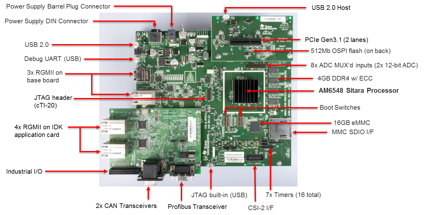
The complete feature set for the AM65x EVM is described in AM65x EVM User Manual. This section only provides description of components that are required to complete basic EVM setup for debugging code using an emulator and Code Composer Studio.
6.3.1.1.1. Supported JTAG Debug Probes (Emulators)
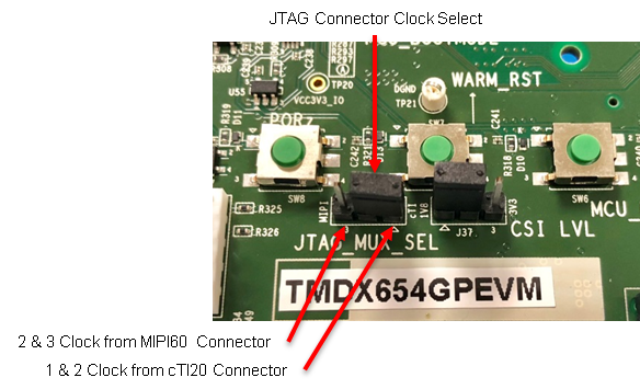
The AM65x EVM includes a cTI20 JTAG connector for external emulators and a micro USB connector for the on-board XDS110 emulator.
For XDS110 connect a USB cable to the micro USB connector J23 on the front of the board.
For external XDS200, connect the emulator to the cTI20 pin connector.
For Lauterbach or emulators with MIPI60 or TI14 pin connector, an adapter must be used to connect the emulator.
Warning
Do not connect an XDS560 emulator to the J16 application board connector. This may damage the EVM and the emulator pod.

If you are using an external emulator pod, you must select which connector sources the clock. The AM65x EVM can support the MIPI60 or cTI20 connector. The JTAG select jumper must be set correctly to specify the clock source as either the MIPI60 or the cTI20 connector.
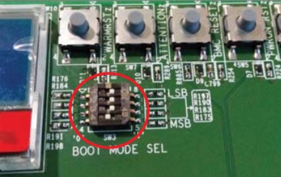
6.3.1.1.2. BOOTMODE Switches
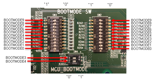
MCU BOOTMODE shown:
MCUBOOTMODE[8:0] – 0000 10 011
Values in bold are fixed with resistors.
BOOTMODE shown:
BOOTMODE[18:0] - 1111111000011110000
6.3.1.1.2.1. Recommended Boot Mode
BOOTMODE[18:0] = 000000000 0000000000 MCUBOOTMODE[8:0]= 000000011 (SLEEP BOOT)
- Boot Settings
- SW2 – All switches OFF
- SW3 – All switches OFF
BOOTMODE[18:0] = 000000100 0000000110 MCUBOOTMODE[8:0]= 000000011 (SD BOOT)
For full details on supported boot modes, please refer to the table below.
| SW3.4 | SW3.3 | SW3.2 | SW3.1 | Primary Boot Device Selected |
|---|---|---|---|---|
| OFF | OFF | OFF | OFF | Sleep (No boot - debug mode) |
| OFF | OFF | OFF | ON | OSPI |
| OFF | OFF | ON | OFF | QSPI |
| OFF | OFF | ON | ON | Hyperflash |
| OFF | ON | OFF | OFF | SPI (on QSPI/OSPI port 0 in legacy SPI mode) |
| OFF | ON | OFF | ON | I2C |
| OFF | ON | ON | OFF | MMC/SD card, eMMC boot from UDA or file system |
| OFF | ON | ON | ON | Ethernet |
| ON | OFF | OFF | OFF | USB |
| ON | OFF | OFF | ON | PCIe |
| ON | OFF | ON | OFF | UART |
| ON | OFF | ON | ON | Reserved |
| ON | ON | OFF | OFF | GPMC XIP |
| ON | ON | OFF | ON | eMMC boot from boot partition (with auto-fall back to file system) |
| ON | ON | ON | OFF | Reserved (acts as no boot) |
| ON | ON | ON | ON | Reserved (acts as no boot) |
Note
On the AM65x EVM, ensure that the PLL configuration is set to 25 MHz (see bolded line in table below).
| Bit 2 | Bit 1 | Bit 0 | PLL REF CLK (MHz) |
|---|---|---|---|
| 0 | 0 | 0 | Sleep (No boot - debug mode) |
| 0 | 0 | 1 | 20 |
| 0 | 1 | 0 | 24 |
| 0 | 1 | 1 | 25 |
| 1 | 0 | 0 | 26 |
| 1 | 0 | 1 | 27 |
| 1 | 1 | 0 | Reserved |
| 1 | 1 | 1 | No PLL Configuration Done (slow speed backup) |
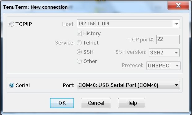
6.3.1.1.3. UART Connection
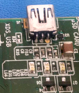
- Connect a micro USB cable between UART port (J42) of the EVM and host PC.
- Open a serial console (e.g. Tera Term) on host PC, connect to COM port on which SOC UART0 port is connected. Four COM ports should appear in the serial console application. Connect to the first COM port in the list.
- First COM port – SoC MAIN UART0
- Second COM port – MCU UART
- Third COM port – Wakeup UART
- Fourth COM port – SoC MAIN UART1
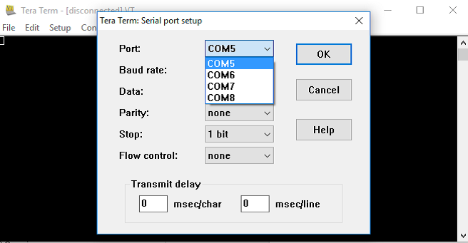
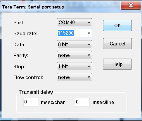
- Open a serial console (e.g Tera Term) on host PC, connect to COM port on which EVM UART port is connected and set the following configuration.
- Baud rate - 115200
- Data length - 8 bit
- Parity - None
- Stop bits - 1
- Flow control - None
6.3.1.1.4. Powering the EVM
| Connector | Specifications | Example |
|---|---|---|
| Power DIN, 4-pin | 24VDC, 5A Output (Max) | CUI Inc.SDI120-24-U-P51 |
| Barrel Plug, 2.5mm I.D x 5.5mm O.D x 9.55 | 12-24VDC, positive center, 2.71A Output (Max) | CUI Inc. SDI65-24UD-P6 |
Note
The DIN connector power supply is recommended to provide enough power for applications that make use of the PCIe interface.
6.3.1.2. Minimum Hardware Setup Required to Connect to EVM
- Connect micro USB cable to J23 and connect USB to Host PC on which CCS is installed.
- Connect micro USB cable to J42 for UART serial IO.
- Set boot switches to “Sleep Boot” or “SD Boot” as described in the BOOT Switches section.
- Connect power supply to DC jack and power on EVM.
- Set switches and jumpers as indicated below.
- Boot Settings
- SW2 - All switches OFF
- SW3 - All switches OFF
- Jumpers
- J4 – Short all the pins
- JP37 – Short pins 1 & 2
- J43 - Short pins 1 & 2
- J8 – Short pins 1 & 2
6.3.1.3. AM65x Debug Software Setup
The following software packages are required to setup the AM65x EVM
- Code Composer Studio IDE Environment
- Processor SDK RTOS for AM65xx
6.3.1.3.1. CCS Host Setup
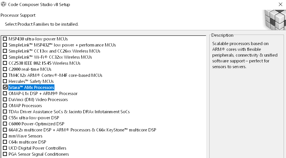
1. Download CCS from the following link: https://processors.wiki.ti.com/index.php/Download_CCS
Note
Check the Processor SDK Release Notes for the recommended CCS version.
Ensure that at least “Sitara AMx Processors” is selected:
6.3.1.3.1.1. Install the latest Emulation Package and Device Support Package
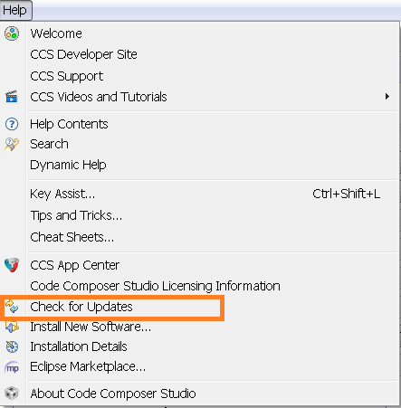
1. In CCS, navigate to Help -> Check for Updates and select “Sitara device support” and “TI Emulators” and click Next.
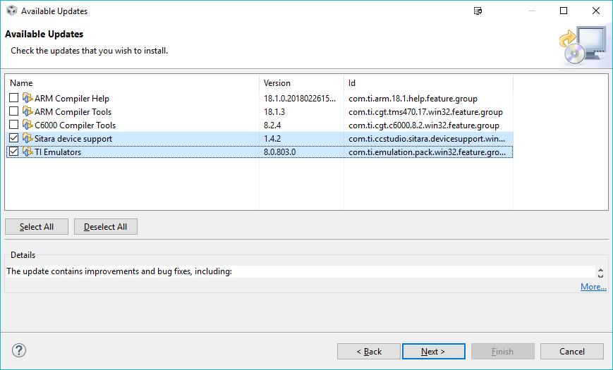
2. Click “Next” again, select “I accept the terms of the license agreements” and click Finish to begin the installation.
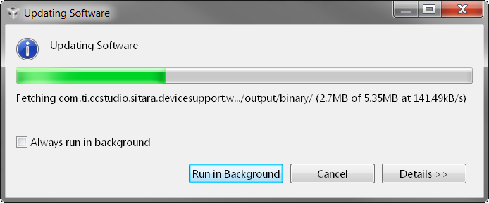
3. You may be prompted to restart CCS for the updates to take effect. Click “Restart Now” when prompted to complete the installation.
Disable Automatic Updates
To disable automatic updates in CCS, navigate to Windows -> Preferences -> Install/Update -> Automatic Updates, and uncheck “Automatically find new updates and notify me.”
This is a precautionary step to avoid automatic updates overwriting files updated through TI Emulation Updates for AM65x
6.3.1.3.2. Basic CCS Setup
The Basic CCS setup is similar to earlier Sitara devices which involves creation of target configuration and connecting to cores using the GEL files. This step is suitable for new board bring up and getting hello world going on the AM65x cores.
Users can use this setup for benchmarking code on cores, test basic pin functionality or to run diagnostics. However, multi-core application developers requiring resource management, power management or security services will require the advanced CCS setup in addition to the basic core setup.
We recommend that you follow the steps in basic setup and then migrate to the advanced SOC CCS setup for application development.
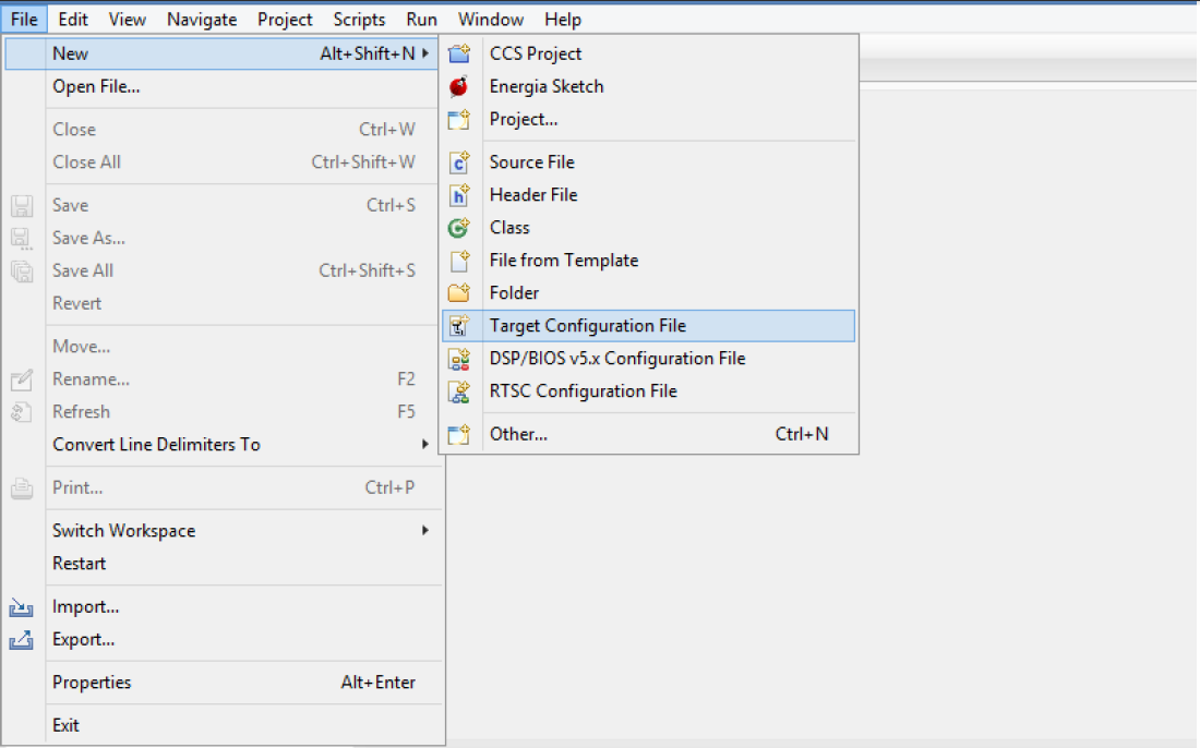
6.3.1.3.2.1. Creating the Target Configuration
- In CCS, open the Target Configurations window by navigating to View -> Target Configurations.
- In Target Configurations, right click and select “New Target Configuration.”
- Populate the Target Configuration File name, set the location, and click Finish.
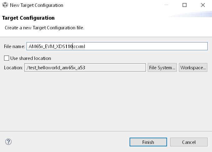
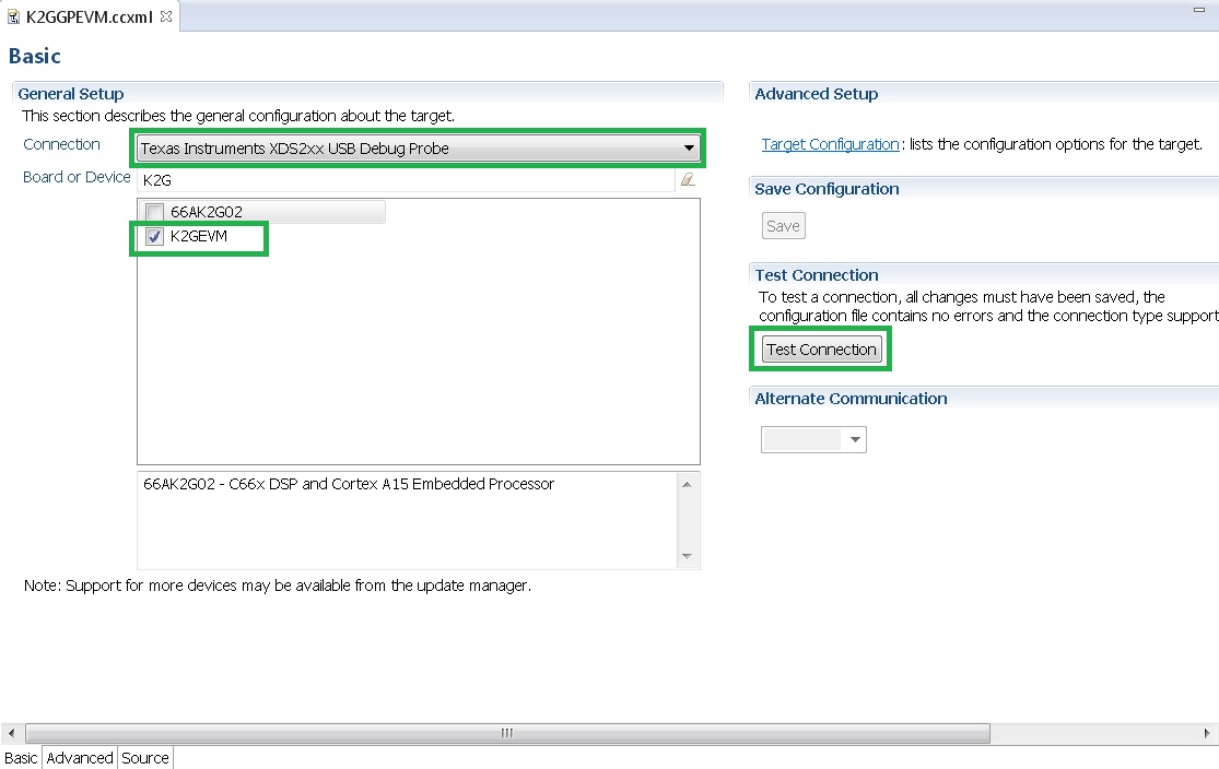
- Select “Texas Instruments XDS110 USB Debug Probe” for the Connection and “GPEVM_AM65x” for the Board or Device.
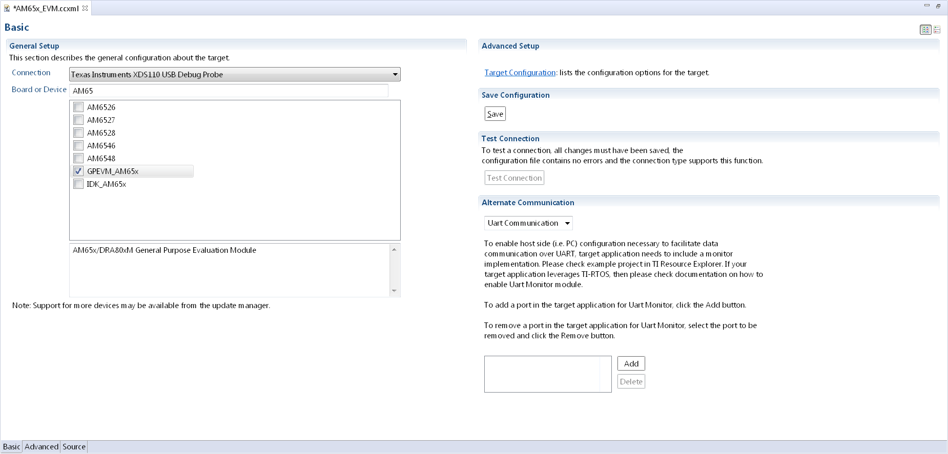
Note
The GEL files are automatically populated in the Target Configuration when selecting an EVM instead of an SOC. The SOC option is generally used for custom board bring up or secondary boot debugging.
- Navigate to the “Advanced” tab to ensure the GEL files are populated in the “initialization script” field for the various cores.
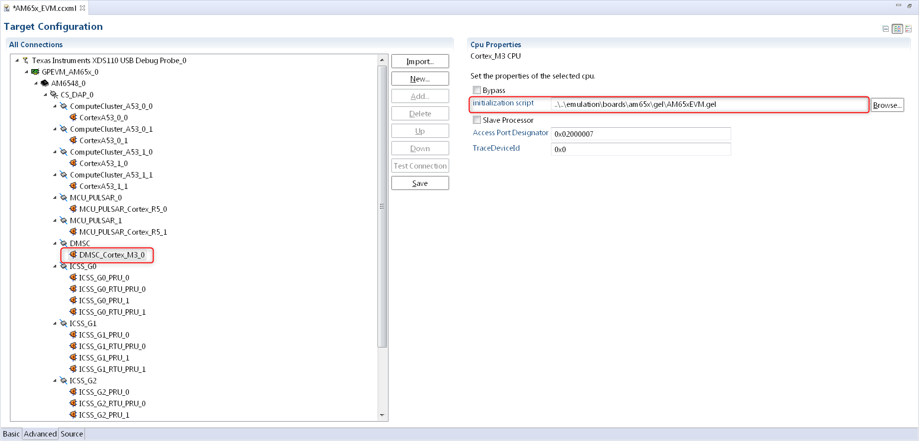
The initialization script for the Cortex M3 will setup the MCU domain and Main domain PLL clocks, PSC registers, and bring the R5 and Cortex A53 cores out of reset.
The initialization script for the Cortex A53 and Cortex R5 will perform a similar step to setup the DDR clocks and initialize DDR from the cores if required.
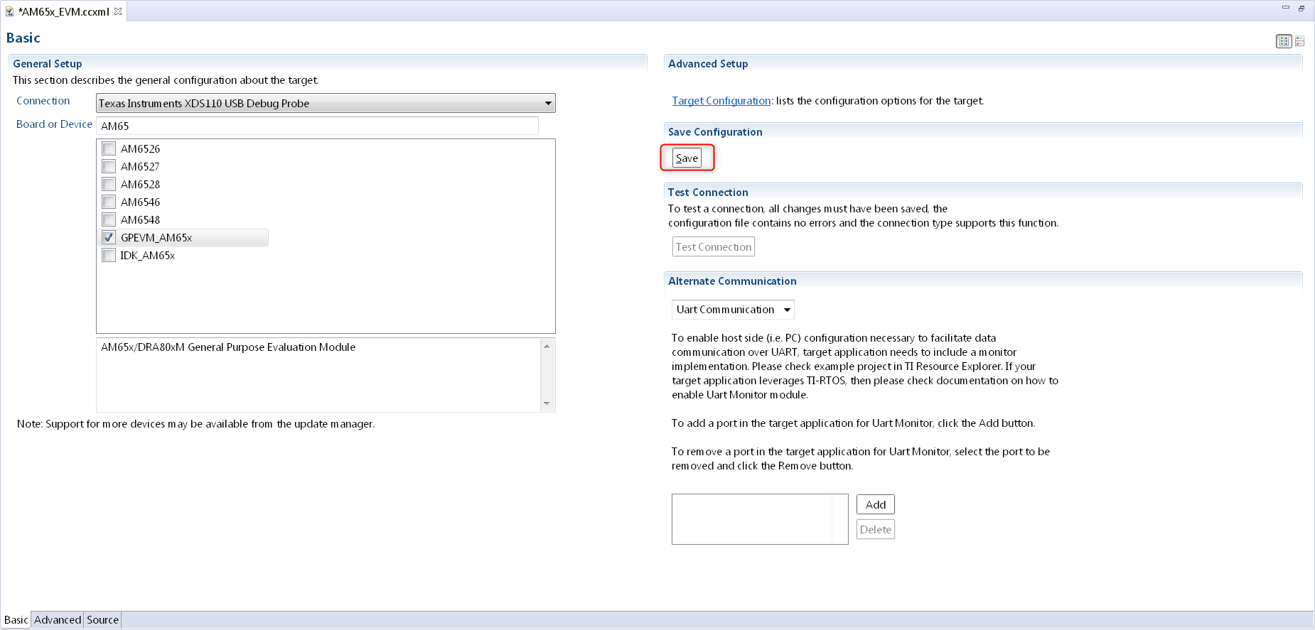
- Save the Target Configuration.
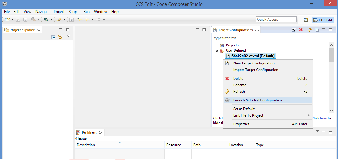
6.3.1.3.2.2. Connecting to the Cores on AM65x
1. Launch Target Configuration In CCS Editor View, go to View -> Target Configuration, and right click on the configuration that was created in the previous section and select “Launch Selected Configuration.”
- Connect to DMSC_Cortex_M3
Note
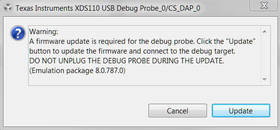
When connecting to the M3 core for the first time, you may be prompted with a firmware update. Please click “Update” to update the emulator firmware.
On AM65x DMSC_Cortex_M3 is the boot master and is the first core that wakes up and starts the R5F ROM. Upon launching the target configuration, connect to DMSC_Cortex_M3 first, as this will automatically perform the PSC and PLL initialization. The following GEL output will appear in the CCS Console:
DMSC_Cortex_M3_0: GEL Output: Configuring AM65xEVM...
DMSC_Cortex_M3_0: GEL Output: Init value actual value: 0x00000888
DMSC_Cortex_M3_0: GEL Output: Register value: 0x00000888
DMSC_Cortex_M3_0: GEL Output: ATCM is on
DMSC_Cortex_M3_0: GEL Output: ATCM configured.
DMSC_Cortex_M3_0: GEL Output: Assuming execution from M3
DMSC_Cortex_M3_0: GEL Output: This script sets the first address translation region to [0x8000_0000, 0x0000_0000].
DMSC_Cortex_M3_0: GEL Output: It also sets the second address translation region to    [0x6000_0000, 0x4000_0000].
DMSC_Cortex_M3_0: GEL Output: Setting all PLLs in progress. This may take some time.
DMSC_Cortex_M3_0: GEL Output: 0 Percent Complete...
DMSC_Cortex_M3_0: GEL Output: 10 Percent Complete...
DMSC_Cortex_M3_0: GEL Output: 20 Percent Complete...
DMSC_Cortex_M3_0: GEL Output: 30 Percent Complete...
DMSC_Cortex_M3_0: GEL Output: 40 Percent Complete...
DMSC_Cortex_M3_0: GEL Output: 50 Percent Complete...
DMSC_Cortex_M3_0: GEL Output: 60 Percent Complete...
DMSC_Cortex_M3_0: GEL Output: 70 Percent Complete...
DMSC_Cortex_M3_0: GEL Output: 80 Percent Complete...
DMSC_Cortex_M3_0: GEL Output: 90 Percent Complete...
DMSC_Cortex_M3_0: GEL Output: Setting all PLLs done!
DMSC_Cortex_M3_0: GEL Output: Powering up all PSC power domains in progress...
DMSC_Cortex_M3_0: GEL Output: Powering up LPSC_WKUP_COMMON
DMSC_Cortex_M3_0: GEL Output: No change needed.
DMSC_Cortex_M3_0: GEL Output: Powering up LPSC_DMSC
DMSC_Cortex_M3_0: GEL Output: No change needed.
DMSC_Cortex_M3_0: GEL Output: Powering up LPSC_WKUP2MCU
DMSC_Cortex_M3_0: GEL Output: No change needed.
DMSC_Cortex_M3_0: GEL Output: Powering up LPSC_WKUP2MAIN_INFRA
DMSC_Cortex_M3_0: GEL Output: No change needed.
DMSC_Cortex_M3_0: GEL Output: Powering up LPSC_DEBUG2DMSC
DMSC_Cortex_M3_0: GEL Output: No change needed.
DMSC_Cortex_M3_0: GEL Output: Powering up LPSC_WKUP_GPIO
DMSC_Cortex_M3_0: GEL Output: No change needed.
DMSC_Cortex_M3_0: GEL Output: Powering up LPSC_MCU2MAIN_INFRA
DMSC_Cortex_M3_0: GEL Output: No change needed.
DMSC_Cortex_M3_0: GEL Output: Powering up LPSC_MCU2MAIN
DMSC_Cortex_M3_0: GEL Output: No change needed.
DMSC_Cortex_M3_0: GEL Output: Powering up LPSC_MCU2WKUP
DMSC_Cortex_M3_0: GEL Output: No change needed.
DMSC_Cortex_M3_0: GEL Output: Powering up LPSC_MAIN2MCU
DMSC_Cortex_M3_0: GEL Output: No change needed.
DMSC_Cortex_M3_0: GEL Output: Powering up LPSC_MCU_COMMON
DMSC_Cortex_M3_0: GEL Output: No change needed.
DMSC_Cortex_M3_0: GEL Output: Powering up LPSC_MCU_TEST
DMSC_Cortex_M3_0: GEL Output: No change needed.
DMSC_Cortex_M3_0: GEL Output: Powering up LPSC_MCU_MCAN_0
DMSC_Cortex_M3_0: GEL Output: No change needed.
DMSC_Cortex_M3_0: GEL Output: Powering up LPSC_MCU_MCAN_1
DMSC_Cortex_M3_0: GEL Output: No change needed.
DMSC_Cortex_M3_0: GEL Output: Powering up LPSC_MCU_OSPI_0
DMSC_Cortex_M3_0: GEL Output: No change needed.
DMSC_Cortex_M3_0: GEL Output: Powering up LPSC_MCU_OSPI_1
DMSC_Cortex_M3_0: GEL Output: No change needed.
DMSC_Cortex_M3_0: GEL Output: Powering up LPSC_MCU_HYPERBUS
DMSC_Cortex_M3_0: GEL Output: No change needed.
DMSC_Cortex_M3_0: GEL Output: Powering up LPSC_MCU_DEBUG
DMSC_Cortex_M3_0: GEL Output: No change needed.
DMSC_Cortex_M3_0: GEL Output: Powering up LPSC_MCU_R5_0
DMSC_Cortex_M3_0: GEL Output: No change needed.
DMSC_Cortex_M3_0: GEL Output: Powering up LPSC_MCU_R5_1
DMSC_Cortex_M3_0: GEL Output: No change needed.
DMSC_Cortex_M3_0: GEL Output: Powering up LPSC_MAIN_INFRA
DMSC_Cortex_M3_0: GEL Output: No change needed.
DMSC_Cortex_M3_0: GEL Output: Powering up LPSC_MAIN_TEST
DMSC_Cortex_M3_0: GEL Output: No change needed.
DMSC_Cortex_M3_0: GEL Output: Powering up LPSC_MAIN_PBIST
DMSC_Cortex_M3_0: GEL Output: No change needed.
DMSC_Cortex_M3_0: GEL Output: Powering up LPSC_CC_TOP
DMSC_Cortex_M3_0: GEL Output: No change needed.
DMSC_Cortex_M3_0: GEL Output: Powering up LPSC_A53_CLUSTER_0
DMSC_Cortex_M3_0: GEL Output: Power domain and module state changed successfully.
DMSC_Cortex_M3_0: GEL Output: Powering up LPSC_A53_0
DMSC_Cortex_M3_0: GEL Output: Power domain and module  state changed successfully.
DMSC_Cortex_M3_0: GEL Output: Powering up LPSC_A53_1
DMSC_Cortex_M3_0: GEL Output: Power domain and module state changed successfully.
DMSC_Cortex_M3_0: GEL Output: Powering up LPSC_A53_CLUSTER_1
DMSC_Cortex_M3_0: GEL Output: Power domain and module state changed successfully.
DMSC_Cortex_M3_0: GEL Output: Powering up LPSC_A53_2
DMSC_Cortex_M3_0: GEL Output: Power domain and module state changed successfully.
DMSC_Cortex_M3_0: GEL Output: Powering up LPSC_A53_3
DMSC_Cortex_M3_0: GEL Output: Power domain and module state changed successfully.
DMSC_Cortex_M3_0: GEL Output: Powering up LPSC_MAIN_DEBUG
DMSC_Cortex_M3_0: GEL Output: No change needed.
DMSC_Cortex_M3_0: GEL Output: Powering up LPSC_DSS
DMSC_Cortex_M3_0: GEL Output: Power domain and module state changed successfully.
DMSC_Cortex_M3_0: GEL Output: Powering up LPSC_MMC
DMSC_Cortex_M3_0: GEL Output: No change needed.
DMSC_Cortex_M3_0: GEL Output: Powering up LPSC_CAL
DMSC_Cortex_M3_0: GEL Output: Power domain and module state changed successfully.
DMSC_Cortex_M3_0: GEL Output: Powering up LPSC_PCIE_0
DMSC_Cortex_M3_0: GEL Output: Power domain and module state changed successfully.
DMSC_Cortex_M3_0: GEL Output: Powering up LPSC_PCIE_1
DMSC_Cortex_M3_0: GEL Output: Power domain and module state changed successfully.
DMSC_Cortex_M3_0: GEL Output: Powering up LPSC_USB_0
DMSC_Cortex_M3_0: GEL Output: Power domain and module state changed successfully.
DMSC_Cortex_M3_0: GEL Output: Powering up LPSC_USB_1
DMSC_Cortex_M3_0: GEL Output: Power domain and module state changed successfully.
DMSC_Cortex_M3_0: GEL Output: Powering up LPSC_SAUL
DMSC_Cortex_M3_0: GEL Output: No change needed.
DMSC_Cortex_M3_0: GEL Output: Powering up LPSC_PER_COMMON
DMSC_Cortex_M3_0: GEL Output: No change needed.
DMSC_Cortex_M3_0: GEL Output: Powering up LPSC_NB
DMSC_Cortex_M3_0: GEL Output: No change needed.
DMSC_Cortex_M3_0: GEL Output: Powering up LPSC_SERDES_0
DMSC_Cortex_M3_0: GEL Output: Power domain and module state changed successfully.
DMSC_Cortex_M3_0: GEL Output: Powering up LPSC_SERDES_1
DMSC_Cortex_M3_0: GEL Output: Power domain and module state changed successfully.
DMSC_Cortex_M3_0: GEL Output: Powering up LPSC_ICSSG_0
DMSC_Cortex_M3_0: GEL Output: Power domain and module state changed successfully.
DMSC_Cortex_M3_0: GEL Output: Powering up LPSC_ICSSG_1
DMSC_Cortex_M3_0: GEL Output: Power domain and module state changed successfully.
DMSC_Cortex_M3_0: GEL Output: Powering up LPSC_ICSSG_2
DMSC_Cortex_M3_0: GEL Output: Power domain and module state changed successfully.
DMSC_Cortex_M3_0: GEL Output: Powering up LPSC_GPU
DMSC_Cortex_M3_0: GEL Output: Power domain and module state changed successfully.
DMSC_Cortex_M3_0: GEL Output: Powering up LPSC_EMIF_DATA
DMSC_Cortex_M3_0: GEL Output: Power domain and module state changed successfully.
DMSC_Cortex_M3_0: GEL Output: Powering up LPSC_EMIF_CFG
DMSC_Cortex_M3_0: GEL Output: Power domain and module state changed successfully.
DMSC_Cortex_M3_0: GEL Output: Powering up all PSC power domains done!
3. Connect to Cortex A53 or Cortex R5F Users must now connect to either the Cortex A53 (CortexA53_0_0) or Cortex R5 (MCU_PULSAR_Cortex_R5_0). The following GEL output will appear in the CCS console when connecting to the Cortex A53:
CortexA53_0_0: GEL Output: VTT Regulator Enabled
CortexA53_0_0: GEL Output:
PHY Init complete
CortexA53_0_0: GEL Output: DDRSS_DDRPHY_PGSR0 = 0x8000000F
CortexA53_0_0: GEL Output:
Waiting for DRAM Init to complete...
CortexA53_0_0: GEL Output:
DRAM Init complete
CortexA53_0_0: GEL Output: DDRSS_DDRPHY_PGSR0 = 0x8000001F
CortexA53_0_0: GEL Output:
Waiting for write leveling to complete
CortexA53_0_0: GEL Output:
Write leveling complete
CortexA53_0_0: GEL Output: DDRSS_DDRPHY_PGSR0 = 0x8000003F
CortexA53_0_0: GEL Output: checking status per byte...
CortexA53_0_0: GEL Output:
DDRSS_DDRPHY_DX0GSR0 = 0x00932420
CortexA53_0_0: GEL Output:
DDRSS_DDRPHY_DX1GSR0 = 0x009224A0
CortexA53_0_0: GEL Output:
DDRSS_DDRPHY_DX2GSR0 = 0x00992620
CortexA53_0_0: GEL Output:
DDRSS_DDRPHY_DX3GSR0 = 0x009825A0
CortexA53_0_0: GEL Output:
Waiting for Read DQS training to complete
CortexA53_0_0: GEL Output:
Read DQS training complete
CortexA53_0_0: GEL Output: DDRSS_DDRPHY_PGSR0 = 0x8000007F
CortexA53_0_0: GEL Output: checking status per byte...
CortexA53_0_0: GEL Output:
DDRSS_DDRPHY_DX0RSR0 = 0x00000000
CortexA53_0_0: GEL Output:
DDRSS_DDRPHY_DX1RSR0 = 0x00000000
CortexA53_0_0: GEL Output:
DDRSS_DDRPHY_DX2RSR0 = 0x00000000
CortexA53_0_0: GEL Output:
DDRSS_DDRPHY_DX3RSR0 = 0x00000000
CortexA53_0_0: GEL Output:
Waiting for Write leveling adjustment to complete
CortexA53_0_0: GEL Output:
Write leveling adjustment complete
CortexA53_0_0: GEL Output: DDRSS_DDRPHY_PGSR0 = 0x800000FF
CortexA53_0_0: GEL Output:
Waiting for Read deskew to complete
CortexA53_0_0: GEL Output:
Read deskew complete
CortexA53_0_0: GEL Output: DDRSS_DDRPHY_PGSR0 = 0x800001FF
CortexA53_0_0: GEL Output:
Waiting for Write deskew to complete
CortexA53_0_0: GEL Output:
Write deskew complete
CortexA53_0_0: GEL Output: DDRSS_DDRPHY_PGSR0 = 0x800003FF
CortexA53_0_0: GEL Output:
Waiting for Read Eye training to complete
CortexA53_0_0: GEL Output:
Read Eye training complete
CortexA53_0_0: GEL Output: DDRSS_DDRPHY_PGSR0 = 0x800007FF
CortexA53_0_0: GEL Output:
Waiting for Write Eye training to complete
CortexA53_0_0: GEL Output:
Write Eye training complete
CortexA53_0_0: GEL Output: DDRSS_DDRPHY_PGSR0 = 0x80000FFF
CortexA53_0_0: GEL Output:
Waiting for VREF training to complete
CortexA53_0_0: GEL Output:
VREF training complete
CortexA53_0_0: GEL Output: DDRSS_DDRPHY_PGSR0 = 0x80004FFF
CortexA53_0_0: GEL Output:

====

DDR4 Initialization has PASSED!!!!

====
The same GEL output will be shown if connecting to the Cortex R5 first instead of the Cortex A53.
- The EVM is now completely initialized to load and run code on the cores and access the full device address range. User level software is responsible to configure the pin multiplexing and peripheral configuration.
6.3.1.3.3. Advanced AM65x Debug Setup with DMSC Firmware Load
Description
AM65x EVM users testing basic functionality like R5F and A53 bring up and DDR configuration can use the basic setup described in the previous section for setting up the EVM. However, advanced application level debug that uses resource management for UDMAs, interrupt setup, power management to setup clock modules, or wakeup/power of slave cores will require loading of SYSFW (DMSC Firmware) on the M3 core so that the application can make API calls to leverage its services.
To load the SYSFW firmware, the DMSC ROM expects R5F secondary bootloader/application to provide board configuration message to initialize the cores and SOC services. The R5F application provided in SciClient uses a default board configuration message to the SYSFW and sets up the device for application debugging.
For more details, refer to the Initialization Chapter in the TRM and the SciClient User guide.
Additional Software Dependency
- Processor SDK RTOS for AM65x
Users are required to install Processor SDK RTOS to obtain the SciClient component package before proceeding to the Next Step.
After installing Processor SDK RTOS, users should locate the latest R5F CCS init app, SYSFW binary, and the debug server script within the following directory:
${PDK_INSTALL_PATH}/packages/ti/drv/sciclient/tools/ccsLoadDmsc
The following files are provided as part for the SciClient tools:
- launch_am65xx.js: CCS Debug Server script to perform on target connect and load DMSC firmware and R5F CCS Init app.
Location:: ${PDK_INSTALL_PATH}/packages/ti/drv/sciclient/tools/ccsLoadDmsc
- sciclient_ccs_init_mcu1_0_release.xer5f: R5F Application with default board config
Location:: ${PDK_INSTALL_PATH}/packages/ti/drv/sciclient/tools/ccsLoadDmsc/am65xx
- ti-sci-firmware-am6x-gp.bin: TISCI SYSFW binary loaded on the DMSC
Location:: ${PDK_INSTALL_PATH}/packages/ti/drv/sciclient/src/V0
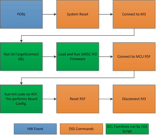
AM65x Advanced Debug Script Flow
6.3.1.3.3.1. Creating Debug Configuration to Integrate CCS GEL and DMSC Firmware Initialization
With the intent to maintain the same CCS target connect flow as existing devices, we provide a Debug Server Script (DSS) that users can link to in their target configuration to allow for loading SYSFW firmware on the DMSC as part of the target connect process.
The DSS script allows users to perform all of the initialization using a single click. When the script is run, the following actions happens sequentially:
- Running On Target Connect M3 existing GEL scripts.
- Loading the DMSC firmware
*.bin file to DMSC M3. - Run the R5F Init code which performs the board configuration initialization.
At the end of the setup, the R5F and A53 are in a clean state to load code and debug the application with the SYSFW loaded on the M3 core.
Steps to Link and Run the DSS Script for DMSC Firmware Loading
- Update the file “pdk/packages/ti/drv/sciclient/tools/ccsLoadDmsc/launch_am65xx.js” for the following variable to your PC location:
     //<!!!!!! EDIT THIS !!!!!>
     // Set this to 1 to allow loading the GEL files directly from the ccxml file.
     disableGelLoad = 1;
     if (disableGelLoad == 0)
     {
     //Path to GEL files
     gelFilePath = "C:/ti/ccsv8/ccs_base/emulation/gel/AM65xEVM";
     }
     // Path to the directory in which this file would be residing. CCS expects
     // absolute paths to load the binaries.
     thisJsFileDirectory = "pdk/packages/ti/drv/sciclient/tools/ccsLoadDmsc";
     //<!!!!!! EDIT THIS !!!!!>
- Set disableGelLoad =1 if GEL files is linked to the cores in the target configuration file.
- The variable “gelFilePath” doesn’t need to be updated if CCS is installed in the default C:/ti/ directory.
- The variable “thisJsFileDirectory” needs to be updated to point to the PDK install directory.
- Connect the Javascript to the CCXML file with the steps shown below.
Note
This step needs to be repeated if you switch workspaces or clean your workspace.
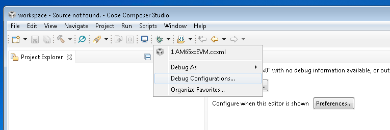
In the debug view after completing the basic CCS setup, Click on Debug Configurations from the button as show below:
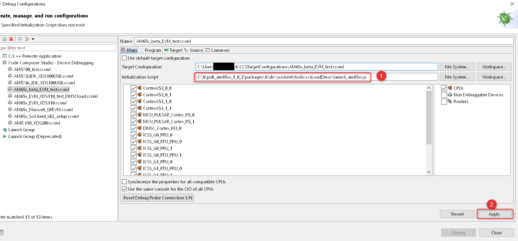
Select the CCXML file from the left-hand side and populate the path to the launch_am65xx.js file in the “Initialization Script” free form field and click on “Apply”.
Once you Launch the CCXML file, the java script will automatically run and connect to R5F.
Steps to re-run the script once ccxml is already launched:
In the CCS window, navigate to “View → Scripting Console.”
In the CCS Scripting Console, type:
> load ("<Your Path>\\launch_am65xx.js");
This would give the following output on the scripting console:
js:> load("C:\\Users\\User\\Documents\\PDK\\pdk\\packages\\ti\\drv\\sciclient\\tools\\ccsLoadDmsc\\launch_am65xx.js")
Connecting to DMSC_Cortex_M3_0!
Loading DMSC Firmware...
DMSC Firmware Load Done...
DMSC Firmware run starting now...
Connecting to MCU Cortex_R5_0!
GEL Output Log:
DMSC_Cortex_M3_0: GEL Output: Configuring AM65xEVM...
DMSC_Cortex_M3_0: GEL Output: Init value actual value: 0x00000888
DMSC_Cortex_M3_0: GEL Output: Register value: 0x00000888
DMSC_Cortex_M3_0: GEL Output: ATCM is on
DMSC_Cortex_M3_0: GEL Output: ATCM configured.
DMSC_Cortex_M3_0: GEL Output: Assuming execution from M3
DMSC_Cortex_M3_0: GEL Output: This script sets the first address translation region to [0x8000_0000, 0x0000_0000].
DMSC_Cortex_M3_0: GEL Output: It also sets the second address translation region to    [0x6000_0000, 0x4000_0000].
DMSC_Cortex_M3_0: GEL Output: Setting all PLLs in progress. This may take some time.
DMSC_Cortex_M3_0: GEL Output: 0 Percent Complete...
DMSC_Cortex_M3_0: GEL Output: 10 Percent Complete...
DMSC_Cortex_M3_0: GEL Output: 20 Percent Complete...
DMSC_Cortex_M3_0: GEL Output: 30 Percent Complete...
DMSC_Cortex_M3_0: GEL Output: 40 Percent Complete...
DMSC_Cortex_M3_0: GEL Output: 50 Percent Complete...
DMSC_Cortex_M3_0: GEL Output: 60 Percent Complete...
DMSC_Cortex_M3_0: GEL Output: 70 Percent Complete...
DMSC_Cortex_M3_0: GEL Output: 80 Percent Complete...
DMSC_Cortex_M3_0: GEL Output: 90 Percent Complete...
DMSC_Cortex_M3_0: GEL Output: Setting all PLLs done!
DMSC_Cortex_M3_0: GEL Output: Powering up all PSC power domains in progress...
DMSC_Cortex_M3_0: GEL Output: Powering up LPSC_WKUP_COMMON
DMSC_Cortex_M3_0: GEL Output: No change needed.
DMSC_Cortex_M3_0: GEL Output: Powering up LPSC_DMSC
DMSC_Cortex_M3_0: GEL Output: No change needed.
DMSC_Cortex_M3_0: GEL Output: Powering up LPSC_WKUP2MCU
DMSC_Cortex_M3_0: GEL Output: No change needed.
DMSC_Cortex_M3_0: GEL Output: Powering up LPSC_WKUP2MAIN_INFRA
DMSC_Cortex_M3_0: GEL Output: No change needed.
DMSC_Cortex_M3_0: GEL Output: Powering up LPSC_DEBUG2DMSC
DMSC_Cortex_M3_0: GEL Output: No change needed.
DMSC_Cortex_M3_0: GEL Output: Powering up LPSC_WKUP_GPIO
DMSC_Cortex_M3_0: GEL Output: No change needed.
DMSC_Cortex_M3_0: GEL Output: Powering up LPSC_MCU2MAIN_INFRA
DMSC_Cortex_M3_0: GEL Output: No change needed.
DMSC_Cortex_M3_0: GEL Output: Powering up LPSC_MCU2MAIN
DMSC_Cortex_M3_0: GEL Output: No change needed.
DMSC_Cortex_M3_0: GEL Output: Powering up LPSC_MCU2WKUP
DMSC_Cortex_M3_0: GEL Output: No change needed.
DMSC_Cortex_M3_0: GEL Output: Powering up LPSC_MAIN2MCU
DMSC_Cortex_M3_0: GEL Output: No change needed.
DMSC_Cortex_M3_0: GEL Output: Powering up LPSC_MCU_COMMON
DMSC_Cortex_M3_0: GEL Output: No change needed.
DMSC_Cortex_M3_0: GEL Output: Powering up LPSC_MCU_TEST
DMSC_Cortex_M3_0: GEL Output: No change needed.
DMSC_Cortex_M3_0: GEL Output: Powering up LPSC_MCU_MCAN_0
DMSC_Cortex_M3_0: GEL Output: No change needed.
DMSC_Cortex_M3_0: GEL Output: Powering up LPSC_MCU_MCAN_1
DMSC_Cortex_M3_0: GEL Output: No change needed.
DMSC_Cortex_M3_0: GEL Output: Powering up LPSC_MCU_OSPI_0
DMSC_Cortex_M3_0: GEL Output: No change needed.
DMSC_Cortex_M3_0: GEL Output: Powering up LPSC_MCU_OSPI_1
DMSC_Cortex_M3_0: GEL Output: No change needed.
DMSC_Cortex_M3_0: GEL Output: Powering up LPSC_MCU_HYPERBUS
DMSC_Cortex_M3_0: GEL Output: No change needed.
DMSC_Cortex_M3_0: GEL Output: Powering up LPSC_MCU_DEBUG
DMSC_Cortex_M3_0: GEL Output: No change needed.
DMSC_Cortex_M3_0: GEL Output: Powering up LPSC_MCU_R5_0
DMSC_Cortex_M3_0: GEL Output: No change needed.
DMSC_Cortex_M3_0: GEL Output: Powering up LPSC_MCU_R5_1
DMSC_Cortex_M3_0: GEL Output: No change needed.
DMSC_Cortex_M3_0: GEL Output: Powering up LPSC_MAIN_INFRA
DMSC_Cortex_M3_0: GEL Output: No change needed.
DMSC_Cortex_M3_0: GEL Output: Powering up LPSC_MAIN_TEST
DMSC_Cortex_M3_0: GEL Output: No change needed.
DMSC_Cortex_M3_0: GEL Output: Powering up LPSC_MAIN_PBIST
DMSC_Cortex_M3_0: GEL Output: No change needed.
DMSC_Cortex_M3_0: GEL Output: Powering up LPSC_CC_TOP
DMSC_Cortex_M3_0: GEL Output: No change needed.
DMSC_Cortex_M3_0: GEL Output: Powering up LPSC_A53_CLUSTER_0
DMSC_Cortex_M3_0: GEL Output: Power domain and module state changed successfully.
DMSC_Cortex_M3_0: GEL Output: Powering up LPSC_A53_0
DMSC_Cortex_M3_0: GEL Output: Power domain and module state changed successfully.
DMSC_Cortex_M3_0: GEL Output: Powering up LPSC_A53_1
DMSC_Cortex_M3_0: GEL Output: Power domain and module state changed successfully.
DMSC_Cortex_M3_0: GEL Output: Powering up LPSC_A53_CLUSTER_1
DMSC_Cortex_M3_0: GEL Output: Power domain and module state changed successfully.
DMSC_Cortex_M3_0: GEL Output: Powering up LPSC_A53_2
DMSC_Cortex_M3_0: GEL Output: Power domain and module state changed successfully.
DMSC_Cortex_M3_0: GEL Output: Powering up LPSC_A53_3
DMSC_Cortex_M3_0: GEL Output: Power domain and module state changed successfully.
DMSC_Cortex_M3_0: GEL Output: Powering up LPSC_MAIN_DEBUG
DMSC_Cortex_M3_0: GEL Output: No change needed.
DMSC_Cortex_M3_0: GEL Output: Powering up LPSC_DSS
DMSC_Cortex_M3_0: GEL Output: Power domain and module state changed successfully.
DMSC_Cortex_M3_0: GEL Output: Powering up LPSC_MMC
DMSC_Cortex_M3_0: GEL Output: Power domain and module state changed successfully.
DMSC_Cortex_M3_0: GEL Output: Powering up LPSC_CAL
DMSC_Cortex_M3_0: GEL Output: Power domain and module state changed successfully.
DMSC_Cortex_M3_0: GEL Output: Powering up LPSC_PCIE_0
DMSC_Cortex_M3_0: GEL Output: Power domain and module state changed successfully.
DMSC_Cortex_M3_0: GEL Output: Powering up LPSC_PCIE_1
DMSC_Cortex_M3_0: GEL Output: Power domain and module state changed successfully.
DMSC_Cortex_M3_0: GEL Output: Powering up LPSC_USB_0
DMSC_Cortex_M3_0: GEL Output: Power domain and module state changed successfully.
DMSC_Cortex_M3_0: GEL Output: Powering up LPSC_USB_1
DMSC_Cortex_M3_0: GEL Output: Power domain and module state changed successfully.
DMSC_Cortex_M3_0: GEL Output: Powering up LPSC_SAUL
DMSC_Cortex_M3_0: GEL Output: No change needed.
DMSC_Cortex_M3_0: GEL Output: Powering up LPSC_PER_COMMON
DMSC_Cortex_M3_0: GEL Output: No change needed.
DMSC_Cortex_M3_0: GEL Output: Powering up LPSC_NB
DMSC_Cortex_M3_0: GEL Output: No change needed.
DMSC_Cortex_M3_0: GEL Output: Powering up LPSC_SERDES_0
DMSC_Cortex_M3_0: GEL Output: Power domain and module state changed successfully.
DMSC_Cortex_M3_0: GEL Output: Powering up LPSC_SERDES_1
DMSC_Cortex_M3_0: GEL Output: Power domain and module state changed successfully.
DMSC_Cortex_M3_0: GEL Output: Powering up LPSC_ICSSG_0
DMSC_Cortex_M3_0: GEL Output: Power domain and module state changed successfully.
DMSC_Cortex_M3_0: GEL Output: Powering up LPSC_ICSSG_1
DMSC_Cortex_M3_0: GEL Output: Power domain and module state changed successfully.
DMSC_Cortex_M3_0: GEL Output: Powering up LPSC_ICSSG_2
DMSC_Cortex_M3_0: GEL Output: Power domain and module state changed successfully.
DMSC_Cortex_M3_0: GEL Output: Powering up LPSC_GPU
DMSC_Cortex_M3_0: GEL Output: Power domain and module state changed successfully.
DMSC_Cortex_M3_0: GEL Output: Powering up LPSC_EMIF_DATA
DMSC_Cortex_M3_0: GEL Output: Power domain and module state changed successfully.
DMSC_Cortex_M3_0: GEL Output: Powering up LPSC_EMIF_CFG
DMSC_Cortex_M3_0: GEL Output: Power domain and module state changed successfully.
DMSC_Cortex_M3_0: GEL Output: Powering up all PSC power domains done!
MCU_PULSAR_Cortex_R5_0: GEL Output: VTT Regulator Enabled
MCU_PULSAR_Cortex_R5_0: GEL Output:
PHY Init complete
MCU_PULSAR_Cortex_R5_0: GEL Output: DDRSS_DDRPHY_PGSR0 = 0x8000000F
MCU_PULSAR_Cortex_R5_0: GEL Output:
Waiting for DRAM Init to complete...
MCU_PULSAR_Cortex_R5_0: GEL Output:
DRAM Init complete
MCU_PULSAR_Cortex_R5_0: GEL Output: DDRSS_DDRPHY_PGSR0 = 0x8000001F
MCU_PULSAR_Cortex_R5_0: GEL Output:
Waiting for write leveling to complete
MCU_PULSAR_Cortex_R5_0: GEL Output:
Write leveling complete
MCU_PULSAR_Cortex_R5_0: GEL Output: DDRSS_DDRPHY_PGSR0 = 0x8000003F
MCU_PULSAR_Cortex_R5_0: GEL Output: checking status per byte...
MCU_PULSAR_Cortex_R5_0: GEL Output:
DDRSS_DDRPHY_DX0GSR0 = 0x00A728A0
MCU_PULSAR_Cortex_R5_0: GEL Output:
DDRSS_DDRPHY_DX1GSR0 = 0x00AA2920
MCU_PULSAR_Cortex_R5_0: GEL Output:
DDRSS_DDRPHY_DX2GSR0 = 0x00AB2920
MCU_PULSAR_Cortex_R5_0: GEL Output:
DDRSS_DDRPHY_DX3GSR0 = 0x00AA2A20
MCU_PULSAR_Cortex_R5_0: GEL Output:
Waiting for Read DQS training to complete
MCU_PULSAR_Cortex_R5_0: GEL Output:
Read DQS training complete
MCU_PULSAR_Cortex_R5_0: GEL Output: DDRSS_DDRPHY_PGSR0 = 0x8000007F
MCU_PULSAR_Cortex_R5_0: GEL Output: checking status per byte...
MCU_PULSAR_Cortex_R5_0: GEL Output:
DDRSS_DDRPHY_DX0RSR0 = 0x00000000
MCU_PULSAR_Cortex_R5_0: GEL Output:
DDRSS_DDRPHY_DX1RSR0 = 0x00000000
MCU_PULSAR_Cortex_R5_0: GEL Output:
DDRSS_DDRPHY_DX2RSR0 = 0x00000000
MCU_PULSAR_Cortex_R5_0: GEL Output:
DDRSS_DDRPHY_DX3RSR0 = 0x00000000
MCU_PULSAR_Cortex_R5_0: GEL Output:
Waiting for Write leveling adjustment to complete
MCU_PULSAR_Cortex_R5_0: GEL Output:
Write leveling adjustment complete
MCU_PULSAR_Cortex_R5_0: GEL Output: DDRSS_DDRPHY_PGSR0 = 0x800000FF
MCU_PULSAR_Cortex_R5_0: GEL Output:
Waiting for Read deskew to complete
MCU_PULSAR_Cortex_R5_0: GEL Output:
Read deskew complete
MCU_PULSAR_Cortex_R5_0: GEL Output: DDRSS_DDRPHY_PGSR0 = 0x800001FF
MCU_PULSAR_Cortex_R5_0: GEL Output:
Waiting for Write deskew to complete
MCU_PULSAR_Cortex_R5_0: GEL Output:
Write deskew complete
MCU_PULSAR_Cortex_R5_0: GEL Output: DDRSS_DDRPHY_PGSR0 = 0x800003FF
MCU_PULSAR_Cortex_R5_0: GEL Output:
Waiting for Read Eye training to complete
MCU_PULSAR_Cortex_R5_0: GEL Output:
Read Eye training complete
MCU_PULSAR_Cortex_R5_0: GEL Output: DDRSS_DDRPHY_PGSR0 = 0x800007FF
MCU_PULSAR_Cortex_R5_0: GEL Output:
Waiting for Write Eye training to complete
MCU_PULSAR_Cortex_R5_0: GEL Output:
Write Eye training complete
MCU_PULSAR_Cortex_R5_0: GEL Output: DDRSS_DDRPHY_PGSR0 = 0x80000FFF
MCU_PULSAR_Cortex_R5_0: GEL Output:
Waiting for VREF training to complete
MCU_PULSAR_Cortex_R5_0: GEL Output:
VREF training complete
MCU_PULSAR_Cortex_R5_0: GEL Output: DDRSS_DDRPHY_PGSR0 = 0x80004FFF
MCU_PULSAR_Cortex_R5_0: GEL Output:

====

DDR4 Initialization has PASSED!!!!

====
6.3.1.3.3.2. Additional Notes for GEL Users
R5F in Split Mode Configuration
AM65x EVM ships with the dual Cortex R5F configured in lockstep mode. The AM65x EVM GEL file provides a GEL function “Change_MCUSS_to_SplitMode” that can be added to OnTargetConnect or invoked from the DMSC_Cortex_M3 to set the dual R5F in split mode.
Configuring PRU-ICSS in Sync Mode
The PRU-ICSS subsystem can be configured to SYNC mode (250 Mhz) using the GEL function “PRU_ICSSG_SyncMode_250MHz” from Cortex A53 or R5F
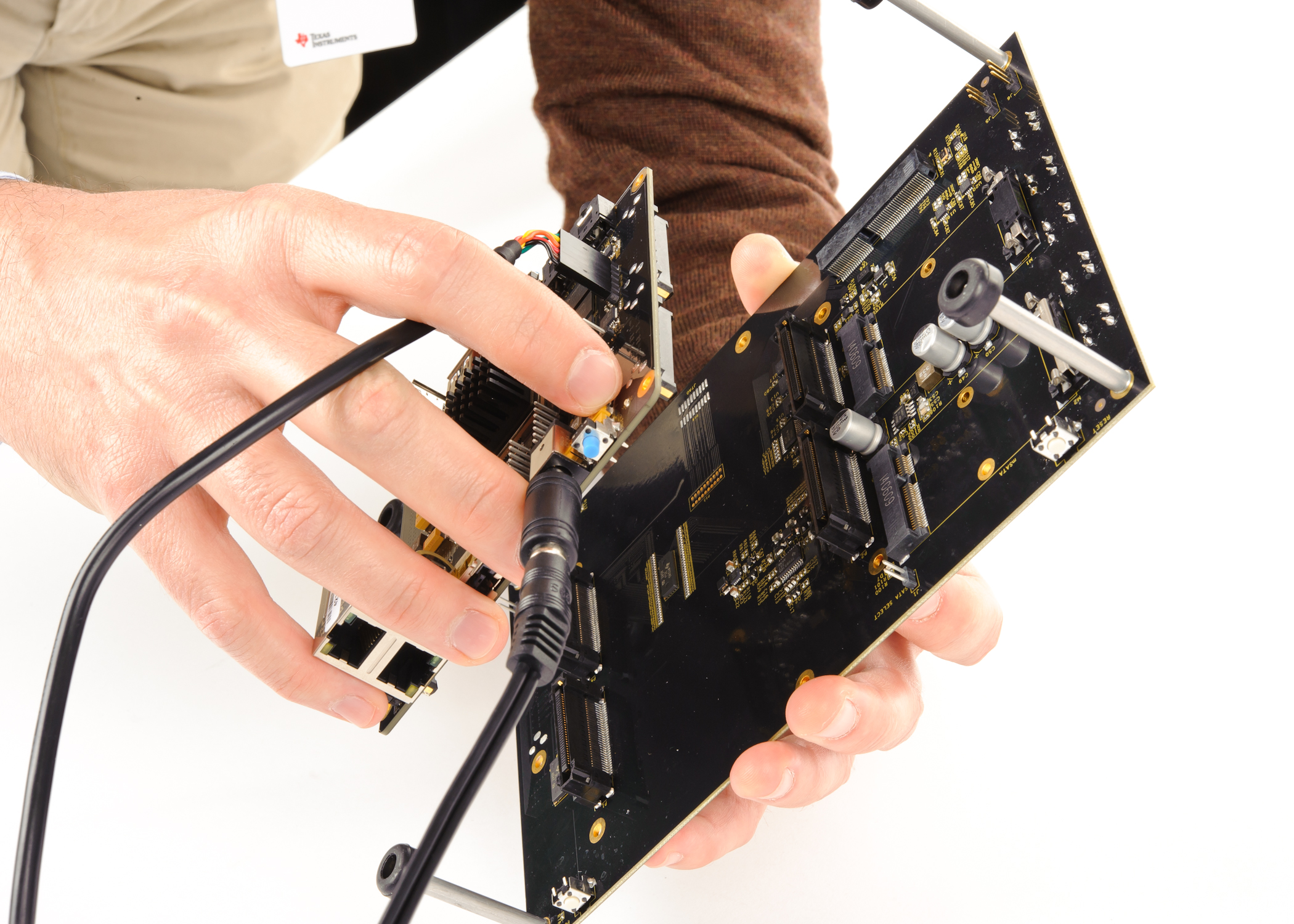
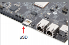
6.3.2. AM572x GP EVM Hardware Setup
Description
The AM572x Evaluation Module provides an affordable platform to quickly start evaluation of Sitara™ ARM® Cortex®-A15 AM57x Processors (AM5728, AM5726, AM5718, AM5716) and accelerate development for HMI, machine vision, networking, medical imaging and many other industrial applications. It is a development platform based on the dual ARM Cortex-A15, dual C66x DSP processor that is integrated with tons of connectivity such as PCIe, SATA, HDMI, USB 3.0/2.0, Dual Gigabit Ethernet, and more.
The AM572x Evaluation Module also integrates video and 3D/2D graphics acceleration, as well as a qual-core Programmable Real-time Unit (PRU) and dual ARM Cortex-M4 cores.
Contents of the kit
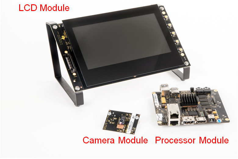
Module:
- Processor Module
- LCD Module
- Camera Module
Other components:
- µSD card with Linux SDK
- USB-to-serial debug cable
- HDMI cable for optional external display
- LCD brackets
Printed documentation:
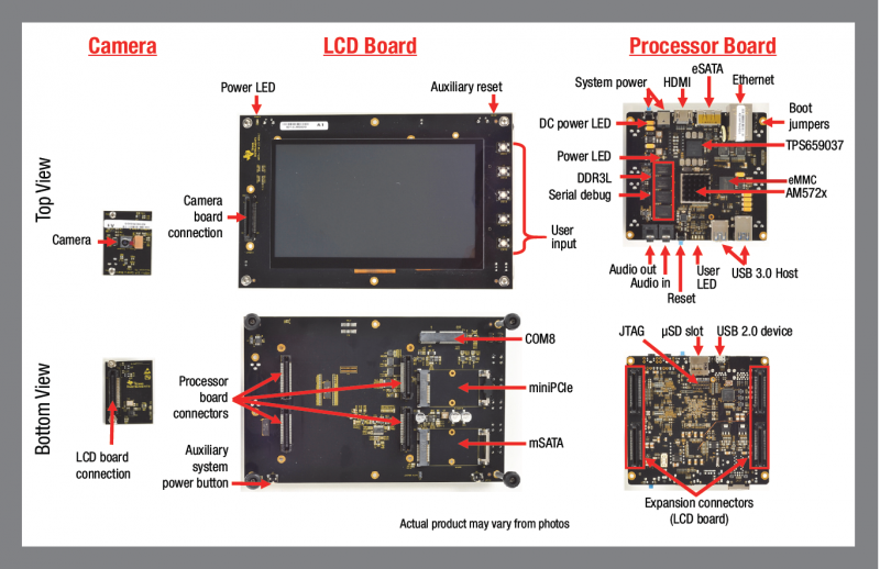
EVM Layout and Key Components
JTAG debug probes (aka Emulators) supported
List of standalone JTAG debug probes supported:
- XDS100-class JTAG debug probes (low cost, low performance). XDS100v1 is not supported.
- XDS200-class JTAG debug probes (recommended)
- XDS560v2-class JTAG debug probes (high performance)
Host Drivers
Download and install Virtual COM Port Drivers for TTL-232R-3V3 USB to UART cable from the FTDI website:
Minimal EVM setup
Setting boot switches
Other Boot Pin configurations: GP EVM Boot Options
Connecting Emulator
Note: This EVM setup is only required for developers who need to connect to cores using Code Composer studio to load application.
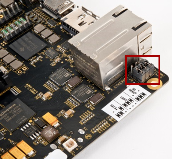
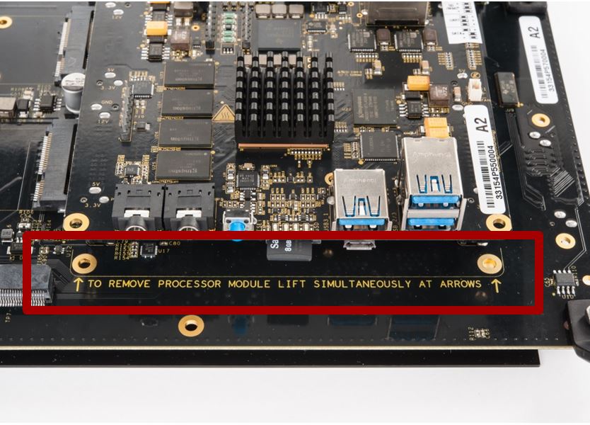
The JTAG emulation pins for the EVM are on the back of the processor module. User need to carefully unmount the processor module from the LCD panel in order to get access to the JTAG pins.
Refer to the image below for how to safely separate the processor module from the LCD panel.
|
|

Powering up the EVM
Power Supply specifications
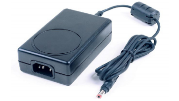
Please note that a power supply is NOT included with the AM572x Evaluation Module and needs to be purchased separately. A power supply with the following specs is needed:
- 12V DC output
- 5A output
- Positive inner and negative outer terminals
- Female barrel with 2.5mm inner diameter and 5.5mm outer diameter
- Isolated power supply
PMIC auto-off after seven seconds
The Power Management Integrated Circuit (PMIC) on the TMDSEVM572X turns off the board in seven seconds after power on to work around a hardware errata. After seven seconds, the PMIC powers off unless software writes to a PMIC register to keep it on.
In emulation setup, the GEL file will keep the PMIC on after you connect to the A15 core on the SoC. While booting from ROM bootloader user application software, would need to keep the PMIC ON while initializing the board.
In Linux boot, the uboot code keeps the PMIC On and in the TI RTOS boot scenario, the SBL component provides the same functionality
NOTE
- To allow quicker execution of the GEL before the PMIC shuts off, you can increase the JTAG TCLK Frequency in Advance settings of your target configuration to 15Mhz or to the maximum (20Mhz).
- If the above CCS connect sequence does not work in the first attempt, it means that the PMIC switched off before the GEL could initialize I2C and modify the PMIC settings. In that case, the connection has failed, hit connect in CCS debug view without removing the power cable and then immediately hit the power switch besides the power plug.
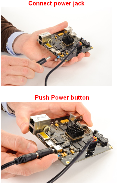
Connect Power to the EVM
CCS Setup
There are two scenarios while connecting to the EVM :
- Connect to EVM without a SD card boot image to boot the EVM
- Connect to EVM after booting an image from the SD card.
Connect without a SD card boot image
Configuring target configuration files
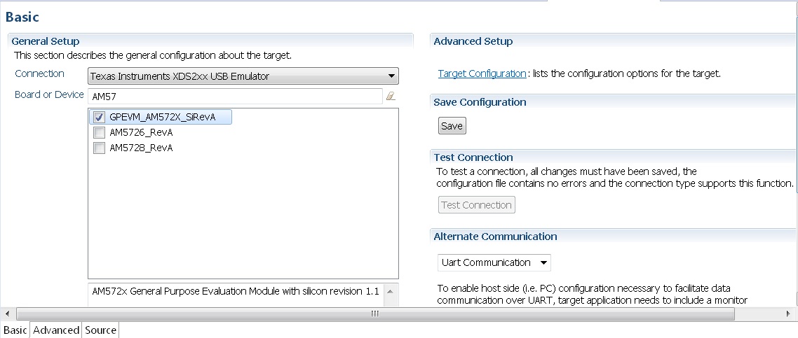
Launch CCS and create new target configuration(File->New->Target Configuration file) as shown in the images below and provide appropriate name to the configuration. Select Spectrum digital XDS200 emulator and target as GPEVM_AM572x_SiRevA.
Note: For older revisions of CCSv6, If you don`t find the GPEVM_AM572x_SiRevA target make sure you have installed the CCSv6 package with support for Sitara Processors and done the software update correctly from the Help Menu to get the latest Sitara CSP package.
In advance settings, make sure that the gel files are populated correctly. The following GEL files and their corresponding cores are provided below:
- IcePick_D: AM572x_ICEPickD_Utility.gel
- CS_DAP_DebugSS: AM572x_dap_startup.gel
- CS_DAP_PC: AM572x_CS_DAP_PC_Utility.gel
- A15_0: AM572x_cortexa15_cpu0_startup.gel
- A15_1: AM572x_cortexa15_cpu1_startup.gel
- C66x_0: AM572x_dsp_startup.gel
- C66x_1: AM572x_dsp_startup.gel
- M4_IPU_1_C0: AM572x_cortexM4_startup.gel
- M4_IPU_1_C1: AM572x_cortexM4_startup.gel
- M4_IPU_2_C0: AM572x_cortexM4_startup.gel
- M4_IPU_2_C1: AM572x_cortexM4_startup.gel
- IVAHD: AM572x_ivahd_startup.gel
Connecting to target
Step1 : Download Code composer Studio and AM572x Sitara CSP package as described in the wiki article mentioned below:
Install Code composer Studio v6 for AM572x
Step2: AM572x EVM doesn`t have any boot switches to configure for emulation mode. so configure the boot switches to SD Boot Mode. Dont Populate the uSD card when the intent is to connect and load code over emulator and not to boot the device using uSD card.
Step3: Connect an XDS200 Emulator to emulation pins at the back of the GP EVM as shown in section.Connecting_Emulator
Step4: Launch CCS and create new target configuration as discussed in the previous section.
IcePick_D: GEL Output: IVAHD ICONT1 is released from Wait-In-Reset.
IcePick_D: GEL Output: IVAHD ICONT2 is released from Wait-In-Reset.
CS_DAP_DebugSS: GEL Output: --->>> CONFIGURE DEBUG DPLL settings to 1.9 GHZs  <<<---
CS_DAP_DebugSS: GEL Output: > Setup DebugSS 1.9GHz in progress...
CS_DAP_DebugSS: GEL Output: < Done with Setup DebugSS Trace export clock (TPIU) to 97MHz
CS_DAP_DebugSS: GEL Output: < Done with Setup DebugSS PLL Clocking 1.9GHz
CS_DAP_DebugSS: GEL Output: < Done with Setup DebugSS ATB Clocking 380MHz
CS_DAP_DebugSS: GEL Output: < Done with Setup DebugSS Trace export clock (TPIU) to 97MHz
CS_DAP_DebugSS: GEL Output: --->>> TURNING ON L3_INSTR and L3_3 clocks required for debug instrumention <<<<<<----
CS_DAP_DebugSS: GEL Output: ---<<< L3 instrumentation clocks are enabled >>>> ---
CS_DAP_DebugSS: GEL Output: --->>> Mapping TIMER supsend sources to default cores <<<<<<----
CS_DAP_PC: GEL Output: Cortex-A15 1 is not in WIR mode so nothing to do.
CortexA15_0: GEL Output: --->>> AM572x GP EVM <<<---
CortexA15_0: GEL Output: --->>> AM572x Target Connect Sequence Begins ... <<<---
CortexA15_0: GEL Output: --->>> I2C Init <<<---
CortexA15_0: GEL Output: --->>> AM572x Begin MMC2 Pad Configuration <<<---
CortexA15_0: GEL Output: --->>> AM572x End MMC2 Pad Configuration <<<---
CortexA15_0: GEL Output: --->>> AM572x PG2.0 GP device <<<---
CortexA15_0: GEL Output: --->>> PRCM Clock Configuration for OPPNOM in progress... <<<---
CortexA15_0: GEL Output:    Cortex A15 DPLL OPP 0 clock config is in progress...
CortexA15_0: GEL Output:    Cortex A15 DPLL is already locked, now unlocking...
CortexA15_0: GEL Output:    Cortex A15 DPLL OPP 0 is DONE!
CortexA15_0: GEL Output:    IVA DPLL OPP 0 clock config is in progress...
CortexA15_0: GEL Output:    IVA DPLL OPP 0 is DONE!
CortexA15_0: GEL Output:    PER DPLL OPP 0 clock config in progress...
CortexA15_0: GEL Output:    PER DPLL already locked, now unlocking
CortexA15_0: GEL Output:    PER DPLL OPP 0 is DONE!
CortexA15_0: GEL Output:    CORE DPLL OPP 0 clock config is in progress...
CortexA15_0: GEL Output:    CORE DPLL OPP  already locked, now unlocking....
CortexA15_0: GEL Output:    CORE DPLL OPP 0 is DONE!
CortexA15_0: GEL Output:    ABE DPLL OPP 0 clock config in progress...
CortexA15_0: GEL Output:    ABE DPLL OPP 0 is DONE!
CortexA15_0: GEL Output:    GMAC DPLL OPP 0 clock config is in progress...
CortexA15_0: GEL Output:    GMAC DPLL OPP 0 is DONE!
CortexA15_0: GEL Output:    GPU DPLL OPP 0 clock config is in progress...
CortexA15_0: GEL Output:    GPU DPLL OPP 0 is DONE!
CortexA15_0: GEL Output:    DSP DPLL OPP 0 clock config is in progress...
CortexA15_0: GEL Output:    DSP DPLL OPP 0 is DONE!
CortexA15_0: GEL Output:    PCIE_REF DPLL OPP 0 clock config is in progress...
CortexA15_0: GEL Output:    PCIE_REF DPLL OPP 0 is DONE!
CortexA15_0: GEL Output: --->>> PRCM Clock Configuration for OPP 0 is DONE! <<<---
CortexA15_0: GEL Output: --->>> PRCM Configuration for all modules in progress... <<<---
CortexA15_0: GEL Output: --->>> PRCM Configuration for all modules is DONE! <<<---
CortexA15_0: GEL Output: --->>> DDR3 Initialization is in progress ... <<<---
CortexA15_0: GEL Output:    DDR DPLL clock config for 532MHz is in progress...
CortexA15_0: GEL Output:    DDR DPLL clock config for 532MHz is in DONE!
CortexA15_0: GEL Output:        Launch full leveling
CortexA15_0: GEL Output:        Updating slave ratios in PHY_STATUSx registers
CortexA15_0: GEL Output:        as per HW leveling output
CortexA15_0: GEL Output:        HW leveling is now disabled. Using slave ratios from
CortexA15_0: GEL Output:        PHY_STATUSx registers
CortexA15_0: GEL Output:        Two EMIFs in interleaved mode - (2GB total)
CortexA15_0: GEL Output: --->>> DDR3 Initialization is DONE! <<<---
CortexA15_0: GEL Output: --->>> AM572x Target Connect Sequence DONE !!!!!  <<<---
CortexA15_0: GEL Output: --->>> IPU1SS Initialization is in progress ... <<<---
CortexA15_0: GEL Output: --->>> IPU1SS Initialization is DONE! <<<---
CortexA15_0: GEL Output: --->>> IPU2SS Initialization is in progress ... <<<---
CortexA15_0: GEL Output: --->>> IPU2SS Initialization is DONE! <<<---
CortexA15_0: GEL Output: --->>> DSP1SS Initialization is in progress ... <<<---
CortexA15_0: GEL Output: DEBUG: Clock is active ...
CortexA15_0: GEL Output: DEBUG: Checking for data integrity in DSPSS L2RAM ...
CortexA15_0: GEL Output: DEBUG: Data integrity check in GEM L2RAM is sucessful!
CortexA15_0: GEL Output: --->>> DSP1SS Initialization is DONE! <<<---
CortexA15_0: GEL Output: >> START ==> Enable L3 Clk
CortexA15_0: GEL Output: >> Change Suspend source for GPTimer5 to DSP1
CortexA15_0: GEL Output: --->>> DSP2SS Initialization is in progress ... <<<---
CortexA15_0: GEL Output: DEBUG: Clock is active ...
CortexA15_0: GEL Output: DEBUG: Checking for data integrity in DSPSS L2RAM ...
CortexA15_0: GEL Output: DEBUG: Data integrity check in GEM L2RAM is sucessful!
CortexA15_0: GEL Output: --->>> DSP2SS Initialization is DONE! <<<---
CortexA15_0: GEL Output: --->>> IVAHD Initialization is in progress ... <<<---
CortexA15_0: GEL Output: DEBUG: Clock is active ...
CortexA15_0: GEL Output: --->>> IVAHD Initialization is DONE! ... <<<---
CortexA15_0: GEL Output: --->>> PRUSS 1 and 2 Initialization is in progress ... <<<---
CortexA15_0: GEL Output: --->>> PRUSS 1 and 2 Initialization is in complete ... <<<---
Multi-core Initialization
After connecting to the boot master core – typically the ARM core – you may need to connect to a slave core in order to run code. Depending on your SOC, the slave core can be
- DSP C66x
- ARM M4
- PRUSS
- IVAHD
Typically the slave cores will wait in reset state until the master core
wakes up the slave core to run code. To connect to the slave core on
AM57x, go to Scripts menu in CCS Debug View and under AM572x
MULTICORE Initialization enable the corresponding sub system clock.
For example, enable DSP11SSClkEnable_API for the first DSP core.
After running the clock enable option, you can connect to the core.
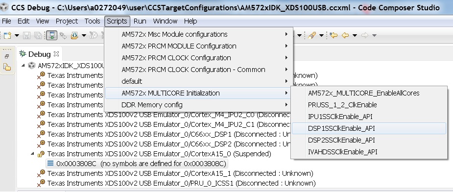
If you wish to run TI RTOS code on DSP, please also run the Timer Suspend Control Options.
Connect after booting from SD card
When you boot an image from the SD card, the secondary boot loader will configure the device clocks, DDR and wake up the slave cores on the AM572x processor on GP EVM hence you don`t need the GEL initialization scripts to redo the clock and DDR settings.
Note: If you are running the Image processing demo or have created an SD card with the SBL (mlo) for booting the board then please follow the following procedure
Configuring target configuration files
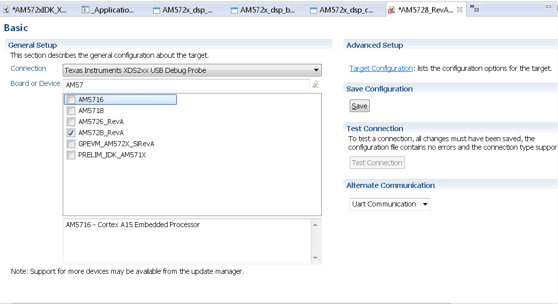
Launch CCS and create new target configuration(File->New->Target Configuration file) as shown in the images below and provide appropriate name to the configuration. Select Spectrum digital XDS200 emulator and target as AM5728_RevA. This target setting will not populate the GEL files when you connect to the target
Note: If you don`t find the AM572x_RevA target make sure you have installed the CCSv6.1.1 package and done the software update correctly.
GEL file options
Changing SoC Operating point
The GEL file for setting the clocks on the SoC provides 3 Operating points OPP_NOM, OPP_OD and OPP_HIGH.
OPP_NOM PLL Settings:
- ARM = 1000 MHz
- DSP = 600 Mhz
- IVA = 532 Mhz
OPP_OD PLL Settings:
- ARM = 1176 MHz
- DSP = 600 Mhz
- IVA = 430 Mhz
- GPU =500 Mhz
OPP_HIGH PLL Settings:
- ARM = 1500 MHz
- DSP = 700 Mhz
- GPU = 425 Mhz
- IVA = 388.3 Mhz
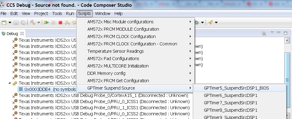
Timer Suspend Control Options for DSP
On AM57xx devices, all the timers on the chip have their suspend control signal routed to the A15 core. Which means that if any of the slave cores are using these timers, the timers will continue to run even when the slave core has been paused. The timer will only pause when the A15 core is halted.
This is confusing while debugging code on slave cores if you are relying on timer for logging, inserting delays or if the timer keeps firing interrupts even when the core is halted. One such scenario occurs with GPtimer5 when DSP developers are using SYS/BIOS. The OS uses GPtimer5 on the DSP and forces a frequency check to confirm the timer configuration, however the OS can’t gain access to the timer due to the hook up of the suspend control signals.
Due to this issue the SYS/BIOS developers will need to configure an additional CCS configuration check to connect the GPTimer suspend control signal to the DSP as shown in the image below:
Other How-To Options
Connecting the UART
Connecting FTDI cable to the 6 pin UART header for serial debug

Note: Pin 1 corresponds to ground.
Connect the USB end to the host. If you connect to the EVM UART, use the following host configuration setup in the serial terminal software (Minicom, Teraterm, etc) Baud Rate: 115200 Data Bits: 8 Parity: None Flow Control: Off
Connect Ethernet cable to enable Network Connectivity
For ethernet connectivity connect the ethernet cable to the top serial port which is port 0 on the GP EVM.

You can connect the other end of the cable directly to the host or through a network switch based on the configuration required for your test setup.
6.3.3. TMDXIDK5728 Hardware Setup
Description
The TMDXIDK5728 is a standalone test, development, and evaluation module system that enables developers to write software and develop hardware for industrial communication type applications. It has been equipped with a TI AM572x processor and a defined set of features to allow the user to experience industrial communication solutions using serial or Ethernet based interfaces. Using standard interfaces, the IDK may interface to other processors or systems and act as a communication gateway in this case. In addition it can directly operate as a standard remote I/O system or simple sensor connected to an industrial communication network. The embedded emulation logic allows emulation and debug using standard development tools such as TI’s Code Composer Studio by just using the supplied USB cable.
EVM Layout and key components
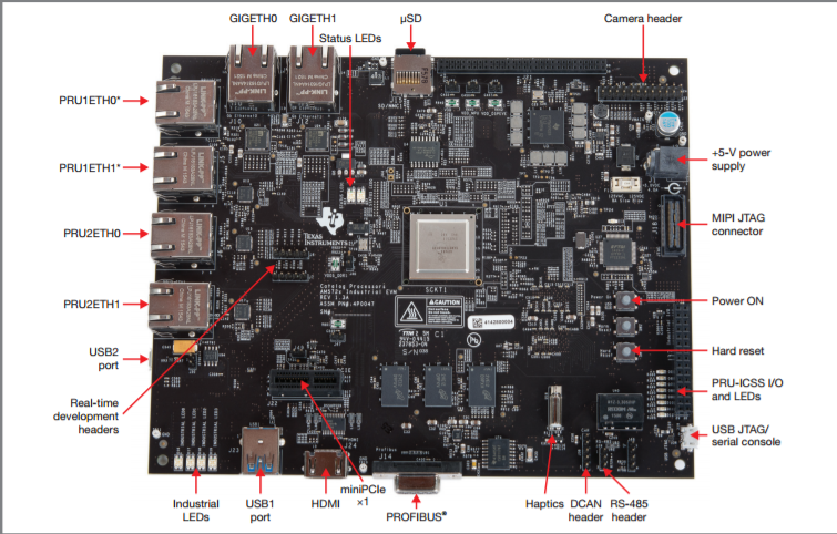
- PRU1ETH0 and PRU2ETH0 are not enabled by default
Quick Start Guide
This section talks about how to quickly setup the AM572x Industrial Development Kit (IDK) EVM. This guide is a Beta version and it is designed to help you through the initial setup of the EVM.
| 1. Once you have received the TI-RTOS or Linux™ software from your TI representative, create a bootable µSD card (using the included blank µSD) and insert it into the EVM |
|
| 2. Connect the power cable to the power jack on the board and plug in to an AC power source |
|
Note: When powering this IDK, always use the recommended power supply (GlobTek Part Number TR9CA6500LCP-N, Model Number GT-43008-3306-1.0-T3) or equivalent model having output voltage of +5VDC and output current max 6.5 Amp as well as the applicable regional product regulatory/safety certification requirements requirements such as (by example) UL, CSA, VDE, CCC, PSE, etc.
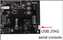
| 3. Connect the microUSB cable to USB JTAG/Console port on the EVM and connect to the USB on the host. Connect Ethernet cable to GIG ETH0 if Network connectivity is required |
|
Note: The serial port will not show up on the host PC until you power on the EVM.
| 4. Select the power ON button to run power the IDK. |
|
After, you power on the EVM the Status, Industrial LED2, Industrial LED3 will turn on. If the microUSB cable is pluged in then the LED corresponding to FTDI UARTtoUSB will be turned on.
| 5. Users can now connect to UART and the on board XDS100 emulator from the host machine.For UART port connections set the serial terminal software Tera term/minicom/hyperterminal to baudrate 115200 to see log messages. Connecting to target using emulator has been discussed in the section below. | |
|
|
Connecting IDK EVM to Code Composer Studio
Step1 : Download Code composer Studio and AM572x Sitara CSP package as described in the wiki article mentioned below:
Install Code composer Studio for AM572x
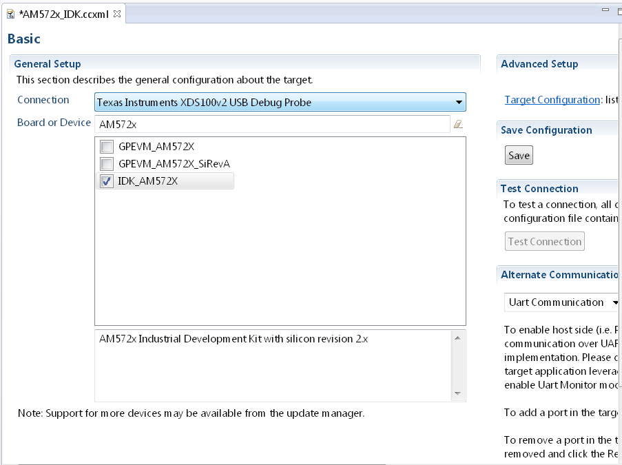
Step2: Connect IDK EVM as described in the Quick Start Guide. Populating the uSD card is not required as the intent is to connect and load code over emulator and not to boot the device using uSD card. AM572x IDK doesn`t have any boot switches to configure for emulation mode.
Step3: Launch CCS and create new target configuration(File->New->Target Configuration file) as shown in the images below and provide appropriate name to the configuration. Select Texas Instuments XDS100v2 emulator and target as IDK_AM572x.
NOTE If you don`t find the IDK_AM572x target make sure you have installed the Sitara Device support version 1.3.x package correctly
- Cortex_A15_0: ..\..\emulation\boards\am572x\gel\idk_am572x.gel
- C66x_DSP1: ..\..\emulation\boards\am572x\gel\AM572x_dsp_startup.gel
- Cortex_M4_IPU1_C0: ..\..\emulation\boards\am572x\gel\AM572x_cortexM4_startup.gel
Note: GEL files are located under ccsv6\ccs_base\emulation\boards\am572x\gel after the CSP package is installed
CortexA15_0: GEL Output: --->>> AM572x Target Connect Sequence Begins ... <<<---
CortexA15_0: GEL Output: --->>> AM572x Begin MMC2 Pad Configuration <<<---
CortexA15_0: GEL Output: --->>> AM572x End MMC2 Pad Configuration <<<---
CortexA15_0: GEL Output: --->>> AM572x PG1.1 GP device <<<---
CortexA15_0: GEL Output: --->>> I2C Init <<<---
CortexA15_0: GEL Output: --->>> PRCM Clock Configuration for OPPNOM in progress... <<<---
CortexA15_0: GEL Output:    Cortex A15 DPLL OPP 0 clock config is in progress...
CortexA15_0: GEL Output:    Cortex A15 DPLL is already locked, now unlocking...
CortexA15_0: GEL Output:    Cortex A15 DPLL OPP 0 is DONE!
CortexA15_0: GEL Output:    IVA DPLL OPP 0 clock config is in progress...
CortexA15_0: GEL Output:    IVA DPLL OPP 0 is DONE!
CortexA15_0: GEL Output:    PER DPLL OPP 0 clock config in progress...
CortexA15_0: GEL Output:    PER DPLL already locked, now unlocking
CortexA15_0: GEL Output:    PER DPLL OPP 0 is DONE!
CortexA15_0: GEL Output:    CORE DPLL OPP 0 clock config is in progress...
CortexA15_0: GEL Output:    CORE DPLL OPP  already locked, now unlocking....
CortexA15_0: GEL Output:    CORE DPLL OPP 0 is DONE!
CortexA15_0: GEL Output:    ABE DPLL OPP 0 clock config in progress...
CortexA15_0: GEL Output:    ABE DPLL OPP 0 is DONE!
CortexA15_0: GEL Output:    GMAC DPLL OPP 0 clock config is in progress...
CortexA15_0: GEL Output:    GMAC DPLL OPP 0 is DONE!
CortexA15_0: GEL Output:    GPU DPLL OPP 0 clock config is in progress...
CortexA15_0: GEL Output:    GPU DPLL OPP 0 is DONE!
CortexA15_0: GEL Output:    DSP DPLL OPP 0 clock config is in progress...
CortexA15_0: GEL Output:    DSP DPLL OPP 0 is DONE!
CortexA15_0: GEL Output:    PCIE_REF DPLL OPP 0 clock config is in progress...
CortexA15_0: GEL Output:    PCIE_REF DPLL OPP 0 is DONE!
CortexA15_0: GEL Output: --->>> PRCM Clock Configuration for OPP 0 is DONE! <<<---
CortexA15_0: GEL Output: --->>> PRCM Configuration for all modules in progress... <<<---
CortexA15_0: GEL Output: --->>> PRCM Configuration for all modules is DONE! <<<---
CortexA15_0: GEL Output: --->>> DDR3 Initialization is in progress ... <<<---
CortexA15_0: GEL Output:    DDR DPLL clock config for 532MHz is in progress...
CortexA15_0: GEL Output:    DDR DPLL clock config for 532MHz is in DONE!
CortexA15_0: GEL Output: DEBUG: Overall DDR configuration
CortexA15_0: GEL Output: DEBUG: EMIF1 and EMIF1 DDR IOs config (CTRL_MODULE_CORE_PAD module)
CortexA15_0: GEL Output: DEBUG: DDR PHY config (CTRL_MODULE_WKUP module)
CortexA15_0: GEL Output: DEBUG: EMIF1 ctrl + associated DDR PHYs initial config (EMIF1 module)
CortexA15_0: GEL Output: DEBUG: EMIF1 channel - Launch full levelling
CortexA15_0: GEL Output: DEBUG: EMIF2 ctrl + associated DDR PHYs initial config (EMIF2 module)
CortexA15_0: GEL Output: DEBUG: EMIF1 channel - Launch full levelling
CortexA15_0: GEL Output: DEBUG: Setting LISA maps in non-interleaved dual-EMIF mode
CortexA15_0: GEL Output: --->>> DDR3 Initialization is DONE! <<<---
CortexA15_0: GEL Output: --->>> AM572x Target Connect Sequence DONE !!!!!  <<<
Step6 : To connect to the DSP, M4,PRUSS or to IVAHD go to Scripts menu and under AM572x MULTICORE Initialization enable the corresponding Sub system clock Enable API.For Eg. FOr DSP1 select DSP11SSClkEnable_API. After running the clock enable option, you can connect to the core.
6.3.4. 66AK2GX GP EVM Hardware Setup
Description
The EVMK2G is a high performance, cost-efficient, standalone development platform that enables users to evaluate and develop applications for the Texas Instrument’s Keystone2 System-on-Chip (SoC) 66AK2GX. The Key features of EVM are:
Processor and controller
- K2G SoC 66AK2GX is based on keystone II architecture with ARM cortex A15 @600MHz and C66x DSP @600MHz
- Board Management Controller (BMC) for board management functions like system status and Boot mode control
Volatile and non volatile Memory/Interfaces:
- 2GByte of DDR3L with ECC
- 2Gbit of NAND Flash
- 128Mbit of SPI Flash
- 512Mbit of QSPI Flash
- 128kByte of I2C EEPROM for Boot support from I2C
- Micro SD-Card slot
- 16GByte of eMMC
High speed and Serial Interfaces
- Gigabit Ethernet port supporting 10/100/1000 Mbps data rate on RJ45 connector
- PCIe x1 card slot
- COM8 interface
- DCAN and MLB interfaces
- One USB2.0 host and one USB2.0 Dual-role ports
- One RS232 serial interface on DB9 connector or UART over mini-USB connector, One UART interface on 6 pin header
Multimedia and display:
- 4.3” LCD display with Capacitive touch (Sold separately)
- HDMI transmitter
- Audio Line In and Line Out
JTAG and Emulation:
- MIPI 60-Pin JTAG header to support all types of external emulator
- On Board XDS200 Emulator
- Powered by DC power-wall adaptor (12V/5A)
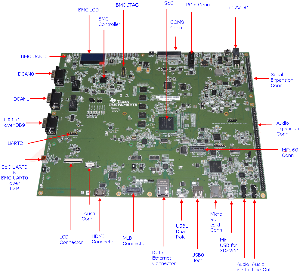
EVM Layout and Key Components
JTAG debug probes (aka Emulators) supported
List of standalone JTAG debug probes supported:
- XDS100-class JTAG debug probes (low cost, low performance). XDS100v1 is not supported.
- XDS200-class JTAG debug probes (recommended)
- XDS560v2-class JTAG debug probes (high performance)
Minimal EVM setup
Setting boot switches
The DIP Switch /Boot mode switch (SW3) is used for selecting the boot mode.

Note: Read the PCB marking around the boot switch for your EVM to interpret of ON and OFF marking on the switch
- For Rev C K2G02 GP EVM: ON = ‘0’ and OFF = ‘1’
- For Rev C/Rev D K2G12 GP EVM: ON = ‘1’ and OFF = ‘0’
Other Boot Pin configurations:
| SW3[4:1] | BOOT MODE |
|---|---|
| 0000 (0x0) | Sleep/No Boot |
| 0001 (0x1) | PCIe boot |
| 0010 (0x2) | Ethernet Boot |
| 0011 (0x3) | I2C PLL Boot |
| 0100 (0x4) | SPI No PLL Boot |
| 0101 (0x5) | SPI PLL-1 Boot |
| 0110 (0x6) | USB Boot |
| 0111 (0x7) | MMC/SD Boot |
| 1000 (0x8) | UART Boot |
| 1001 (0x9) | QSPI 96 Boot |
| 1010 (0xa) | eMMC Boot |
| 1011 (0xb) | NAND Boot |
| 1100 (0xc) | I2C No PLL Boot |
| 1101 (0xd) | SPI PLL-2 Boot |
| 1110 (0xe) | SPI PLL-3 Boot |
| 1111 (0xf) | QSPI 48 Boot |
Connecting Emulator
Note: This EVM setup is only required for developers who need to connect to cores using Code Composer studio to load application.
When external emulator is not connected to MIPI 60-pin connector, On-board XDS200 embedded JTAG emulator is the default type of emulation (SoC JTAG signals are routed to XDS200 on-board emulator). When external emulator is connected to MIPI 60-pin header, it is automatically detected and SoC JTAG signals are routed to external emulator.
On Board XDS200 emulator
EVMK2G has on-board XDS200 embedded JTAG emulation circuitry. Hence user does not require any external emulator to connect EVM with Code Composer Studio (CCS). User can connect target SoC in EVM to CCS through USB cable supplied in the EVM kit.
Use the USB to USB mini-B cable provided. Connect the USB mini-B connector to the USB mini-B interface near to the audio line in on the EVM, and the USB connector to your PC. This enables XDS-2xx emulation and is directly useable by CCS.
NOTE On Rev C boards and earlier revisions of the board, users who plan to connect the USB cable to USB 3.0 cable need to follow the instructions to update Emulation firmware using steps described in the article Updating_the_XDS200_firmware Without the firmware update, users are recommended to disconnect the mini USB cable from the XDS USB connector before powering up the EVM and reconnect after board power up is complete.
If you are using a different JTAG, you can connect it at MIPI60 connector (EMU1). The MIPI 60-pin JTAG header is provided on-board for high speed real-time emulation. All JTAG and EMUxx signals are terminated on MIPI 60-pin header.
No emulation firmware upgrade is required if users plan to use an external emulator The MIPI 60-pin JTAG header supports all standard (XDS510 or XDS560) TI DSP emulators. Please refer to the documentation supplied with your emulator for connection assistance.
Powering up the EVM
Power Supply specifications
The EVMK2G can be powered from a single +12V / 5.0A DC (60W) external power supply connected to the DC power jack (J3). Internally, +12V input is converted into required voltage levels using local DC-DC converters
Please note that a power supply is included with the 66AK2GX Evaluation Module. The power supply has the following specs :
- 12V DC output
- 5A output
- Positive inner and negative outer terminals
- Female barrel with 2.5mm inner diameter and 5.5mm outer diameter
- Isolated power supply
CCS Setup
This section describes the setup to connect to 66AK2GX GP EVM using Code composer Studio environment and an emulator.
There are two scenarios while connecting to the EVM :
- Connect to EVM without a SD card boot image to boot the EVM
- Connect to EVM after booting an image from the SD card.
Before discussing both these scenarios, let us look at how to pull in the latest KeystoneII device support in CCSv6
Update CCS v6 to install Keystone II device Support package
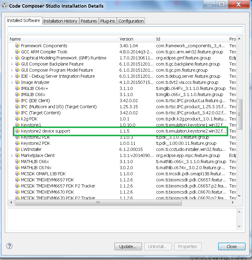
All revisions of the board require this step to be performed in order to get the latest GEL files and the target content for the K2G. This step will not be required for CCS versions higher than version 6.1.3. CCSv6.1.3 package contain KeystoneII device support package v1.1.4 which doesn`t contain 66AK2GX GPEVM specific target files hence we recommend this update.
Step 1 All CCS v6.1.3 and earlier version users are required to update the Keystone Device Support package by going into the Help->Check For Updates
Step 2 Select Keystone2 device support package. Follow menu options to continue with the update
Step 3 After the update is complete go to Help->Installation details and check that Keystone2 device support package v1.1.5 or later are installed as shown below
Note: The package can be downloaded separately from the link below and manually unzipped into CCSv6 installation.
Connect without a SD card boot image
Configuring target configuration files
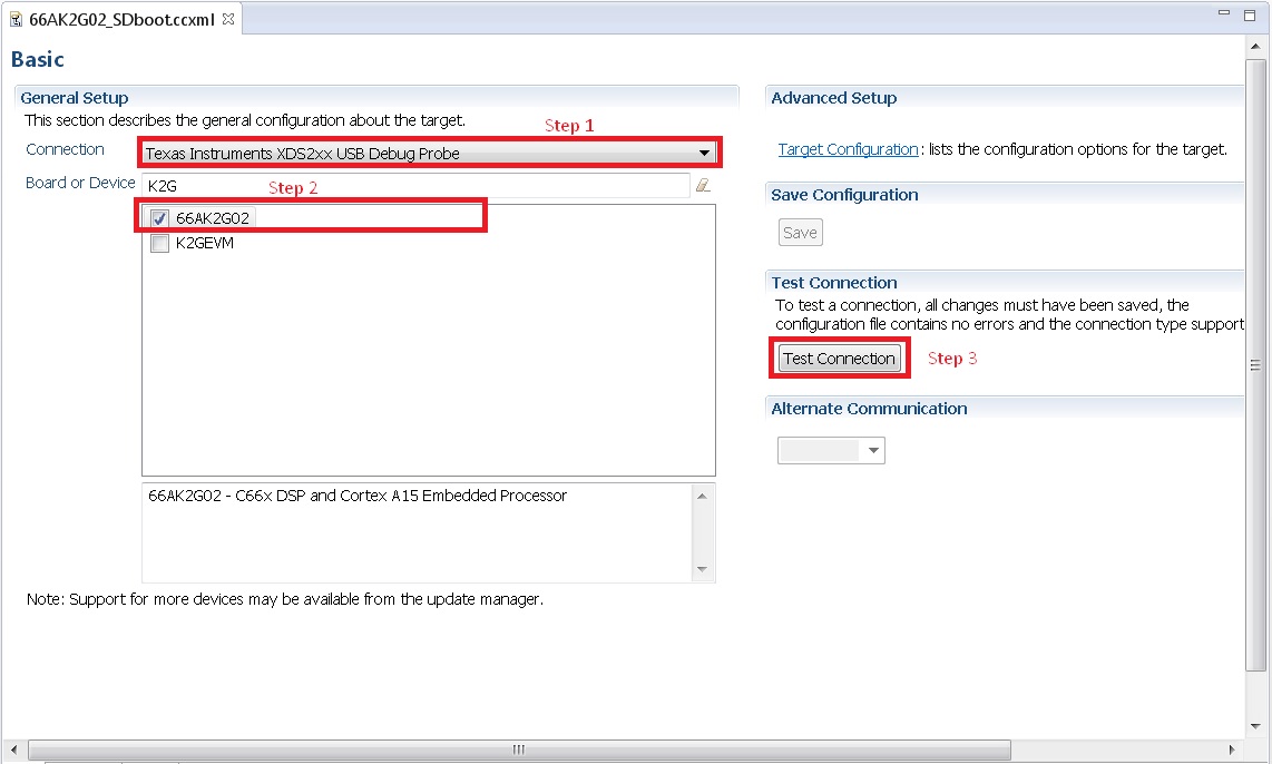
Launch CCS and create new target configuration(File->New->Target Configuration file) as shown in the images below
Provide appropriate name to the configuration. Select Spectrum digital XDS200 emulator and target as K2G GPEVM.
Note: If you don`t find the 66AK2G02 target make sure you have installed the CCSv6.1.3 package or for CCSv6.1.2 and earlier ensure that you have done the software update correctly as shown in the how to section below.
In advance settings, make sure that the gel files are populated correctly. The following GEL files and their corresponding cores are provided below:
- C66X Core: evmk2g.gel
- A15 Core: evmk2g_arm.gel
Connecting to target
Step1 : Download Code composer Studio v6.1.3 or for CCSv6.1.2 and earlier, ensure it contains Keystone device support package version 1.1.5 as described in the how to guide
Install Code composer Studio v6 for K2G
- Step2: 66AK2GX GP EVM contains boot switches to configure for “No
- boot/sleep” mode. So configure the boot switches to No Boot Mode as described in the SettingBootSwitches
Step3: Connect an XDS200 Emulator to XDS USB of the GP EVM as shown in ConnectingEmulator
Step4: Launch CCS and create new target configuration as discussed in the previous section ConfiguringTargetConfigFile
Step5: Launch Target configuration you just created.
- Step6:K2G can be a DSP or an ARM master boot device so connect to
- the C66x or the A15_0.
GEL Log
A15_0: GEL Output: PLL has been configured (24.0 MHz * 100 / 1 / 4 = 600.0 MHz)
A15_0: GEL Output: ARM PLL has been configured with ref clock 24MHz, -sysclkp_period 41.6666 (24.0 MHz * 100 / 1 / 4 = 600.0 MHz)
A15_0: GEL Output: Power on all PSC modules and DSP domains...
A15_0: GEL Output: Power on PCIE PSC modules and DSP domains... Done.
A15_0: GEL Output: UART PLL has been configured (24.0 MHz * 128 / 1 / 8 = 384.0 MHz)
A15_0: GEL Output: NSS PLL has been configured (24.0 MHz * 250 / 3 / 2 = 1000.0 MHz)
A15_0: GEL Output: ICSS PLL has been configured (24.0 MHz * 250 / 3 / 10 = 200.0 MHz)
A15_0: GEL Output: DSS PLL has been configured (24.0 MHz * 198 / 12 / 16 = 24.75 MHz)
A15_0: GEL Output: DDR PLL has been configured (24.0 MHz * 250 / 3 / 10 = 200.0 MHz)
A15_0: GEL Output: XMC setup complete. A15_0: GEL Output: DDR3 PLL Setup ...
A15_0: GEL Output: DDR3 PLL Setup complete, DDR3A clock now running at 400MHz.
A15_0: GEL Output: DDR3A initialization complete
Connect with a SD card boot image
Launch CCS and create new target configuration(File->New->Target Configuration file) as shown in the images below
Provide appropriate name to the configuration. Select Spectrum digital XDS200 emulator and target as 66AK2G02.
Note: If you don`t find the 66AK2G02 target make sure you have installed the CCSv6.1.3 package or for CCSv6.1.2 and earlier ensure that you have done the software update correctly as shown in the how to section below.
In advance settings, make sure that the no gel files are populated.
Step2: 66AK2G02 GP EVM contains boot switches to configure for “SD/MMC boot” mode. So configure the boot switches to SD/MMC boot Mode as described in the SettingBootSwitches
Step3: Connect an XDS200 Emulator to XDS USB of the GP EVM as shown in section ConnectingEmulator
Step4: Launch CCS and create new target configuration as discussed in the previous section ConfiguringTargetConfigFile
Step5: Launch Target configuration you just created.
Step6:K2G will boot with ARM master boot from the SD card so connect to the A15_0. There will be no output on the console when you connect to the core.
Step7 SD card boot image will typically load a secondary bootloader like u-boot that will put the DSP in reset so user will need to follow the instructions on the page that talks about Taking DSP out of reset
Note: RTOS users don`t need to follow this step as the Secondary bootloader (SBL) will put the DSP in idle state and not in reset if there is no code running on the DSP.
How to guide
This section guides users who are using older versions of the GP EVM which may require an update to the firmware flashed on the EVM or hardware updates to workaround specific issues. Each section specifies the affected versions and the fix for the issue.
Create SD card to boot Linux on the GP EVM
All pre-production boards (Rev C and earlier) will not contain a SD card image in the kit without an image flashed on it for the Out of Box experience described in the Quick start guide. User are required to download the image seperately from the Processor SDK Linux portal and run a script to create the SD boot image. The steps to create the image are provided below:
Step 1 Download the image k2g-evm-linux-xx.xx.xx.xx.img.zip from the link Latest Processor SDK Linux
Step 2 Follow instructions to create a SD card for the EVM using the instruction in the SD Card Creation Guide
Update the BMC firmware on the EVM
The section describes how the Board Management controller firmware on the board can be updated through the BMC UART interface. All boards prior to RevC, require a BMC update for the following issue:
- CDCM chip on the board generates clocks to modules like PCIe and USB. It is possible to use PCIe only in external clock mode on the EVM. However there can be use-cases where PCIe clock should be enabled with SoC running in internal clock mode.
Step 1 Install the LM flash programmer from link provided below:
Step 2 Obtain latest BMC software for the K2G GP EVM can be obtained from the board manufacturer or from local TI contact. Production EVMs are shipped with latest BMC version 0.6.1.0. You can check the version of the BMC software by observing the version indicated on BMC LCD on the GP EVM after power up.
Step 3 Connect the mini USB cable between host PC and ‘USB to SoC UART0’ port (J23) on EVM
Step 4 Remove the jumper J10 and power on the K2G EVM
Step 5 Open the LM Flash programmer utility on the windows host machine.
Step 6 In the LM Flash Programmer Utility ‘Configuration’ tab, in the interface section, select ‘Serial (UART)’ from the drop-down box on the left.Refer to the image provided below:
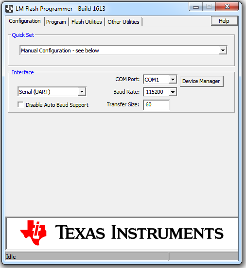
Step 7 Select the BMC COM Port and set the ‘Baud Rate’ to 115200.
- There will be two COM ports that appears on EVMs ‘USB to SoC UART0’ port. Select the one which is connected to BMC. To find which port corresponds to the BMC, you can open a serial terminal program or Device Manager on your PC and check the port number corresponding to “Silicon Labs CP210x: USB to UART Bridge: Standard COM Port (COM##)” as shown below:
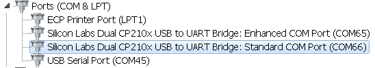
Note: BMC outputs boot logs to serial console when EVM is powered ON. Connect the ‘USB to SoC UART0’ port to standard serial console application to find the right COM port that is connected to BMC.
Step 8 Set ‘Transfer Size’ to 60, and make sure ‘Disable Auto Baud Support’ is unchecked.
Step 9 In the ‘Program’ tab, select the binary image file bmc_evmKS2_K2G.bin in the section ‘Select.bin file’.
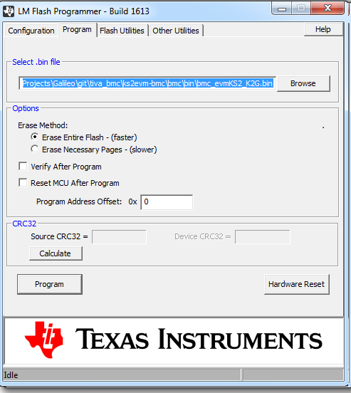
Step 10 Leave all other options as default, and press the ‘Program’ button.
Step 11 Wait till ‘Program Complete’ status in the status bar.
Step 12 Connect the jumper J10 and reboot the EVM
Update XDS200 firmware and hardware components on the GP EVM
Note: This update is only required if you are using the on board XDS200 debug probe.
The RevB and RevC boards are using an earlier version of the XDS200 firmware. We have observed the following issues when hooking up the internal XDS200 USB debug probe to a host machine.
- XDS200 Emulator USB cable need to be re-plugged every time board is power cycled/reset to avoid leakage on power supply VCC1V8_XDS which can damage the regulator or other ICs
Workaround for this issue
- Use external emulators with the MIPI 60 adapter included int he kit.
- Perform following firmware and hardware updates to the GP EVM (RevC and earlier)
Software Update Required
Steps to update the XDS200 firmware on the EVM are archived on the article Updating_the_XDS200_firmware
Hardware updates required
- Replace R431 & R442 to 200E
- Mount resistors R95, R107, R108, R115.
- Mount D2, R600, R599 components.
- Remove FB3 and connect a wire from R64.2 ‘rVCC_VBUS_XDS’ and R67.2 ‘VCC5V0_DCDC’ as shown in the image below:

Update the EVM for improved USB performance
The external resistors for the USB (R442 and R431) are currently 10k Ω. We recommend that users need to replace these with 200 Ω / 1%.
Useful Resources and Support
6.3.5. EVMK2E Hardware Setup Guide
6.3.5.1. Hardware Setup
Note
The EVM board is sensitive to electrostatic discharges (ESD). Use a grounding strap or other device to prevent damaging the board. Be sure to connect communication cables before applying power to any equipment.
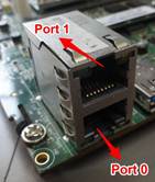
6.3.5.1.1. Attach the Ethernet cable
Using the Ethernet cable supplied, connect one end of the cable to the Ethernet Port 0 (At bottom one) on the EVM and the other end to your PC. The below picture shows which Ethernet Port is port 0:
6.3.5.1.2. Connect the JTAG interface
Use the USB to USB mini-B cable provided. Connect the USB mini-B connector to the USB mini-B interface near to the RST_PWR1 (Red color) button on the EVM, and the USB connector to your PC. This enables XDS-2xx emulation and is directly useable by CCS. If you are using a different JTAG, you can connect it at MIPI60 connector (EMU1).
6.3.5.1.3. K2E Set the boot mode switch SW1
K2E SPI Little Endian Boot mode (Default factory setting)
MSB                         LSB
SW1 - 1(OFF) 2(OFF) 3(ON) 4(OFF)
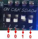
Note
Here a switch on “ON” position should be considered as “1”.
K2E No Boot/JTAG DSP Little Endian Boot mode
MSB                      LSB
SW1 - 1(ON) 2(ON) 3(ON) 4(ON)
6.3.5.1.4. Attach the serial port cable to the SoC UART port
Connect the SoC UART port to PC using the serial cable provided with the EVM. The SoC UART port is the 4-pin white connector COM1 of the EVM.
Start TeraTerm or HyperTerminal and set configuration to
- Baud Rate or Bits per second: 115200
- Data Bits: 8
- Parity: None
- Stop Bits: 1
- Flow Control: None
6.3.5.1.5. Connect the power cable
Connect the power cable to the EVM power jack on the board. To be ESD safe, plug in the other end of the power cable only after you have connected the power cord to the board. Then turn on the board.
6.3.5.2. DIP Switch and Bootmode Configurations
EVM SW1 switch Bootmode Configuration
The table below shows the bootmode combinations for the BMC v1.1.0.x. and value selected from internal flash memory of LM3s2d93.
| DIP Switch settings Selected | High_value of that bootmode | Low_value of that bootmode | Selected bootmode |
| 0000 | 0x00000000 | 0x00010067 | ARM NAND |
| 0001 | 0X00000000 | 0x00100001 | DSP No Boot |
| 0010 | 0x00000000 | 0x00008005 | ARM SPI |
| 0011 | 0x00000000 | 0x00100003 | ARM I2C Master |
| 0100 | 0x00000000 | 0x0000006F | ARM UART Master |
| 0101 | 0x00000000 | 0x0001506B | ARM RBL EthNet |
| 0110 | 0x00000000 | 0x00001061 | Sleep with Max PLL and ARM Bypass |
| 0111 | 0x00000000 | 0x00001061 | Sleep with Max PLL |
| 1000 | 0x00000000 | 0x00010167 | DSP NAND |
| 1001 | 0x00000000 | 0x00001061 | Sleep with Slow PLL and ARM Bypass |
| 1010 | 0x00000000 | 0x00008105 | DSP SPI-boot |
| 1011 | 0x00000000 | 0x00100103 | ARM I2C Master |
| 1100 | 0x00000000 | 0x0000016F | DSP UART boot |
| 1101 | 0x00000000 | 0x0001516B | DSP RBL ENET |
| 1110 | 0x00000000 | 0x00003661 | Sleep with Slow PLL and Slow ARM PLL |
| 1111 | 0x00000000 | 0x00100001 | DSP No-Boot |
6.3.5.3. EVM K2E How To Guides
6.3.5.3.1. Host driver for on-board mini-USB connector
The K2E EVM has a CP2105 device on-board. A driver must be installed on the host PC in order to be able to communicate with the EVM using the CP2105 mini-USB connector located at the corner edge of the EVM. The driver can be downloaded from CP2105 driver download.
Both Linux and Windows host machine drivers can be downloaded from this page. For Linux host machine, please follow the instructions given in the release notes. There are two versions of drivers for Linux kernel version 3.x.x and 2.6.x. Please download appropriate drivers after identifying the correct kernel version of the user’s host machine.
Note
Before testing the USB connection, make sure that the mini-USB cable is plugged into the port on the base board.
After installing the driver and connecting the USB cable, two COM ports should be visible in the list of COM ports available to connect to in the PC Host terminal console. The lower COM port (Enhanced) corresponds to the SoC UART and the higher (Standard) one corresponds to the MCU UART.
6.3.5.3.2. BMC Version Check and Update
BMC, or Board Management Controller, takes care of the power, clocks, resets, bootmodes, etc. of the EVM.
You can check the version by:
- Opening a hyperterminal or another similar type of console application.
- Set COM Port to higher value.
- When you connect to CP2105 mini-USB on the EVM it will provide two COM port connections, one to the SOC UART and one to BMC UART.
- The SOC UART will always be the “Enhanced” COM port, for example COM6 (actual COM PORT values will vary.)
- Set COM port properties appropriately:
- Baud Rate or Bits per second: 115200
- Data Bits: 8
- Parity: None
- Stop Bits: 1
- Flow Control: None
- At BMC prompt type ‘ver’ (no quotes).
- Check BMC version

If an in-field update is needed, downloaded the latest version here (labeled “BMC”) and follow instructions below.
6.3.5.3.2.1. Prepare EVM for in-field update
- Remove power to the EVM.
- Set boot mode to “No Boot mode” (see above).
- Remove the MCU_BOOTSELECT (CN4) jumper (see picture below for location of jumper.)
- Make sure your
- USB cable is connected to CP2105 mini-USB (not XDS200 Emulator USB) or
- Connect 4pin UART cable to COM1: MCU UART connector
- Make sure no HyperTerminal/Console connected to BMC COM port are open or active.
- Use the LM Flash Programmer (available here) to update the firmware, as detailed in the steps below.
6.3.5.3.2.2. Perform in-field update
- Apply power to the EVM. No LED’s will be illuminated and no LCD backlight or characters will be on because the BMC is waiting for a command rather than executing from Flash.
- Open the LM Flash programmer utility. (Default location Start Menu -> All Programs -> Texas Instruments -> Stellaris -> LM Flash Programmer -> LM Flash Programmer )
- In the LM Flash Programmer Utility ‘Configuration’ tab, in the interface section, select ‘Serial (UART)’ from the drop-down box on the left.
- Select the BMC COM Port (the same COM port used to issue the ver command earlier), and set the ‘Baud Rate’ to 115200.
- Set ‘Transfer Size’ to 60, and make sure ‘Disable Auto Baud Support’ is unchecked. See image below.
- In the ‘Program’ tab, Browse to the location of the binary file containing the firmware update, and select it.
- Leave all other options as default, and press the ‘Program’ button.
- After the programming is complete, power off the board.
- Reconnect the jumper.
- Open the HyperTerminal/Console for the BMC COM port.
- Apply power to the EVM. When BMC completes initialization of board it will show latest version of BMC in Console.
- If step 9 was done after power was applied, just type “ver” at BMC prompt.
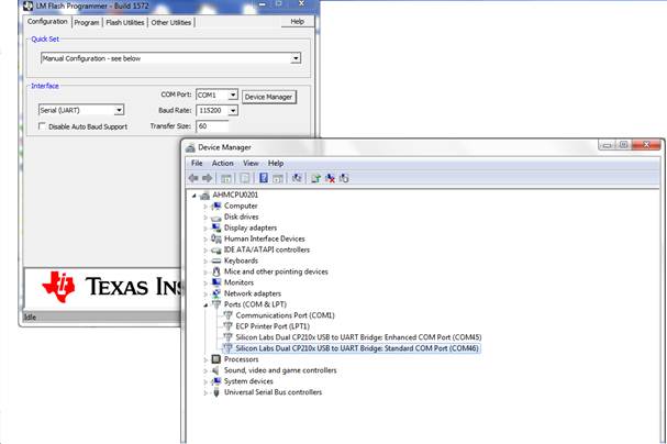
6.3.5.3.3. UCD Power Management Update
There is one power management module (a.k.a. UCD) located on the EVM. It can be identified by its address: 104(68h). Each module contains non-volatile registers that determine its operation. It may be necessary to update these registers in the field after the board has been shipped.
This update can be performed through the BMC, which can issue commands to the UCD modules to update the register settings. The Power Management Configuration Update Tool performs the task of sending commands to the BMC to get the current module versions, and perform updates using configuration files.
The latest version of the tool is available from here along with instructions on using the tool, and the latest configuration files (txt files). Please follow the instructions provided to check the current module versions, and update them accordingly.
Note
The DIP switch configuration of the board when running the update is irrelevant.
6.3.6. EVMK2H Hardware Setup Guide
6.3.6.1. Hardware Setup
Note
The EVM board is sensitive to electrostatic discharges (ESD). Use a grounding strap or other device to prevent damaging the board. Be sure to connect communication cables before applying power to any equipment.
6.3.6.1.1. FTDI Driver Installation on PC Host
The K2 EVM has a FTDI FT2332HL device on board. A driver must be installed on the PC Host in order to be able to communicate with the EVM using the FTDI mini-USB connector located under the mini-USB connector of the emulator daughter card. The driver can be downloaded from here FTDI Driver.
Note
Before testing the usb connection, make sure that the mini-usb cable is plugged into the port on the base board. (and not connected to the daughter card).
After installing the driver and connecting the USB cable, two COM ports should be visible in the list of COM ports available to connect to in the PC Host terminal console. The lower COM port corresponds to the SoC UART and the higher one corresponds to the MCU UART.
6.3.6.1.2. BMC Version Check and Update
Read BMC_In-Field_Update to check BMC version and update if necessary.
6.3.6.1.3. UCD Power Management Modules In-Field Update
There are three power management modules (sometimes called the UCDs)
located on the EVM. Each module can be identified by it’s address:
104(68h), 52(34h), and 78(4Eh). Each module contains non-volatile
registers that determine it’s operation. It may be necessary to update
these registers after the board has been shipped. This update can be
performed through the BMC, which can issue commands to the UCD modules
to update the register settings. The Power Management Configuration
Update Tool (bmc_tool.py) performs the task of sending commands to
the BMC to get the current module versions, and perform updates using
configuration files. Instructions for executing the update tool
(bmc_tool.py) are available here: BMC Tool UCD Update Guide
The latest version of the tool is available here. The latest configuration files (txt files) are available here. Please follow the instructions provided to check the current module versions, and update them accordingly.
Note
The DIP switch configuration of the board when running the update is irrelevant.
Note
BMC versions 1.0.1.3a and earlier will not work properly with the Get Versions feature of the Update Tool. Upgrade to a more recent version of the BMC to use this functionality.
6.3.6.1.4. Attach the Ethernet cable
Using the Ethernet cable supplied, connect one end of the cable to the Ethernet Port 0 (marked ENET0 on the board) on the EVM and the other end to your PC.
This picture shows which Ethernet Port is 0:
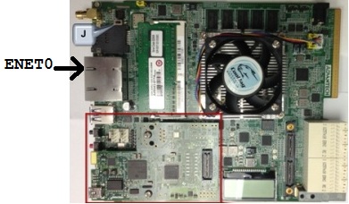
6.3.6.1.5. Connect the JTAG interface
Use the USB to USB mini-B cable provided. Connect the USB mini-B connector to the USB mini-B interface on the XDS-2xx daughter card on the EVM, and the USB connector to your PC. This enables XDS-2xx emulation and is directly useable by CCS. If you are using a different JTAG, connect it now.
6.3.6.1.6. K2H Set the boot mode switch SW1
K2H No Boot/JTAG DSP Little Endian Boot mode
For Rev 0B EVM, the setting is as follows
SW1 - 4(ON) 3(ON) 2(ON) 1(OFF)
For Rev 1.0 EVM, the setting is as follows:
SW1 - 1(OFF) 2(OFF) 3(OFF) 4(ON)
K2H SPI Little Endian Boot mode
For Rev 0B EVM, the setting is as follows:
SW1 - 4(ON) 3(ON) 2(OFF) 1(ON)
For Rev 1.0 EVM, the setting is as follows:
SW1 - 1(OFF) 2(OFF) 3(ON) 4(OFF)
6.3.6.1.7. DDR Configuration (Rev 0B EVM only)
For Rev 0B EVM, the following procedure is required for proper DDR configuration:
- Connect the MCU UART port to PC using the serial cable provided with the EVM. The MCU UART port is the 4-pin white connector farthest from the edge of the EVM. Alternatively it is also possible to connect a mini-USB cable to the FTDI mini-USB connector of the EVM. This will provide access to both the SoC and the MCU UART ports.
- Start Tera Term or Hyper terminal and set to 115200 board rate, 8-bit data, 1-bit stop and no parity/flow control.
- Power on the EVM. MCU UART console will show user prompt once MCU boot up is complete. Type the following commands at the console to setup DDR3A. Ethernet requires DDR3A and will not work with DDR3B which is default in Rev 0B EVMs.
BMC> setboot 100001
BMC> fullrst
6.3.6.1.8. Attach the serial port cable to the SoC UART port
Connect the SoC UART port to PC using the serial cable provided with the EVM. The SoC UART port is the 4-pin white connector closest to the edge of the EVM.
Start Tera Term or Hyper terminal and set to 115200 board rate, 8-bit data, 1-bit stop and no parity/flow control.
6.3.6.1.9. Connect the power cable
Connect the power cable to the EVM power jack on the board. To be ESD safe, plug in the other end of the power cable only after you have connected the power cord to the board. Then turn on the board.
6.3.6.2. BMC In-Field Update
BMC, or Board Management Controller, takes care of the power, clocks, resets, bootmodes, etc. of the EVM.
For Rev1.0 EVMs an in-field update may be necessary as a very small quantity were delivered with an old revision of the BMC. If your EVM is using version 1.0.1.3 then it should be updated to version 1.0.1.3a. The update corrects the way that the boot mode pins are interpreted.
You can check the version by:
1. Opening a hyperterminal or another similar type of console application.
2. Set COM Port to higher value
- When you connect to FTDI mini-USB on the EVM it will provide 2 COM port connections, one to the SOC UART and one to BMC UART.
- The SOC UART will always be the lowest value COM port, for example COM5, and the BMC UART will always be the higher value COM port, for example COM6. (Actual COM PORT values will vary).
3. Set COM port properties appopriately:
- Baud Rate or Bits per second: 115200
- Data Bits: 8
- Parity: None
- Stop Bits: 1
- Flow Control: None
4. At BMC prompt typer ‘ver’ (no quotes)
5. Check BMC Version
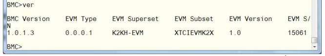
If an in-field update is needed, downloaded the latest version here (labeled Board Management Controller Binaries (BMC)) and continue with the following steps.
Prepare EVM for in-field update:
- Remove power to the EVM.
- Set boot mode to “No Boot mode” ( See NoBootLittleEndian_ )
- Remove the MCU_BOOTSELECT (CN9) jumper (see picture below for location of jumper: Referred as “G: MCU Reset Jumper for BMC field update”).
- Make sure your USB cable is connected to FTDI mini-USB (not XDS200 Emulator USB) OR connect 4pin UART cable to COM1: MCU UART connector.
- Make sure no HyperTerminal/Console connected to BMC COM port are open or active.
- Use the LM Flash Programmer (available here) to update the firmware, as detailed in the steps below.
Perform in-field update:
Apply power to the EVM. No LED’s will be illuminated and no LCD backlight or characters will be on because the BMC is waiting for a command rather than executing from Flash.
Open the LM Flash programmer utility. (Default location Start Menu -> All Programs -> Texas Instruments -> Stellaris -> LM Flash Programmer -> LM Flash Programmer )
In the LM Flash Programmer Utility ‘Configuration’ tab, in the interface section, select ‘Serial (UART)’ from the drop-down box on the left.
Select the BMC COM Port (the same COM port used to issue the ver command earlier), and set the ‘Baud Rate’ to 115200.
Set ‘Transfer Size’ to 60, and make sure ‘Disable Auto Baud Support’ is unchecked.
In the ‘Program’ tab, Browse to the location of the binary file containing the firmware update, and select it.
Leave all other options as default, and press the ‘Program’ button.
After the programming is complete, power off the board.
Reconnect the jumper.
Open the HyperTerminal/Console for the BMC COM port.
Apply power to the EVM. When BMC completes initialization of board it will show latest version of BMC in Console.
If step 9 was done after power was applied, just type “ver” at BMC prompt.
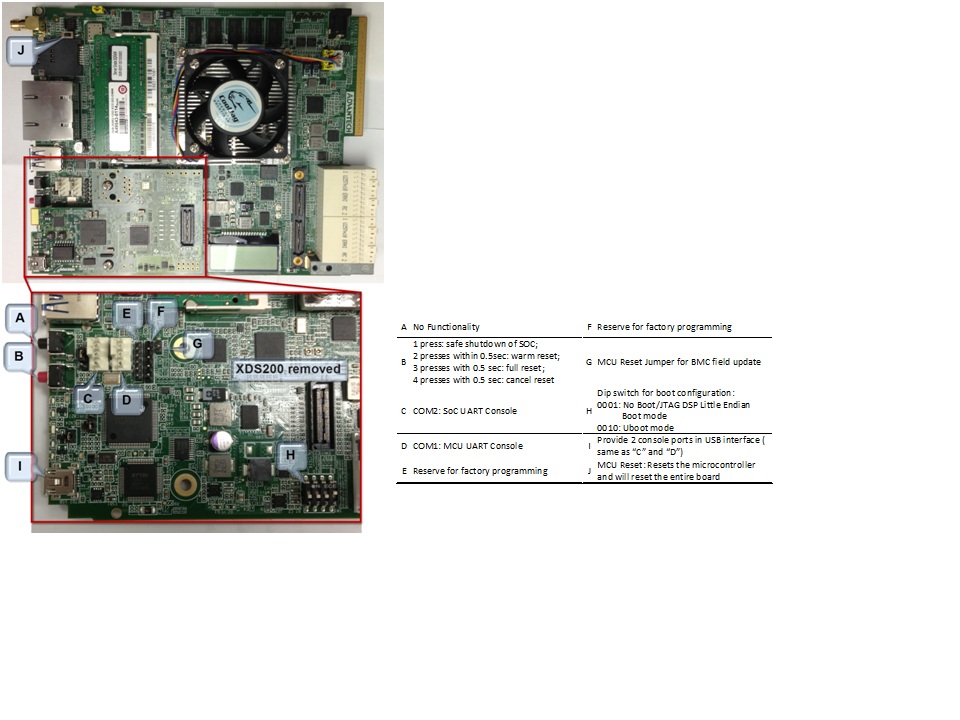
6.3.6.3. DIP Switch and Bootmode Configurations
6.3.6.3.1. Rev 1.0 EVM SW1 switch Bootmode Configuration
| DIP Switch (p1, p2, p3, p4) | Bootmode |
|---|---|
| 0000 | ARM NAND |
| 0001 | DSP no-boot |
| 0010 | ARM SPI |
| 0011 | ARM I2C |
| 0100 | ARM UART |
| 0101 | Reserved |
| 0110 | Reserved |
| 0111 | Reserved |
| 1000 | Reserved |
| 1001 | Reserved[1] |
| 1010 | Reserved |
| 1011 | Reserved |
| 1100 | Reserved |
| 1101 | Reserved |
| 1110 | Reserved |
| 1111 | Reserved |
[1]In revision BMC v1.0.1.4 this is 10 MHz SPI NOR. This will not continue in future versions.
6.3.6.3.2. Changing the Bootmode
In BMC v1.0.1.x the only way to use a bootmode that is not supported by the DIP switch combinations is to use the ‘setboot’ and ‘fullrst’ commands. To set the bootmode use the setboot command, which takes a 32 bit value in hex as its only argument:
setboot 00110CE7
Then use the fullrst command to boot the SoC into this bootmode:
fullrst
This process is volatile, and will have to be repeated every time the board is power cycled.
In BMC v1.0.2.x the setboot command has been removed. It has been replaced with the bootmode command, which performs various functions depending on the way in which the command is used. The command works with 16 bootmodes, which are representative of the various DIP switch combinations; the bootmodes are numbered 0 - 15. Bootmodes 8 - 15 are User-Defined, and may be altered and stored using the command (explained below). Each bootmode consists of a title, a high value, and a low value. The high value is currently not used. The low value is a 32 bit value in hex, and is the same as the value previously used by setboot. The bits of low value (and the setboot argument) are shown in the table below).
| Bit | Devstat Bit | Config Pin Function | Normal Pin Function | Comments |
|---|---|---|---|---|
| 31 | Reserved | |||
| 30 | Reserved | |||
| 29 | Reserved | |||
| 28 | Reserved | |||
| 27 | Reserved | |||
| 26 | Reserved | |||
| 25 | PACLKSEL | PACLKSEL | ||
| 24 | CORECLKSEL | CORECLKSEL | ||
| 23 | Reserved | |||
| 22 | AVSIFSEL1 | TIMI1 | Reserved: EVM forces these bits to strap values during reset | |
| 21 | AVSIFSEL0 | TIMI0 | Reserved: EVM forces these bits to strap values during reset | |
| 20 | DDR3_REMAP_EN | GPIO16 | ||
| 19 | ARM_LENDIAN | GPIO15 | 0 = little, 1 = is not supported; do in SW | |
| 18 | MAINPLLODSEL | CORESEL3 | ||
| 17 | ARMAVSSHARED | CORESEL2 | ||
| 16 | 16 | BOOTMODE15 | CORESEL2 | |
| 15 | 15 | BOOTMODE14 | CORESEL1 | Element |
| 14 | 14 | BOOTMODE13 | CORESEL0 | |
| 13 | 13 | BOOTMODE12 | GPIO13 | |
| 12 | 12 | BOOTMODE11 | GPIO12 | |
| 11 | 11 | BOOTMODE10 | GPIO11 | |
| 10 | 10 | BOOTMODE9 | GPIO10 | |
| 9 | 9 | BOOTMODE8 | GPIO9 | |
| 8 | 8 | BOOTMODE7 | GPIO8 | |
| 7 | 7 | BOOTMODE6 | GPIO7 | |
| 6 | 6 | BOOTMODE5 | GPIO6 | |
| 5 | 5 | BOOTMODE4 | GPIO5 | |
| 4 | 4 | BOOTMODE3 | GPIO4 | |
| 3 | 3 | BOOTMODE2 | GPIO3 | |
| 2 | 2 | BOOTMODE1 | GPIO2 | |
| 1 | 1 | BOOTMODE0 | GPIO1 | |
| 0 | 0 | LENDIAN | GPIO0 |
There are 5 different formats to the bootmode command:
bootmode
When the command is entered with no arguments the current bootmode will be displayed.
bootmode all
This format will display all 16 bootmodes and mark the currently selected bootmode.
bootmode #x
This will change the currently selected bootmode to the bootmode represented by x. For example, if the board is booted with DIP switch setting 1(OFF) 2(OFF) 3(OFF) 4(ON) then the bootmode would be 1 - DSP NO-BOOT. If ‘bootmode #2’ is entered, the bootmode represented by DIP switch setting 1(OFF) 2(OFF) 3(ON) 4(OFF) would become the current bootmode (ARM SPI-NOR BOOT). If the ‘reboot’ command is given, the SoC will be rebooted using this new bootmode. This format is volatile, meaning once power is removed, the bootmode at the next power up will be determined by the DIP switch.
bootmode read
This format reads the current value of the DIP switch, and changes the current bootmode to this value. For example, if the board is booted with DIP switch setting 1(OFF) 2(OFF) 3(OFF) 4(ON) then the bootmode would be 1 - DSP NO-BOOT. If the DIP switch is changed to 1(OFF) 2(OFF) 3(ON) 4(OFF) and then the command ‘bootmode read’ is given, the board will change to bootmode 2 - ARM SPI-NOR BOOT. If the ‘reboot command is then given, the SoC will be rebooted using this new bootmode.
bootmode [#]x hi_value lo_value title
This bootmode is used to alter User-Defined bootmodes (bootmodes 8 - 15). x is the index of the bootmode to be set, as such its appropriate value range is 8 - 15, any other value will return an error. hi_value is not currently used, and should always be set to 0. lo_value is a 32 bit hex value whose bits are representative of the table above. title is a given string that is displayed by the bootmode command to help better understand what the bootmode does, it has no purpose within the actual booting of the board. The option ‘#’ is used to determine whether the bootmode will be saved. If # is used, the bootmode will be saved to flash, meaning the new value is tied to the DIP switch, and will remain even if power is removed from the board. If # is not given, then the change will be lost as soon as power is removed. Some examples with descriptions are given below:
bootmode 8 0 112005 ARM_SPI
bootmode 8 will be set to 112005 and given the title ARM_SPI. To boot into this bootmode, the command ‘bootmode #8’ followed by ‘reboot’ would be given (or changing the DIP switch to 1(ON) 2(OFF) 3(OFF) 4(OFF) without removing power, then entering ‘bootmode read’ followed by ‘reboot’). Once power is removed, this change is lost.
bootmode #10 0 12cba1 RANDOM_BOOT
bootmode 10 will be set to 12cba1 and given the title RANDOM_BOOT. This is now the permanent value of bootmode 10; the change will persist even if power is removed.
6.3.6.4. Connect to EVMK2H using CCS
Step 1: Configure the EVM hardware
- Setup the EVM to DSP no boot using SW1 as described in the section BootModeConfiguration
- Connect mini USB cable to the XDS2xx MIPI adapter card marked J1 or connect external emulator to the MIPI connector on J3
Note
For newer versions of CCS, a XDS200 firmware update is recommended which user can perform using instruction on the article
below:
Note
For newer versions of CCS, a XDS200 firmware update is recommended which user can perform using instruction on
Updating_the_XDS200_firmware <https://dev.ti.com/tirex/explore/node?node=AADzJ8Y-La4f7Bi5Ga0TcA__FUz-xrs__LATEST>__
Step 2: Create CCS Target configuration
Launch CCS on your host machine. Select View Tab and select the “Target configuration”
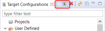
Create New Target configuration in CCS by selecting appropriate emulator. For Default on board emulator select “Texas instruments XDS2xx Debug Probe” and select the target device as 66AK2H12.
Go to the Advanced Tab where you will see all the cores on the SOC listed. In order to initialize the clocks and external DDR memory on the device, users are required to use a initialization Gel scripts. To populate the Gel Select A15_0 and then hit Browse and locate the GEL in the CCS installation under the following path: CCS_INSTALL/ccs_base/emulation/boards/xtcievmk2x/gel
DSP developers, can also select C66x_0 and populate the DSP GEL file that is found in the same location.
Going back to the Basic Tab, Save the configuration. For additional sanity check, you can also test connection.
Step 3: Connect to the cores
Right click on the target configuration and Select “Launch Target configuration”. Wait for CCS debug View to launch and display the eight C66x cores and 4 A15 cores.
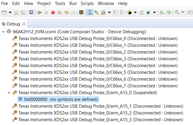
Start by connecting to A15_0 and C66x_0. when you connect to the cores, you will see the GEL script logs in the console window, which indicates that device clocks, PSC and external DDR memory has been initialized. The GEL log from target connect is provided below for reference.
arm_A15_0: GEL Output: Disabling MMU
arm_A15_0: GEL Output: Disabling Caches
arm_A15_0: GEL Output: Invalidate Instruction Caches
arm_A15_0: GEL Output: Enabling non-secure access to cp10 and cp11
arm_A15_0: GEL Output: Enabled non-secure access to cp10 and cp11
arm_A15_0: GEL Output: Enabling SMP bit in ACTLR
arm_A15_0: GEL Output: Enabled SMP bit in ACTLR
arm_A15_0: GEL Output: Entering NonSecure Mode
arm_A15_0: GEL Output: Entered NonSecure Mode
arm_A15_0: GEL Output: Disabling MMU
arm_A15_0: GEL Output: Disabling Caches
arm_A15_0: GEL Output: Invalidate Instruction Caches
arm_A15_0: GEL Output:
Connecting Target...
arm_A15_0: GEL Output: Disabling MMU
arm_A15_0: GEL Output: Disabling Caches
arm_A15_0: GEL Output: Invalidate Instruction Caches
arm_A15_0: GEL Output: Enabling non-secure access to cp10 and cp11
arm_A15_0: GEL Output: Enabled non-secure access to cp10 and cp11
arm_A15_0: GEL Output: Enabling SMP bit in ACTLR
arm_A15_0: GEL Output: Enabled SMP bit in ACTLR
arm_A15_0: GEL Output: Entering NonSecure Mode
arm_A15_0: GEL Output: Entered NonSecure Mode
arm_A15_0: GEL Output: Disabling MMU
arm_A15_0: GEL Output: Disabling Caches
arm_A15_0: GEL Output: Invalidate Instruction Caches
arm_A15_0: GEL Output: TCI6638K2K GEL file Ver is 1.89999998
arm_A15_0: GEL Output: Disabling MMU
arm_A15_0: GEL Output: Disabling Caches
arm_A15_0: GEL Output: Invalidate Instruction Caches
arm_A15_0: GEL Output: Enabling non-secure access to cp10 and cp11
arm_A15_0: GEL Output: Enabled non-secure access to cp10 and cp11
arm_A15_0: GEL Output: Enabling SMP bit in ACTLR
arm_A15_0: GEL Output: Enabled SMP bit in ACTLR
arm_A15_0: GEL Output: Entering NonSecure Mode
arm_A15_0: GEL Output: Entered NonSecure Mode
arm_A15_0: GEL Output: Disabling MMU
arm_A15_0: GEL Output: Disabling Caches
arm_A15_0: GEL Output: Invalidate Instruction Caches
arm_A15_0: GEL Output: Detected PLL bypass disabled: SECCTL[BYPASS] = 0x00000000
arm_A15_0: GEL Output: (3a) PLLCTL = 0x00000040
arm_A15_0: GEL Output: (3b) PLLCTL = 0x00000040
arm_A15_0: GEL Output: (3c) Delay...
arm_A15_0: GEL Output: (4)PLLM[PLLM] = 0x0000000F
arm_A15_0: GEL Output: MAINPLLCTL0 = 0x07000000
arm_A15_0: GEL Output: (5) MAINPLLCTL0 = 0x07000000
arm_A15_0: GEL Output: (5) MAINPLLCTL1 = 0x00000040
arm_A15_0: GEL Output: (6) MAINPLLCTL0 = 0x07000000
arm_A15_0: GEL Output: (7) SECCTL = 0x00090000
arm_A15_0: GEL Output: (8a) Delay...
arm_A15_0: GEL Output: PLL1_DIV3 = 0x00008002
arm_A15_0: GEL Output: PLL1_DIV4 = 0x00008004
arm_A15_0: GEL Output: PLL1_DIV7 = 0x00000000
arm_A15_0: GEL Output: (8d/e) Delay...
arm_A15_0: GEL Output: (10) Delay...
arm_A15_0: GEL Output: (12) Delay...
arm_A15_0: GEL Output: (13) SECCTL = 0x00090000
arm_A15_0: GEL Output: (Delay...
arm_A15_0: GEL Output: (Delay...
arm_A15_0: GEL Output: (14) PLLCTL = 0x00000041
arm_A15_0: GEL Output: PLL has been configured (CLKIN * PLLM / PLLD / PLLOD = PLLOUT):
arm_A15_0: GEL Output: PLL has been configured (122.879997 MHz * 16 / 1 / 2 = 983.039978 MHz)
arm_A15_0: GEL Output: Switching on ARM Core 0
arm_A15_0: GEL Output: Switching on ARM Core 1
arm_A15_0: GEL Output: Switching on ARM Core 2
arm_A15_0: GEL Output: Switching on ARM Core 3
arm_A15_0: GEL Output: ARM PLL has been configured (125.0 MHz * 16 / 2 = 1000.0 MHz)
arm_A15_0: GEL Output:  DISABLESTAT ---> 0x00000000
arm_A15_0: GEL Output: Power on all PSC modules and DSP domains...
arm_A15_0: GEL Output: Power on all PSC modules and DSP domains... Done.
arm_A15_0: GEL Output: WARNING: SYSCLK is the input to the PA PLL.
arm_A15_0: GEL Output: Completed PA PLL Setup
arm_A15_0: GEL Output: PAPLLCTL0 - before: 0x0x09080500  after: 0x0x09080500
arm_A15_0: GEL Output: PAPLLCTL1 - before: 0x0x00002040  after: 0x0x00002040
arm_A15_0: GEL Output: DDR begin
arm_A15_0: GEL Output: XMC setup complete.
arm_A15_0: GEL Output: DDR3 PLL (PLL2) Setup ...
arm_A15_0: GEL Output: DDR3 PLL Setup complete, DDR3A clock now running at 666 MHz.
arm_A15_0: GEL Output: DDR3A initialization complete
arm_A15_0: GEL Output: DDR3 PLL Setup ...
arm_A15_0: GEL Output: DDR3 PLL Setup complete, DDR3B clock now running at 800MHz.
arm_A15_0: GEL Output: DDR3B initialization complete
arm_A15_0: GEL Output: DDR done
arm_A15_0: GEL Output: Entering A15 non secure mode ..
arm_A15_0: GEL Output: Disabling MMU
arm_A15_0: GEL Output: Disabling Caches
arm_A15_0: GEL Output: Invalidate Instruction Caches
arm_A15_0: GEL Output: Enabling non-secure access to cp10 and cp11
arm_A15_0: GEL Output: Enabled non-secure access to cp10 and cp11
arm_A15_0: GEL Output: Enabling SMP bit in ACTLR
arm_A15_0: GEL Output: Enabled SMP bit in ACTLR
arm_A15_0: GEL Output: Entering NonSecure Mode
arm_A15_0: GEL Output: Entered NonSecure Mode
arm_A15_0: GEL Output: Disabling MMU
arm_A15_0: GEL Output: Disabling Caches
arm_A15_0: GEL Output: Invalidate Instruction Caches
arm_A15_0: GEL Output: A15 non secure mode entered
Users can now load and run code on the cores by using Run -> Load Program. Happy Debugging !!