5.2.1. AM65x EVM
5.2.1.1. EVM Layout and Key Components
Refer to the image below which highlights the key components available on the AM65x EVM.
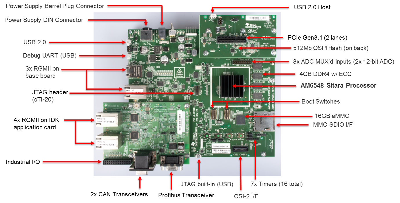
The complete feature set for the AM65x EVM is described in AM65x EVM User Manual. This section only provides description of components that are required to complete basic EVM setup for debugging code using an emulator and Code Composer Studio.
5.2.1.1.1. Supported JTAG Debug Probes (Emulators)
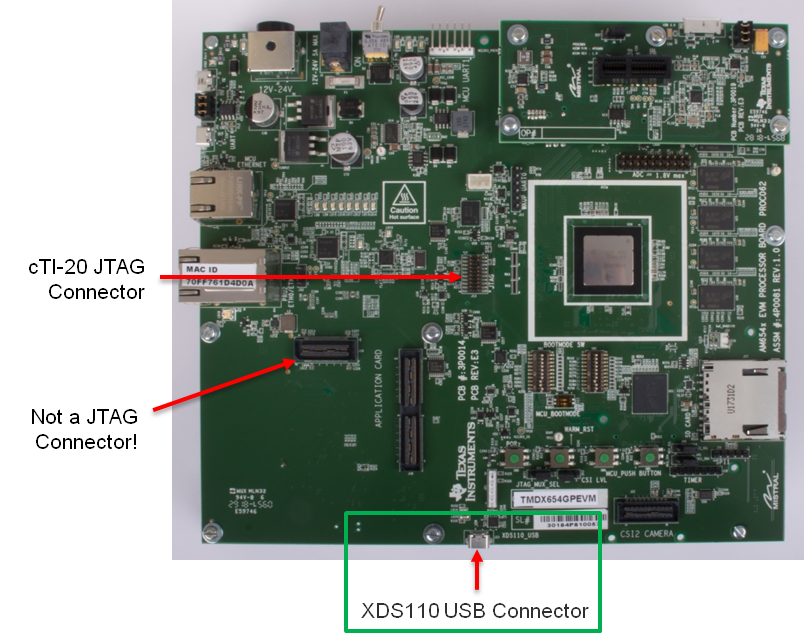
The AM65x EVM includes a cTI20 JTAG connector for external emulators and a micro USB connector for the on-board XDS110 emulator.
For XDS110 connect a USB cable to the micro USB connector J23 on the front of the board.
For external XDS200, connect the emulator to the cTI20 pin connector.
For Lauterbach or emulators with MIPI60 or TI14 pin connector, an adapter must be used to connect the emulator.
Warning
Do not connect an XDS560 emulator to the J16 application board connector. This may damage the EVM and the emulator pod.
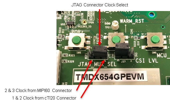
If you are using an external emulator pod, you must select which connector sources the clock. The AM65x EVM can support the MIPI60 or cTI20 connector. The JTAG select jumper must be set correctly to specify the clock source as either the MIPI60 or the cTI20 connector.
5.2.1.1.2. BOOTMODE Switches
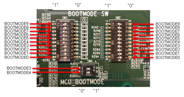
MCU BOOTMODE shown:
MCUBOOTMODE[8:0] – 0000 10 011
Values in bold are fixed with resistors.
BOOTMODE shown:
BOOTMODE[18:0] - 1111111000011110000
5.2.1.1.2.1. Recommended Boot Mode
BOOTMODE[18:0] = 000000000 0000000000 MCUBOOTMODE[8:0]= 000000011 (SLEEP BOOT)
- Boot Settings
- SW2 – All switches OFF
- SW3 – All switches OFF
BOOTMODE[18:0] = 000000100 0000000110 MCUBOOTMODE[8:0]= 000000011 (SD BOOT)
For full details on supported boot modes, please refer to the table below.
| SW3.4 | SW3.3 | SW3.2 | SW3.1 | Primary Boot Device Selected |
|---|---|---|---|---|
| OFF | OFF | OFF | OFF | Sleep (No boot - debug mode) |
| OFF | OFF | OFF | ON | OSPI |
| OFF | OFF | ON | OFF | QSPI |
| OFF | OFF | ON | ON | Hyperflash |
| OFF | ON | OFF | OFF | SPI (on QSPI/OSPI port 0 in legacy SPI mode) |
| OFF | ON | OFF | ON | I2C |
| OFF | ON | ON | OFF | MMC/SD card, eMMC boot from UDA or file system |
| OFF | ON | ON | ON | Ethernet |
| ON | OFF | OFF | OFF | USB |
| ON | OFF | OFF | ON | PCIe |
| ON | OFF | ON | OFF | UART |
| ON | OFF | ON | ON | Reserved |
| ON | ON | OFF | OFF | GPMC XIP |
| ON | ON | OFF | ON | eMMC boot from boot partition (with auto-fall back to file system) |
| ON | ON | ON | OFF | Reserved (acts as no boot) |
| ON | ON | ON | ON | Reserved (acts as no boot) |
Note
On the AM65x EVM, ensure that the PLL configuration is set to 25 MHz (see bolded line in table below).
| Bit 2 | Bit 1 | Bit 0 | PLL REF CLK (MHz) |
|---|---|---|---|
| 0 | 0 | 0 | Sleep (No boot - debug mode) |
| 0 | 0 | 1 | 20 |
| 0 | 1 | 0 | 24 |
| 0 | 1 | 1 | 25 |
| 1 | 0 | 0 | 26 |
| 1 | 0 | 1 | 27 |
| 1 | 1 | 0 | Reserved |
| 1 | 1 | 1 | No PLL Configuration Done (slow speed backup) |
5.2.1.1.3. UART Connection
- Connect a micro USB cable between UART port (J42) of the EVM and host PC.
- Open a serial console (e.g. Tera Term) on host PC, connect to COM port on which SOC UART0 port is connected. Four COM ports should appear in the serial console application. Connect to the first COM port in the list.
- First COM port – SoC MAIN UART0
- Second COM port – MCU UART
- Third COM port – Wakeup UART
- Fourth COM port – SoC MAIN UART1
- Open a serial console (e.g Tera Term) on host PC, connect to COM port on which EVM UART port is connected and set the following configuration.
- Baud rate - 115200
- Data length - 8 bit
- Parity - None
- Stop bits - 1
- Flow control - None
5.2.1.1.4. Powering the EVM
| Connector | Specifications | Example |
|---|---|---|
| Power DIN, 4-pin | 24VDC, 5A Output (Max) | CUI Inc.SDI120-24-U-P51 |
| Barrel Plug, 2.5mm I.D x 5.5mm O.D x 9.55 | 12-24VDC, positive center, 2.71A Output (Max) | CUI Inc. SDI65-24UD-P6 |
Note
The DIN connector power supply is recommended to provide enough power for applications that make use of the PCIe interface.
5.2.1.2. Minimum Hardware Setup Required to Connect to EVM
- Connect micro USB cable to J23 and connect USB to Host PC on which CCS is installed.
- Connect micro USB cable to J42 for UART serial IO.
- Set boot switches to “Sleep Boot” or “SD Boot” as described in the BOOT Switches section.
- Connect power supply to DC jack and power on EVM.
- Set switches and jumpers as indicated below.
- Boot Settings
- SW2 - All switches OFF
- SW3 - All switches OFF
- Jumpers
- J4 – Short all the pins
- JP37 – Short pins 1 & 2
- J43 - Short pins 1 & 2
- J8 – Short pins 1 & 2
5.2.1.3. AM65x Debug Software Setup
The following software packages are required to setup the AM65x EVM
- Code Composer Studio IDE Environment
- Processor SDK RTOS for AM65xx
5.2.1.3.1. CCS Host Setup
1. Download CCS from the following link: https://processors.wiki.ti.com/index.php/Download_CCS
Note
Check the Processor SDK Release Notes for the recommended CCS version.
Ensure that at least “Sitara AMx Processors” is selected:
5.2.1.3.1.1. Install the latest Emulation Package and Device Support Package
1. In CCS, navigate to Help -> Check for Updates and select “Sitara device support” and “TI Emulators” and click Next.
2. Click “Next” again, select “I accept the terms of the license agreements” and click Finish to begin the installation.
3. You may be prompted to restart CCS for the updates to take effect. Click “Restart Now” when prompted to complete the installation.
Disable Automatic Updates
To disable automatic updates in CCS, navigate to Windows -> Preferences -> Install/Update -> Automatic Updates, and uncheck “Automatically find new updates and notify me.”
This is a precautionary step to avoid automatic updates overwriting files updated through TI Emulation Updates for AM65x
5.2.1.3.2. Basic CCS Setup
The Basic CCS setup is similar to earlier Sitara devices which involves creation of target configuration and connecting to cores using the GEL files. This step is suitable for new board bring up and getting hello world going on the AM65x cores.
Users can use this setup for benchmarking code on cores, test basic pin functionality or to run diagnostics. However, multi-core application developers requiring resource management, power management or security services will require the advanced CCS setup in addition to the basic core setup.
We recommend that you follow the steps in basic setup and then migrate to the advanced SOC CCS setup for application development.
5.2.1.3.2.1. Creating the Target Configuration
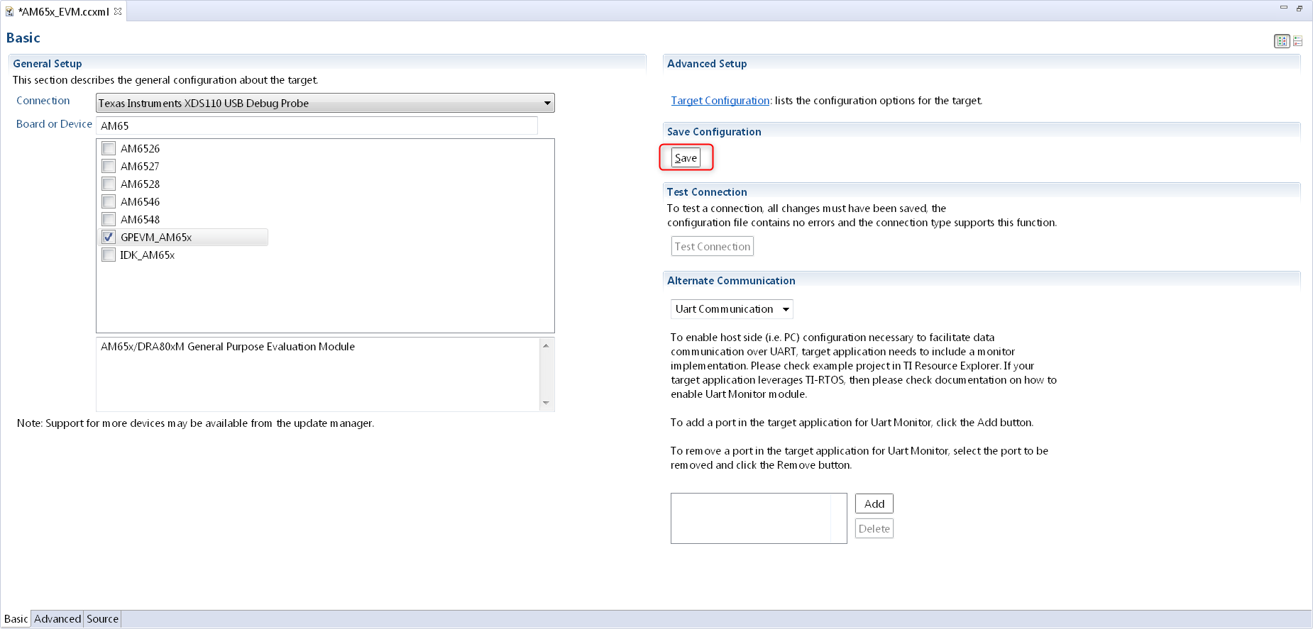
- In CCS, open the Target Configurations window by navigating to View -> Target Configurations.
- In Target Configurations, right click and select “New Target Configuration.”
- Populate the Target Configuration File name, set the location, and click Finish.
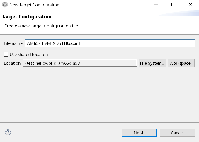
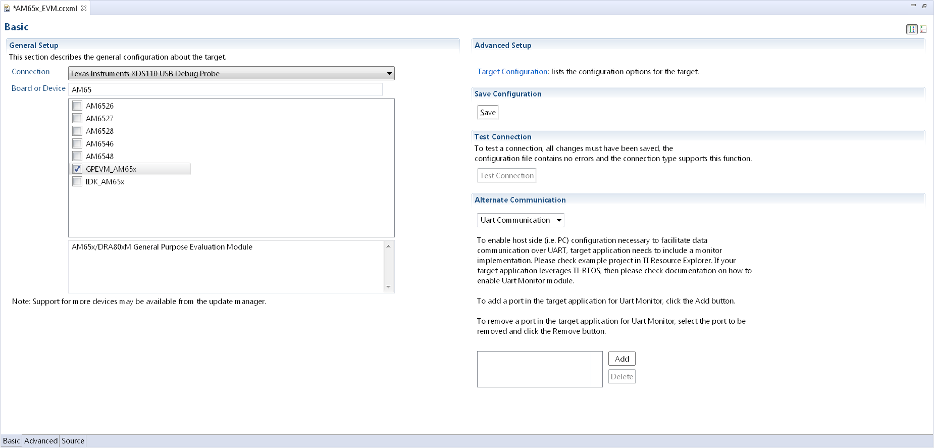
- Select “Texas Instruments XDS110 USB Debug Probe” for the Connection and “GPEVM_AM65x” for the Board or Device.
Note
The GEL files are automatically populated in the Target Configuration when selecting an EVM instead of an SOC. The SOC option is generally used for custom board bring up or secondary boot debugging.
- Navigate to the “Advanced” tab to ensure the GEL files are populated in the “initialization script” field for the various cores.
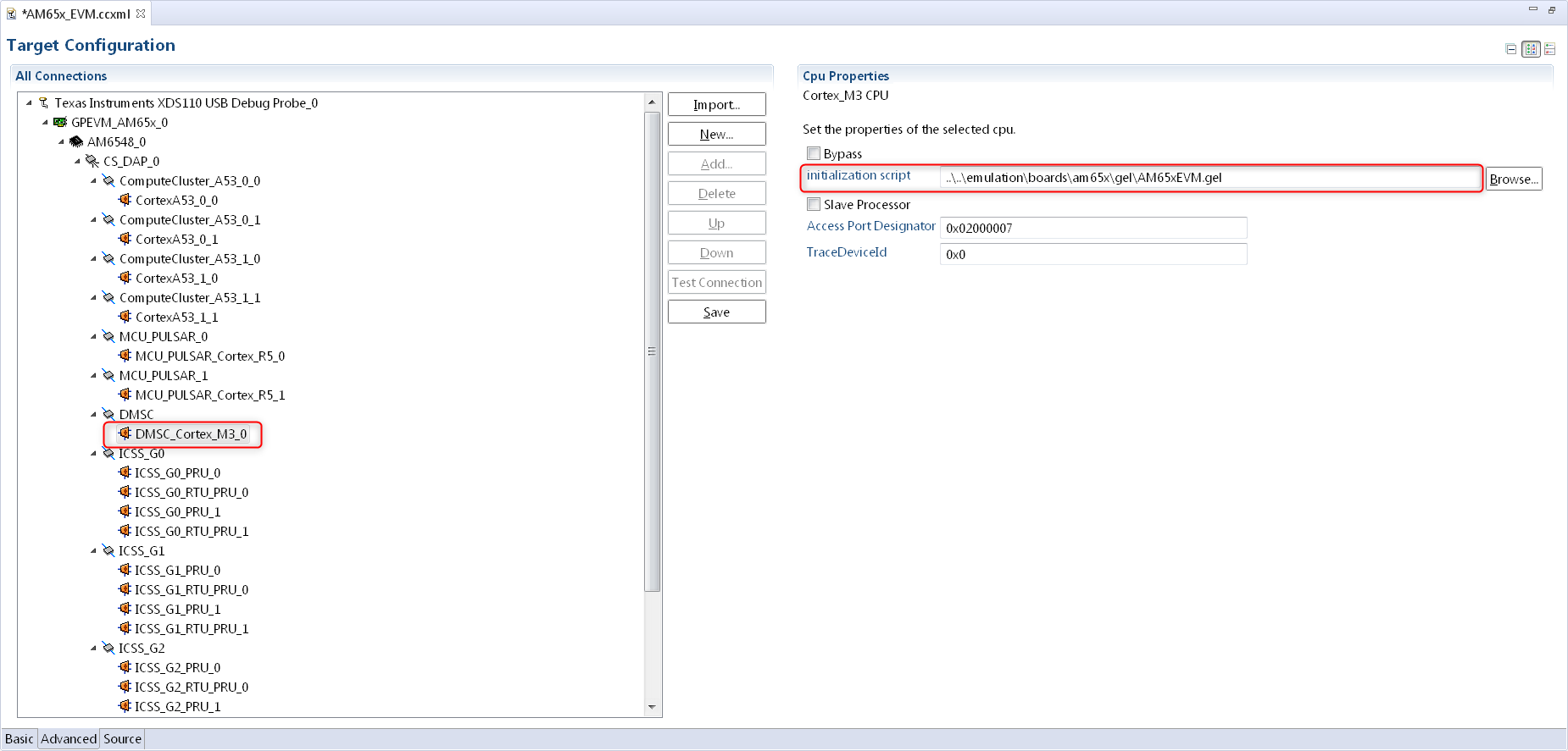
The initialization script for the Cortex M3 will setup the MCU domain and Main domain PLL clocks, PSC registers, and bring the R5 and Cortex A53 cores out of reset.
The initialization script for the Cortex A53 and Cortex R5 will perform a similar step to setup the DDR clocks and initialize DDR from the cores if required.
- Save the Target Configuration.
5.2.1.3.2.2. Connecting to the Cores on AM65x
1. Launch Target Configuration In CCS Editor View, go to View -> Target Configuration, and right click on the configuration that was created in the previous section and select “Launch Selected Configuration.”
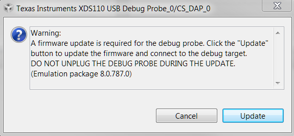
- Connect to DMSC_Cortex_M3
Note
When connecting to the M3 core for the first time, you may be prompted with a firmware update. Please click “Update” to update the emulator firmware.
On AM65x DMSC_Cortex_M3 is the boot master and is the first core that wakes up and starts the R5F ROM. Upon launching the target configuration, connect to DMSC_Cortex_M3 first, as this will automatically perform the PSC and PLL initialization. The following GEL output will appear in the CCS Console:
DMSC_Cortex_M3_0: GEL Output: Configuring AM65xEVM...
DMSC_Cortex_M3_0: GEL Output: Init value actual value: 0x00000888
DMSC_Cortex_M3_0: GEL Output: Register value: 0x00000888
DMSC_Cortex_M3_0: GEL Output: ATCM is on
DMSC_Cortex_M3_0: GEL Output: ATCM configured.
DMSC_Cortex_M3_0: GEL Output: Assuming execution from M3
DMSC_Cortex_M3_0: GEL Output: This script sets the first address translation region to [0x8000_0000, 0x0000_0000].
DMSC_Cortex_M3_0: GEL Output: It also sets the second address translation region to    [0x6000_0000, 0x4000_0000].
DMSC_Cortex_M3_0: GEL Output: Setting all PLLs in progress. This may take some time.
DMSC_Cortex_M3_0: GEL Output: 0 Percent Complete...
DMSC_Cortex_M3_0: GEL Output: 10 Percent Complete...
DMSC_Cortex_M3_0: GEL Output: 20 Percent Complete...
DMSC_Cortex_M3_0: GEL Output: 30 Percent Complete...
DMSC_Cortex_M3_0: GEL Output: 40 Percent Complete...
DMSC_Cortex_M3_0: GEL Output: 50 Percent Complete...
DMSC_Cortex_M3_0: GEL Output: 60 Percent Complete...
DMSC_Cortex_M3_0: GEL Output: 70 Percent Complete...
DMSC_Cortex_M3_0: GEL Output: 80 Percent Complete...
DMSC_Cortex_M3_0: GEL Output: 90 Percent Complete...
DMSC_Cortex_M3_0: GEL Output: Setting all PLLs done!
DMSC_Cortex_M3_0: GEL Output: Powering up all PSC power domains in progress...
DMSC_Cortex_M3_0: GEL Output: Powering up LPSC_WKUP_COMMON
DMSC_Cortex_M3_0: GEL Output: No change needed.
DMSC_Cortex_M3_0: GEL Output: Powering up LPSC_DMSC
DMSC_Cortex_M3_0: GEL Output: No change needed.
DMSC_Cortex_M3_0: GEL Output: Powering up LPSC_WKUP2MCU
DMSC_Cortex_M3_0: GEL Output: No change needed.
DMSC_Cortex_M3_0: GEL Output: Powering up LPSC_WKUP2MAIN_INFRA
DMSC_Cortex_M3_0: GEL Output: No change needed.
DMSC_Cortex_M3_0: GEL Output: Powering up LPSC_DEBUG2DMSC
DMSC_Cortex_M3_0: GEL Output: No change needed.
DMSC_Cortex_M3_0: GEL Output: Powering up LPSC_WKUP_GPIO
DMSC_Cortex_M3_0: GEL Output: No change needed.
DMSC_Cortex_M3_0: GEL Output: Powering up LPSC_MCU2MAIN_INFRA
DMSC_Cortex_M3_0: GEL Output: No change needed.
DMSC_Cortex_M3_0: GEL Output: Powering up LPSC_MCU2MAIN
DMSC_Cortex_M3_0: GEL Output: No change needed.
DMSC_Cortex_M3_0: GEL Output: Powering up LPSC_MCU2WKUP
DMSC_Cortex_M3_0: GEL Output: No change needed.
DMSC_Cortex_M3_0: GEL Output: Powering up LPSC_MAIN2MCU
DMSC_Cortex_M3_0: GEL Output: No change needed.
DMSC_Cortex_M3_0: GEL Output: Powering up LPSC_MCU_COMMON
DMSC_Cortex_M3_0: GEL Output: No change needed.
DMSC_Cortex_M3_0: GEL Output: Powering up LPSC_MCU_TEST
DMSC_Cortex_M3_0: GEL Output: No change needed.
DMSC_Cortex_M3_0: GEL Output: Powering up LPSC_MCU_MCAN_0
DMSC_Cortex_M3_0: GEL Output: No change needed.
DMSC_Cortex_M3_0: GEL Output: Powering up LPSC_MCU_MCAN_1
DMSC_Cortex_M3_0: GEL Output: No change needed.
DMSC_Cortex_M3_0: GEL Output: Powering up LPSC_MCU_OSPI_0
DMSC_Cortex_M3_0: GEL Output: No change needed.
DMSC_Cortex_M3_0: GEL Output: Powering up LPSC_MCU_OSPI_1
DMSC_Cortex_M3_0: GEL Output: No change needed.
DMSC_Cortex_M3_0: GEL Output: Powering up LPSC_MCU_HYPERBUS
DMSC_Cortex_M3_0: GEL Output: No change needed.
DMSC_Cortex_M3_0: GEL Output: Powering up LPSC_MCU_DEBUG
DMSC_Cortex_M3_0: GEL Output: No change needed.
DMSC_Cortex_M3_0: GEL Output: Powering up LPSC_MCU_R5_0
DMSC_Cortex_M3_0: GEL Output: No change needed.
DMSC_Cortex_M3_0: GEL Output: Powering up LPSC_MCU_R5_1
DMSC_Cortex_M3_0: GEL Output: No change needed.
DMSC_Cortex_M3_0: GEL Output: Powering up LPSC_MAIN_INFRA
DMSC_Cortex_M3_0: GEL Output: No change needed.
DMSC_Cortex_M3_0: GEL Output: Powering up LPSC_MAIN_TEST
DMSC_Cortex_M3_0: GEL Output: No change needed.
DMSC_Cortex_M3_0: GEL Output: Powering up LPSC_MAIN_PBIST
DMSC_Cortex_M3_0: GEL Output: No change needed.
DMSC_Cortex_M3_0: GEL Output: Powering up LPSC_CC_TOP
DMSC_Cortex_M3_0: GEL Output: No change needed.
DMSC_Cortex_M3_0: GEL Output: Powering up LPSC_A53_CLUSTER_0
DMSC_Cortex_M3_0: GEL Output: Power domain and module state changed successfully.
DMSC_Cortex_M3_0: GEL Output: Powering up LPSC_A53_0
DMSC_Cortex_M3_0: GEL Output: Power domain and module  state changed successfully.
DMSC_Cortex_M3_0: GEL Output: Powering up LPSC_A53_1
DMSC_Cortex_M3_0: GEL Output: Power domain and module state changed successfully.
DMSC_Cortex_M3_0: GEL Output: Powering up LPSC_A53_CLUSTER_1
DMSC_Cortex_M3_0: GEL Output: Power domain and module state changed successfully.
DMSC_Cortex_M3_0: GEL Output: Powering up LPSC_A53_2
DMSC_Cortex_M3_0: GEL Output: Power domain and module state changed successfully.
DMSC_Cortex_M3_0: GEL Output: Powering up LPSC_A53_3
DMSC_Cortex_M3_0: GEL Output: Power domain and module state changed successfully.
DMSC_Cortex_M3_0: GEL Output: Powering up LPSC_MAIN_DEBUG
DMSC_Cortex_M3_0: GEL Output: No change needed.
DMSC_Cortex_M3_0: GEL Output: Powering up LPSC_DSS
DMSC_Cortex_M3_0: GEL Output: Power domain and module state changed successfully.
DMSC_Cortex_M3_0: GEL Output: Powering up LPSC_MMC
DMSC_Cortex_M3_0: GEL Output: No change needed.
DMSC_Cortex_M3_0: GEL Output: Powering up LPSC_CAL
DMSC_Cortex_M3_0: GEL Output: Power domain and module state changed successfully.
DMSC_Cortex_M3_0: GEL Output: Powering up LPSC_PCIE_0
DMSC_Cortex_M3_0: GEL Output: Power domain and module state changed successfully.
DMSC_Cortex_M3_0: GEL Output: Powering up LPSC_PCIE_1
DMSC_Cortex_M3_0: GEL Output: Power domain and module state changed successfully.
DMSC_Cortex_M3_0: GEL Output: Powering up LPSC_USB_0
DMSC_Cortex_M3_0: GEL Output: Power domain and module state changed successfully.
DMSC_Cortex_M3_0: GEL Output: Powering up LPSC_USB_1
DMSC_Cortex_M3_0: GEL Output: Power domain and module state changed successfully.
DMSC_Cortex_M3_0: GEL Output: Powering up LPSC_SAUL
DMSC_Cortex_M3_0: GEL Output: No change needed.
DMSC_Cortex_M3_0: GEL Output: Powering up LPSC_PER_COMMON
DMSC_Cortex_M3_0: GEL Output: No change needed.
DMSC_Cortex_M3_0: GEL Output: Powering up LPSC_NB
DMSC_Cortex_M3_0: GEL Output: No change needed.
DMSC_Cortex_M3_0: GEL Output: Powering up LPSC_SERDES_0
DMSC_Cortex_M3_0: GEL Output: Power domain and module state changed successfully.
DMSC_Cortex_M3_0: GEL Output: Powering up LPSC_SERDES_1
DMSC_Cortex_M3_0: GEL Output: Power domain and module state changed successfully.
DMSC_Cortex_M3_0: GEL Output: Powering up LPSC_ICSSG_0
DMSC_Cortex_M3_0: GEL Output: Power domain and module state changed successfully.
DMSC_Cortex_M3_0: GEL Output: Powering up LPSC_ICSSG_1
DMSC_Cortex_M3_0: GEL Output: Power domain and module state changed successfully.
DMSC_Cortex_M3_0: GEL Output: Powering up LPSC_ICSSG_2
DMSC_Cortex_M3_0: GEL Output: Power domain and module state changed successfully.
DMSC_Cortex_M3_0: GEL Output: Powering up LPSC_GPU
DMSC_Cortex_M3_0: GEL Output: Power domain and module state changed successfully.
DMSC_Cortex_M3_0: GEL Output: Powering up LPSC_EMIF_DATA
DMSC_Cortex_M3_0: GEL Output: Power domain and module state changed successfully.
DMSC_Cortex_M3_0: GEL Output: Powering up LPSC_EMIF_CFG
DMSC_Cortex_M3_0: GEL Output: Power domain and module state changed successfully.
DMSC_Cortex_M3_0: GEL Output: Powering up all PSC power domains done!
3. Connect to Cortex A53 or Cortex R5F Users must now connect to either the Cortex A53 (CortexA53_0_0) or Cortex R5 (MCU_PULSAR_Cortex_R5_0). The following GEL output will appear in the CCS console when connecting to the Cortex A53:
CortexA53_0_0: GEL Output: VTT Regulator Enabled
CortexA53_0_0: GEL Output:
PHY Init complete
CortexA53_0_0: GEL Output: DDRSS_DDRPHY_PGSR0 = 0x8000000F
CortexA53_0_0: GEL Output:
Waiting for DRAM Init to complete...
CortexA53_0_0: GEL Output:
DRAM Init complete
CortexA53_0_0: GEL Output: DDRSS_DDRPHY_PGSR0 = 0x8000001F
CortexA53_0_0: GEL Output:
Waiting for write leveling to complete
CortexA53_0_0: GEL Output:
Write leveling complete
CortexA53_0_0: GEL Output: DDRSS_DDRPHY_PGSR0 = 0x8000003F
CortexA53_0_0: GEL Output: checking status per byte...
CortexA53_0_0: GEL Output:
DDRSS_DDRPHY_DX0GSR0 = 0x00932420
CortexA53_0_0: GEL Output:
DDRSS_DDRPHY_DX1GSR0 = 0x009224A0
CortexA53_0_0: GEL Output:
DDRSS_DDRPHY_DX2GSR0 = 0x00992620
CortexA53_0_0: GEL Output:
DDRSS_DDRPHY_DX3GSR0 = 0x009825A0
CortexA53_0_0: GEL Output:
Waiting for Read DQS training to complete
CortexA53_0_0: GEL Output:
Read DQS training complete
CortexA53_0_0: GEL Output: DDRSS_DDRPHY_PGSR0 = 0x8000007F
CortexA53_0_0: GEL Output: checking status per byte...
CortexA53_0_0: GEL Output:
DDRSS_DDRPHY_DX0RSR0 = 0x00000000
CortexA53_0_0: GEL Output:
DDRSS_DDRPHY_DX1RSR0 = 0x00000000
CortexA53_0_0: GEL Output:
DDRSS_DDRPHY_DX2RSR0 = 0x00000000
CortexA53_0_0: GEL Output:
DDRSS_DDRPHY_DX3RSR0 = 0x00000000
CortexA53_0_0: GEL Output:
Waiting for Write leveling adjustment to complete
CortexA53_0_0: GEL Output:
Write leveling adjustment complete
CortexA53_0_0: GEL Output: DDRSS_DDRPHY_PGSR0 = 0x800000FF
CortexA53_0_0: GEL Output:
Waiting for Read deskew to complete
CortexA53_0_0: GEL Output:
Read deskew complete
CortexA53_0_0: GEL Output: DDRSS_DDRPHY_PGSR0 = 0x800001FF
CortexA53_0_0: GEL Output:
Waiting for Write deskew to complete
CortexA53_0_0: GEL Output:
Write deskew complete
CortexA53_0_0: GEL Output: DDRSS_DDRPHY_PGSR0 = 0x800003FF
CortexA53_0_0: GEL Output:
Waiting for Read Eye training to complete
CortexA53_0_0: GEL Output:
Read Eye training complete
CortexA53_0_0: GEL Output: DDRSS_DDRPHY_PGSR0 = 0x800007FF
CortexA53_0_0: GEL Output:
Waiting for Write Eye training to complete
CortexA53_0_0: GEL Output:
Write Eye training complete
CortexA53_0_0: GEL Output: DDRSS_DDRPHY_PGSR0 = 0x80000FFF
CortexA53_0_0: GEL Output:
Waiting for VREF training to complete
CortexA53_0_0: GEL Output:
VREF training complete
CortexA53_0_0: GEL Output: DDRSS_DDRPHY_PGSR0 = 0x80004FFF
CortexA53_0_0: GEL Output:

====

DDR4 Initialization has PASSED!!!!

====
The same GEL output will be shown if connecting to the Cortex R5 first instead of the Cortex A53.
- The EVM is now completely initialized to load and run code on the cores and access the full device address range. User level software is responsible to configure the pin multiplexing and peripheral configuration.
5.2.1.3.3. Advanced AM65x Debug Setup with DMSC Firmware Load
Description
AM65x EVM users testing basic functionality like R5F and A53 bring up and DDR configuration can use the basic setup described in the previous section for setting up the EVM. However, advanced application level debug that uses resource management for UDMAs, interrupt setup, power management to setup clock modules, or wakeup/power of slave cores will require loading of SYSFW (DMSC Firmware) on the M3 core so that the application can make API calls to leverage its services.
To load the SYSFW firmware, the DMSC ROM expects R5F secondary bootloader/application to provide board configuration message to initialize the cores and SOC services. The R5F application provided in SciClient uses a default board configuration message to the SYSFW and sets up the device for application debugging.
For more details, refer to the Initialization Chapter in the TRM and the SciClient User guide.
Additional Software Dependency
- Processor SDK RTOS for AM65x
Users are required to install Processor SDK RTOS to obtain the SciClient component package before proceeding to the Next Step.
After installing Processor SDK RTOS, users should locate the latest R5F CCS init app, SYSFW binary, and the debug server script within the following directory:
${PDK_INSTALL_PATH}/packages/ti/drv/sciclient/tools/ccsLoadDmsc
The following files are provided as part for the SciClient tools:
- launch_am65xx.js: CCS Debug Server script to perform on target connect and load DMSC firmware and R5F CCS Init app.
Location:: ${PDK_INSTALL_PATH}/packages/ti/drv/sciclient/tools/ccsLoadDmsc
- sciclient_ccs_init_mcu1_0_release.xer5f: R5F Application with default board config
Location:: ${PDK_INSTALL_PATH}/packages/ti/drv/sciclient/tools/ccsLoadDmsc/am65xx
- ti-sci-firmware-am6x-gp.bin: TISCI SYSFW binary loaded on the DMSC
Location:: ${PDK_INSTALL_PATH}/packages/ti/drv/sciclient/src/V0
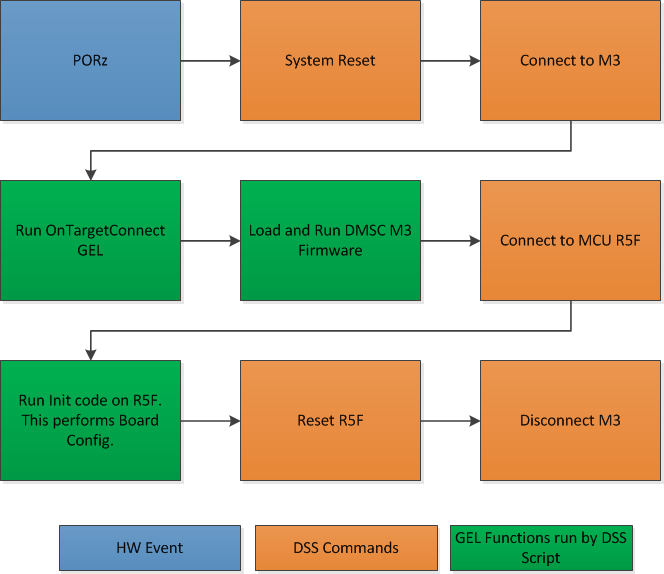
AM65x Advanced Debug Script Flow
5.2.1.3.3.1. Creating Debug Configuration to Integrate CCS GEL and DMSC Firmware Initialization
With the intent to maintain the same CCS target connect flow as existing devices, we provide a Debug Server Script (DSS) that users can link to in their target configuration to allow for loading SYSFW firmware on the DMSC as part of the target connect process.
The DSS script allows users to perform all of the initialization using a single click. When the script is run, the following actions happens sequentially:
- Running On Target Connect M3 existing GEL scripts.
- Loading the DMSC firmware
*.bin file to DMSC M3. - Run the R5F Init code which performs the board configuration initialization.
At the end of the setup, the R5F and A53 are in a clean state to load code and debug the application with the SYSFW loaded on the M3 core.
Steps to Link and Run the DSS Script for DMSC Firmware Loading
- Update the file “pdk/packages/ti/drv/sciclient/tools/ccsLoadDmsc/launch_am65xx.js” for the following variable to your PC location:
     //<!!!!!! EDIT THIS !!!!!>
     // Set this to 1 to allow loading the GEL files directly from the ccxml file.
     disableGelLoad = 1;
     if (disableGelLoad == 0)
     {
     //Path to GEL files
     gelFilePath = "C:/ti/ccsv8/ccs_base/emulation/gel/AM65xEVM";
     }
     // Path to the directory in which this file would be residing. CCS expects
     // absolute paths to load the binaries.
     thisJsFileDirectory = "pdk/packages/ti/drv/sciclient/tools/ccsLoadDmsc";
     //<!!!!!! EDIT THIS !!!!!>
- Set disableGelLoad =1 if GEL files is linked to the cores in the target configuration file.
- The variable “gelFilePath” doesn’t need to be updated if CCS is installed in the default C:/ti/ directory.
- The variable “thisJsFileDirectory” needs to be updated to point to the PDK install directory.
- Connect the Javascript to the CCXML file with the steps shown below.
Note
This step needs to be repeated if you switch workspaces or clean your workspace.
In the debug view after completing the basic CCS setup, Click on Debug Configurations from the button as show below:
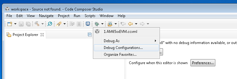
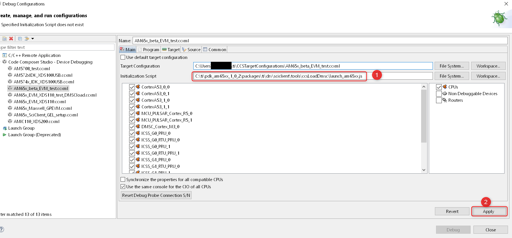
Select the CCXML file from the left-hand side and populate the path to the launch_am65xx.js file in the “Initialization Script” free form field and click on “Apply”.
Once you Launch the CCXML file, the java script will automatically run and connect to R5F.
Steps to re-run the script once ccxml is already launched:
In the CCS window, navigate to “View → Scripting Console.”
In the CCS Scripting Console, type:
> load ("<Your Path>\\launch_am65xx.js");
This would give the following output on the scripting console:
js:> load("C:\\Users\\User\\Documents\\PDK\\pdk\\packages\\ti\\drv\\sciclient\\tools\\ccsLoadDmsc\\launch_am65xx.js")
Connecting to DMSC_Cortex_M3_0!
Loading DMSC Firmware...
DMSC Firmware Load Done...
DMSC Firmware run starting now...
Connecting to MCU Cortex_R5_0!
GEL Output Log:
DMSC_Cortex_M3_0: GEL Output: Configuring AM65xEVM...
DMSC_Cortex_M3_0: GEL Output: Init value actual value: 0x00000888
DMSC_Cortex_M3_0: GEL Output: Register value: 0x00000888
DMSC_Cortex_M3_0: GEL Output: ATCM is on
DMSC_Cortex_M3_0: GEL Output: ATCM configured.
DMSC_Cortex_M3_0: GEL Output: Assuming execution from M3
DMSC_Cortex_M3_0: GEL Output: This script sets the first address translation region to [0x8000_0000, 0x0000_0000].
DMSC_Cortex_M3_0: GEL Output: It also sets the second address translation region to    [0x6000_0000, 0x4000_0000].
DMSC_Cortex_M3_0: GEL Output: Setting all PLLs in progress. This may take some time.
DMSC_Cortex_M3_0: GEL Output: 0 Percent Complete...
DMSC_Cortex_M3_0: GEL Output: 10 Percent Complete...
DMSC_Cortex_M3_0: GEL Output: 20 Percent Complete...
DMSC_Cortex_M3_0: GEL Output: 30 Percent Complete...
DMSC_Cortex_M3_0: GEL Output: 40 Percent Complete...
DMSC_Cortex_M3_0: GEL Output: 50 Percent Complete...
DMSC_Cortex_M3_0: GEL Output: 60 Percent Complete...
DMSC_Cortex_M3_0: GEL Output: 70 Percent Complete...
DMSC_Cortex_M3_0: GEL Output: 80 Percent Complete...
DMSC_Cortex_M3_0: GEL Output: 90 Percent Complete...
DMSC_Cortex_M3_0: GEL Output: Setting all PLLs done!
DMSC_Cortex_M3_0: GEL Output: Powering up all PSC power domains in progress...
DMSC_Cortex_M3_0: GEL Output: Powering up LPSC_WKUP_COMMON
DMSC_Cortex_M3_0: GEL Output: No change needed.
DMSC_Cortex_M3_0: GEL Output: Powering up LPSC_DMSC
DMSC_Cortex_M3_0: GEL Output: No change needed.
DMSC_Cortex_M3_0: GEL Output: Powering up LPSC_WKUP2MCU
DMSC_Cortex_M3_0: GEL Output: No change needed.
DMSC_Cortex_M3_0: GEL Output: Powering up LPSC_WKUP2MAIN_INFRA
DMSC_Cortex_M3_0: GEL Output: No change needed.
DMSC_Cortex_M3_0: GEL Output: Powering up LPSC_DEBUG2DMSC
DMSC_Cortex_M3_0: GEL Output: No change needed.
DMSC_Cortex_M3_0: GEL Output: Powering up LPSC_WKUP_GPIO
DMSC_Cortex_M3_0: GEL Output: No change needed.
DMSC_Cortex_M3_0: GEL Output: Powering up LPSC_MCU2MAIN_INFRA
DMSC_Cortex_M3_0: GEL Output: No change needed.
DMSC_Cortex_M3_0: GEL Output: Powering up LPSC_MCU2MAIN
DMSC_Cortex_M3_0: GEL Output: No change needed.
DMSC_Cortex_M3_0: GEL Output: Powering up LPSC_MCU2WKUP
DMSC_Cortex_M3_0: GEL Output: No change needed.
DMSC_Cortex_M3_0: GEL Output: Powering up LPSC_MAIN2MCU
DMSC_Cortex_M3_0: GEL Output: No change needed.
DMSC_Cortex_M3_0: GEL Output: Powering up LPSC_MCU_COMMON
DMSC_Cortex_M3_0: GEL Output: No change needed.
DMSC_Cortex_M3_0: GEL Output: Powering up LPSC_MCU_TEST
DMSC_Cortex_M3_0: GEL Output: No change needed.
DMSC_Cortex_M3_0: GEL Output: Powering up LPSC_MCU_MCAN_0
DMSC_Cortex_M3_0: GEL Output: No change needed.
DMSC_Cortex_M3_0: GEL Output: Powering up LPSC_MCU_MCAN_1
DMSC_Cortex_M3_0: GEL Output: No change needed.
DMSC_Cortex_M3_0: GEL Output: Powering up LPSC_MCU_OSPI_0
DMSC_Cortex_M3_0: GEL Output: No change needed.
DMSC_Cortex_M3_0: GEL Output: Powering up LPSC_MCU_OSPI_1
DMSC_Cortex_M3_0: GEL Output: No change needed.
DMSC_Cortex_M3_0: GEL Output: Powering up LPSC_MCU_HYPERBUS
DMSC_Cortex_M3_0: GEL Output: No change needed.
DMSC_Cortex_M3_0: GEL Output: Powering up LPSC_MCU_DEBUG
DMSC_Cortex_M3_0: GEL Output: No change needed.
DMSC_Cortex_M3_0: GEL Output: Powering up LPSC_MCU_R5_0
DMSC_Cortex_M3_0: GEL Output: No change needed.
DMSC_Cortex_M3_0: GEL Output: Powering up LPSC_MCU_R5_1
DMSC_Cortex_M3_0: GEL Output: No change needed.
DMSC_Cortex_M3_0: GEL Output: Powering up LPSC_MAIN_INFRA
DMSC_Cortex_M3_0: GEL Output: No change needed.
DMSC_Cortex_M3_0: GEL Output: Powering up LPSC_MAIN_TEST
DMSC_Cortex_M3_0: GEL Output: No change needed.
DMSC_Cortex_M3_0: GEL Output: Powering up LPSC_MAIN_PBIST
DMSC_Cortex_M3_0: GEL Output: No change needed.
DMSC_Cortex_M3_0: GEL Output: Powering up LPSC_CC_TOP
DMSC_Cortex_M3_0: GEL Output: No change needed.
DMSC_Cortex_M3_0: GEL Output: Powering up LPSC_A53_CLUSTER_0
DMSC_Cortex_M3_0: GEL Output: Power domain and module state changed successfully.
DMSC_Cortex_M3_0: GEL Output: Powering up LPSC_A53_0
DMSC_Cortex_M3_0: GEL Output: Power domain and module state changed successfully.
DMSC_Cortex_M3_0: GEL Output: Powering up LPSC_A53_1
DMSC_Cortex_M3_0: GEL Output: Power domain and module state changed successfully.
DMSC_Cortex_M3_0: GEL Output: Powering up LPSC_A53_CLUSTER_1
DMSC_Cortex_M3_0: GEL Output: Power domain and module state changed successfully.
DMSC_Cortex_M3_0: GEL Output: Powering up LPSC_A53_2
DMSC_Cortex_M3_0: GEL Output: Power domain and module state changed successfully.
DMSC_Cortex_M3_0: GEL Output: Powering up LPSC_A53_3
DMSC_Cortex_M3_0: GEL Output: Power domain and module state changed successfully.
DMSC_Cortex_M3_0: GEL Output: Powering up LPSC_MAIN_DEBUG
DMSC_Cortex_M3_0: GEL Output: No change needed.
DMSC_Cortex_M3_0: GEL Output: Powering up LPSC_DSS
DMSC_Cortex_M3_0: GEL Output: Power domain and module state changed successfully.
DMSC_Cortex_M3_0: GEL Output: Powering up LPSC_MMC
DMSC_Cortex_M3_0: GEL Output: Power domain and module state changed successfully.
DMSC_Cortex_M3_0: GEL Output: Powering up LPSC_CAL
DMSC_Cortex_M3_0: GEL Output: Power domain and module state changed successfully.
DMSC_Cortex_M3_0: GEL Output: Powering up LPSC_PCIE_0
DMSC_Cortex_M3_0: GEL Output: Power domain and module state changed successfully.
DMSC_Cortex_M3_0: GEL Output: Powering up LPSC_PCIE_1
DMSC_Cortex_M3_0: GEL Output: Power domain and module state changed successfully.
DMSC_Cortex_M3_0: GEL Output: Powering up LPSC_USB_0
DMSC_Cortex_M3_0: GEL Output: Power domain and module state changed successfully.
DMSC_Cortex_M3_0: GEL Output: Powering up LPSC_USB_1
DMSC_Cortex_M3_0: GEL Output: Power domain and module state changed successfully.
DMSC_Cortex_M3_0: GEL Output: Powering up LPSC_SAUL
DMSC_Cortex_M3_0: GEL Output: No change needed.
DMSC_Cortex_M3_0: GEL Output: Powering up LPSC_PER_COMMON
DMSC_Cortex_M3_0: GEL Output: No change needed.
DMSC_Cortex_M3_0: GEL Output: Powering up LPSC_NB
DMSC_Cortex_M3_0: GEL Output: No change needed.
DMSC_Cortex_M3_0: GEL Output: Powering up LPSC_SERDES_0
DMSC_Cortex_M3_0: GEL Output: Power domain and module state changed successfully.
DMSC_Cortex_M3_0: GEL Output: Powering up LPSC_SERDES_1
DMSC_Cortex_M3_0: GEL Output: Power domain and module state changed successfully.
DMSC_Cortex_M3_0: GEL Output: Powering up LPSC_ICSSG_0
DMSC_Cortex_M3_0: GEL Output: Power domain and module state changed successfully.
DMSC_Cortex_M3_0: GEL Output: Powering up LPSC_ICSSG_1
DMSC_Cortex_M3_0: GEL Output: Power domain and module state changed successfully.
DMSC_Cortex_M3_0: GEL Output: Powering up LPSC_ICSSG_2
DMSC_Cortex_M3_0: GEL Output: Power domain and module state changed successfully.
DMSC_Cortex_M3_0: GEL Output: Powering up LPSC_GPU
DMSC_Cortex_M3_0: GEL Output: Power domain and module state changed successfully.
DMSC_Cortex_M3_0: GEL Output: Powering up LPSC_EMIF_DATA
DMSC_Cortex_M3_0: GEL Output: Power domain and module state changed successfully.
DMSC_Cortex_M3_0: GEL Output: Powering up LPSC_EMIF_CFG
DMSC_Cortex_M3_0: GEL Output: Power domain and module state changed successfully.
DMSC_Cortex_M3_0: GEL Output: Powering up all PSC power domains done!
MCU_PULSAR_Cortex_R5_0: GEL Output: VTT Regulator Enabled
MCU_PULSAR_Cortex_R5_0: GEL Output:
PHY Init complete
MCU_PULSAR_Cortex_R5_0: GEL Output: DDRSS_DDRPHY_PGSR0 = 0x8000000F
MCU_PULSAR_Cortex_R5_0: GEL Output:
Waiting for DRAM Init to complete...
MCU_PULSAR_Cortex_R5_0: GEL Output:
DRAM Init complete
MCU_PULSAR_Cortex_R5_0: GEL Output: DDRSS_DDRPHY_PGSR0 = 0x8000001F
MCU_PULSAR_Cortex_R5_0: GEL Output:
Waiting for write leveling to complete
MCU_PULSAR_Cortex_R5_0: GEL Output:
Write leveling complete
MCU_PULSAR_Cortex_R5_0: GEL Output: DDRSS_DDRPHY_PGSR0 = 0x8000003F
MCU_PULSAR_Cortex_R5_0: GEL Output: checking status per byte...
MCU_PULSAR_Cortex_R5_0: GEL Output:
DDRSS_DDRPHY_DX0GSR0 = 0x00A728A0
MCU_PULSAR_Cortex_R5_0: GEL Output:
DDRSS_DDRPHY_DX1GSR0 = 0x00AA2920
MCU_PULSAR_Cortex_R5_0: GEL Output:
DDRSS_DDRPHY_DX2GSR0 = 0x00AB2920
MCU_PULSAR_Cortex_R5_0: GEL Output:
DDRSS_DDRPHY_DX3GSR0 = 0x00AA2A20
MCU_PULSAR_Cortex_R5_0: GEL Output:
Waiting for Read DQS training to complete
MCU_PULSAR_Cortex_R5_0: GEL Output:
Read DQS training complete
MCU_PULSAR_Cortex_R5_0: GEL Output: DDRSS_DDRPHY_PGSR0 = 0x8000007F
MCU_PULSAR_Cortex_R5_0: GEL Output: checking status per byte...
MCU_PULSAR_Cortex_R5_0: GEL Output:
DDRSS_DDRPHY_DX0RSR0 = 0x00000000
MCU_PULSAR_Cortex_R5_0: GEL Output:
DDRSS_DDRPHY_DX1RSR0 = 0x00000000
MCU_PULSAR_Cortex_R5_0: GEL Output:
DDRSS_DDRPHY_DX2RSR0 = 0x00000000
MCU_PULSAR_Cortex_R5_0: GEL Output:
DDRSS_DDRPHY_DX3RSR0 = 0x00000000
MCU_PULSAR_Cortex_R5_0: GEL Output:
Waiting for Write leveling adjustment to complete
MCU_PULSAR_Cortex_R5_0: GEL Output:
Write leveling adjustment complete
MCU_PULSAR_Cortex_R5_0: GEL Output: DDRSS_DDRPHY_PGSR0 = 0x800000FF
MCU_PULSAR_Cortex_R5_0: GEL Output:
Waiting for Read deskew to complete
MCU_PULSAR_Cortex_R5_0: GEL Output:
Read deskew complete
MCU_PULSAR_Cortex_R5_0: GEL Output: DDRSS_DDRPHY_PGSR0 = 0x800001FF
MCU_PULSAR_Cortex_R5_0: GEL Output:
Waiting for Write deskew to complete
MCU_PULSAR_Cortex_R5_0: GEL Output:
Write deskew complete
MCU_PULSAR_Cortex_R5_0: GEL Output: DDRSS_DDRPHY_PGSR0 = 0x800003FF
MCU_PULSAR_Cortex_R5_0: GEL Output:
Waiting for Read Eye training to complete
MCU_PULSAR_Cortex_R5_0: GEL Output:
Read Eye training complete
MCU_PULSAR_Cortex_R5_0: GEL Output: DDRSS_DDRPHY_PGSR0 = 0x800007FF
MCU_PULSAR_Cortex_R5_0: GEL Output:
Waiting for Write Eye training to complete
MCU_PULSAR_Cortex_R5_0: GEL Output:
Write Eye training complete
MCU_PULSAR_Cortex_R5_0: GEL Output: DDRSS_DDRPHY_PGSR0 = 0x80000FFF
MCU_PULSAR_Cortex_R5_0: GEL Output:
Waiting for VREF training to complete
MCU_PULSAR_Cortex_R5_0: GEL Output:
VREF training complete
MCU_PULSAR_Cortex_R5_0: GEL Output: DDRSS_DDRPHY_PGSR0 = 0x80004FFF
MCU_PULSAR_Cortex_R5_0: GEL Output:

====

DDR4 Initialization has PASSED!!!!

====
5.2.1.3.3.2. Additional Notes for GEL Users
R5F in Split Mode Configuration
AM65x EVM ships with the dual Cortex R5F configured in lockstep mode. The AM65x EVM GEL file provides a GEL function “Change_MCUSS_to_SplitMode” that can be added to OnTargetConnect or invoked from the DMSC_Cortex_M3 to set the dual R5F in split mode.
Configuring PRU-ICSS in Sync Mode
The PRU-ICSS subsystem can be configured to SYNC mode (250 Mhz) using the GEL function “PRU_ICSSG_SyncMode_250MHz” from Cortex A53 or R5F