6.1.14. AM335x to AM437x Hardware Migration Guide
6.1.14.1. Introduction
This document explains the differences between the TI AM335x processor and the TI AM437x processor. All of the documentation referenced in this migration guide can be found on the TI website located in the two device respective product folders. The device folders are found at the following web pages.
6.1.14.2. Basic Feature Comparison
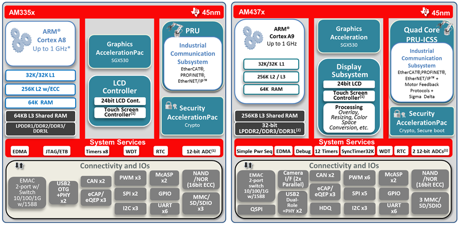
The figure and table below show a comparison of the basic features of the AM335x and the AM437x. The remainder of the document presents a comparison of these features in greater detail, and also provides references to the appropriate documentation for further information.
| Device Family | AM335x | AM437x |
|---|---|---|
| Device |
|
|
| Package Options | ||
| Packages |
|
|
| Co-processors and Subsystems | ||
| ARM Processor |
Supported OPP: 50%/100%/120%/Turbo/Nitro |
Supported OPP: 50%/100%/120%/Turbo/Nitro |
| Neon Co-processor | Y | Y |
| Graphics Engine | 3SGX530 3D, 200 MHz | SGX530 3D, 200 MHz |
| System DMA | eDMA | eDMA |
| PRU-ICSS | 1 | 2 |
| Memory Interfaces | ||
| mDDR/DDR2/DDR3 Controller |
|
|
| GPMC | Y | Y |
| ELM | Y | Y |
| On Chip Memory (OCMC) | 64KB (general purpose) | 256KB (general purpose) |
| Security | ||
| Crypto hardware accelerators | Y | Y |
| Video Interfaces | ||
| Camera ISP / VPFE | N | Y |
| Display | LCD Controller | Display Subsystem (DSS) |
| Peripherals | ||
| USB | Two (2) USB 2.0 High Speed ports with integrated PHY (13 x 13 Package has only one USB port) | Two (2) USB 2.0 High Speed ports with integrated PHY |
| eMAC | 2 (10/100/1000 Mbps) | 2 (10/100/1000 Mbps) |
| CAN | 2 | 2 |
| McASP | 2 | 2 |
| UART | 6 (all with IrDA) | 6 (all with IrDA) |
| McSPI | 2 | 5 |
| QSPI | not present | 1 |
| I2C | 3 | 3 |
| GPIO | 4 banks | 6 banks |
| eCAP | 3 | 3 |
| eHRPWM | 3 | 6 |
| eQPE | 3 | 3 |
| ADC | 1 (TSC/ADC) | 2 (1 TSC/ADC and 1 ADC) |
| Removable Media | ||
| MMC/SD/SDIO | 3 | 3 |
| D1W/HDQ | N | Y |
| Power, Reset and Clock Management | ||
| RTC | Y | Y |
| Test Interfaces | ||
| JTAG | Y | Y |
| ETM, PTM, & ETB | ETM & ETB | PTM |
| IEEE 1500 support | Y | Y |
| RTT | N | Y |
| Misc | ||
| GP Timer | 7 | 12 |
| Watchdog Timer | 1 | 1 |
6.1.14.3. Module Comparison
6.1.14.3.1. Processors
6.1.14.3.1.1. ARM Core
AM335x is based on the ARM Cortex-A8 processor. AM437x is based on the ARM Cortex-A9 processor. The table below shows a comparison between these two devices.
| ARM Processor | AM335x | AM437x |
| ARM Processor | ARM Cortex™ A8 | ARM Cortex™ A9 |
| Revision | r3p2 | r2p10 |
| Operating Performance Points | OPP50, OPP100, OPP120, Turbo, Nitro | OPP50, OPP100, OPP120, Turbo, Nitro |
| Operating Voltages | .95V, 1.1V, 1.2V, 1.26V, 1.325V | .95V, 1.1V, 1.2V, 1.26V, 1.325V |
| Operating Frequencies | 300MHz, 600MHz, 720MHz, 800MHz, 1000MHz | 300MHz, 600MHz, 720MHz, 800MHZ, 1000MHz |
| L1 Instruction Cache | 32 Kbytes | 32 Kbytes |
| L1 Data Cache | 32 Kbytes | 32 Kbytes |
| L1 with PED | Yes | Yes |
| L2 Cache | 256 Kbytes | 256 Kbyte |
| L2 with ECC | Yes | No |
| ROM Size | 176 Kbytes | 64 Kbytes |
| RAM Size | 64 Kbytes | 64 Kbytes |
Note: Please refer to the AM335x and AM437x Datasheets for the latest OPP values.
6.1.14.3.1.2. Neon Co-processor
The Neon co-processor is the same between the two devices.
6.1.14.3.1.3. Graphics Engine
The SGX530 3D Graphics Engine is the same between both devices.
6.1.14.3.1.4. System DMA
AM437x has a new DMA event mapping corresponding to the supported peripherals on this device. Additionally, AM335x has 32 events in the cross bar and AM437x has 64.
6.1.14.3.1.5. On-Chip Memory
AM335x has 64KB of general purpose on-chip memory controller (OCMC) RAM. AM437x has 256KB of general purpose on-chip memory controller (OCMC) RAM.
6.1.14.3.2. Memory Subsystem
6.1.14.3.2.1. General Purpose Memory Controller
Both AM335x and AM437x support 7 chip selects.
6.1.14.3.2.2. External Memory Interface
AM335x supports a single 16-bit LPDDR (mDDR)/DDR2/DDR3 SDRAM Interface, with up to:
- LPDDR 200-MHz Clock (400-MHz Data Rate)
- DDR2 266-MHz Clock (532-MHz Data Rate)
- DDR3 400-MHz Clock (800-MHz Data Rate)
- DDR3L 400-MHz Clock (800-MHz Data Rate)
One x32 device or two x16 devices and 1 GB (total) of address space are supported.
AM437x supports a single 32-bit LPDDR2(discrete or non-POP)/DDR3L/DDR3 SDRAM Interface, with up to:
- LPDDR2: 266-MHz Clock (LPDDR2-533 Data Rate)
- DDR3: 400-MHz Clock ( DDR3-800 Data Rate)
- DDR3L: 400-MHz Clock (DDR3L-800 Data Rate)
One x32 device, two x16 devices, or four 8x devices and 2 GB (total) of address space are supported.
6.1.14.3.3. Power, Reset, and Clock Management
6.1.14.3.3.1. Operating Performance Points
| OPP | ARM Frequency (MHz) | Voltage (V) |
| Nitro | 1000 | 1.325 |
| Turbo | 800 | 1.26 |
| OPP120 | 720 | 1.20 |
| OPP100 | 600 | 1.10 |
| OPP50 | 300 | 0.95 |
Note: Please refer to the AM335x and AM437x Datasheets for the latest OPP values.
6.1.14.3.3.2. Voltage Rails
The following table compares the power supplies for AM335x and AM437x:
Table: AM335x Voltage Rails
| SIGNAL | DESCRIPTION | VALUE |
| VDD_CORE | Core domain | 1.1V |
| VDD_MPU * | MPU domain | 0.95V - 1.26V |
| CAP_VDD_RTC | RTC domain input/LDO output | 1.1V |
| VDDS_RTC | RTC domain | 1.8V |
| VDDS_DDR | DDR IO domain (DDR2 / DDR3) | 1.8V / 1.5V |
| VDDS | Dual voltage IO domains | 1.8V |
| VDDS_SRAM_CORE_BG | Core SRAM LDOs, Analog | 1.8V |
| VDDS_SRAM_MPU_BB | MPU SRAM LDOs, Analog | 1.8V |
| VDDS_PLL_DDR | DPLL DDR, Analog | 1.8V |
| VDDS_PLL_CORE_LCD | DPLL Core and LCD, Analog | 1.8V |
| VDDS_PLL_MPU | DPLL MPU, Analog | 1.8V |
| VDDS_OSC | System oscillator IOs, Analog | 1.8V |
| VDDA1P8V_USB0 | USB PHY, Analog, 1.8V | 1.8V |
| VDDA1P8V_USB1 | USB PHY, Analog, 1.8V | 1.8V |
| VDDA3P3V_USB0 | USB PHY, Analog, 3.3V | 3.3V |
| VDDA3P3V_USB1 | USB PHY, Analog, 3.3V | 3.3V |
| VDDA_ADC | ADC, Analog | 1.8V |
| VDDSHV1 | Dual Voltage IO domain (1.8-V operation) | 1.8V |
| VDDSHV2 * | Dual Voltage IO domain (1.8-V operation) | 1.8V |
| VDDSHV3 * | Dual Voltage IO domain (1.8-V operation) | 1.8V |
| VDDSHV4 | Dual Voltage IO domain (1.8-V operation) | 1.8V |
| VDDSHV5 | Dual Voltage IO domain (1.8-V operation) | 1.8V |
| VDDSHV6 | Dual Voltage IO domain (1.8-V operation) | 1.8V |
| VDDSHV1 | Dual Voltage IO domain (3.3-V operation) | 3.3V |
| VDDSHV2 * | Dual Voltage IO domain (3.3-V operation) | 3.3V |
| VDDSHV3 * | Dual Voltage IO domain (3.3-V operation) | 3.3V |
| VDDSHV4 | Dual Voltage IO domain (3.3-V operation) | 3.3V |
| VDDSHV5 | Dual Voltage IO domain (3.3-V operation) | 3.3V |
| VDDSHV6 | Dual Voltage IO domain (3.3-V operation) | 3.3V |
| DDR_VREF | DDR SSTL/HSTL reference input (DDR2/DDR3) | 0.50*VDDS_DDR |
| USB0_VBUS | USB VBUS comparator input | |
| USB1_VBUS | USB VBUS comparator input | |
| USB0_ID | USB ID input | 1.8V |
| USB1_ID | USB ID input | 1.8V |
* Note: These voltage rails are not available in the 13x13 package.
Table: AM437x Voltage Rails
| SIGNAL | DESCRIPTION | VALUE |
| VDD_CORE | Core domain | TBD * |
| VDD_MPU | MPU domain | TBD * |
| CAP_VDD_RTC | RTC domain input/LDO output | 1.1V |
| VDDS_RTC | RTC domain | 1.8V |
| VDDS_DDR | DDR IO domain (DDR2 / DDR3) | 1.2V - 1.5V |
| VDDS | Dual voltage IO domains | 1.8V |
| VDDS_SRAM_CORE_BG | Core SRAM LDOs, Analog | 1.8V |
| VDDS_SRAM_MPU_BB | MPU SRAM LDOs, Analog | 1.8V |
| VDDS_PLL_DDR | DPLL DDR, Analog | 1.8V |
| VDDS_PLL_CORE_LCD | DPLL Core and LCD, Analog | 1.8V |
| VDDS_PLL_MPU | DPLL MPU, Analog | 1.8V |
| VDDS_OSC | System oscillator IOs, Analog | 1.8V |
| VDDA1P8V_USB0 | USB PHY, Analog, 1.8V | 1.8V |
| VDDA1P8V_USB1 | USB PHY, Analog, 1.8V | 1.8V |
| VDDA3P3V_USB0 | USB PHY, Analog, 3.3V | 3.3V |
| VDDA3P3V_USB1 | USB PHY, Analog, 3.3V | 3.3V |
| VDDA_ADC0 | ADC0, Analog | 1.8V |
| VDDA_ADC1 | ADC1 | 1.8V |
| VDDSHV1 | Dual Voltage IO domain (1.8V/3.3V operation) | 1.8V/3.3V |
| VDDSHV2 | Dual Voltage IO domain (1.8V/3.3V operation) | 1.8V/3.3V |
| VDDSHV3 | Dual Voltage IO domain (1.8V/3.3V operation) | 1.8V/3.3V |
| VDDSHV4 | Dual Voltage IO domain (1.8V/3.3V operation) | 1.8V/3.3V |
| VDDSHV5 | Dual Voltage IO domain (1.8V/3.3V operation) | 1.8V/3.3V |
| VDDSHV6 | Dual Voltage IO domain (1.8V/3.3V operation) | 1.8V/3.3V |
| VDDSHV7 | Dual Voltage IO domain (1.8V/3.3V operation) | 1.8V/3.3V |
| VDDSHV8 | Dual Voltage IO domain (1.8V/3.3V operation) | 1.8V/3.3V |
| VDDSHV9 | Dual Voltage IO domain (1.8V/3.3V operation) | 1.8V/3.3V |
| VDDSHV10 | Dual Voltage IO domain (1.8V/3.3V operation) | 1.8V/3.3V |
| VDDSHV11 | Dual Voltage IO domain (1.8V/3.3V operation) | 1.8V/3.3V |
| DDR_VREF | DDR SSTL/HSTL reference input (DDR2/DDR3) | 0.50*VDDS_DDR |
| USB0_VBUS | USB VBUS comparator input | |
| USB1_VBUS | USB VBUS comparator input | |
| USB0_ID | USB ID input | 1.8V |
| USB1_ID | USB ID input | 1.8V |
* Note: Please refer to the AM437x Datasheet for the latest values.
6.1.14.3.3.3. Input Clocks
Table: AM335x Input Clocks
| CLOCK NAME | SOURCE | VALUE |
| CLK_M_OSC | Master Oscillator | 19.2, 24, 25, 26 MHz |
| CLK_32KHZ | Divide down of PER PLL output (PLL uses Master Osc) | 32768 Hz Precise |
| CLK_RC_32KHZ | Internal RC Oscillator | 16 - 60 kHz |
| CLK_32K_RTC | External 32768 Hz crystal with internal 32K Osc or external 32768 Hz clock | 32768 Hz Precise |
Table: AM437x Input Clocks
| CLOCK NAME | SOURCE | VALUE |
| CLK_M_OSC | Master Oscillator | 19.2, 24, 25, 26 MHz |
| CLK_32KHZ | Divide down of PER PLL output (PLL uses Master Osc) | 32768 Hz Precise |
| CLK_RC_32KHZ | Internal RC Oscillator | 16 - 60 kHz |
| CLK_32K_RTC | External 32768 Hz crystal with internal 32K Osc or external 32768 Hz clock | 32768 Hz Precise |
| CLK_32K_MOSC | Divide down of Master Oscillator Crystal Frequency | Precise 32768 Hz only when using 26 MHz crystal |
6.1.14.3.3.4. PLLs
AM335x has the following PLLs, driven by a crystal (CLK_M_OSC):
- Core PLL - for SGX, EMAC, L3S, L3F, L4F, L4_PER, L4_WKUP, PRU-ICSS IEP, Debugss
- Peripheral (Per) PLL - for USB PHY, PRU-ICSS UART, MMC/SD, SPI, I2C, UART
- MPU PLL - for MPU Subsystem (includes Cortex A-8)
- Display PLL - for LCD Pixel Clock
- DDR PLL - for EMIF
AM437x has the following PLLs, driven by a crystal (CLK_M_OSC):
- Core PLL - for SGX, L3S, L3F, L4F, L4F_PER, PRU_ICSS_IEP, Debugss, GEMAC, PRU_ICSS OCP
- Peripheral (Per) PLL - for PRU_ICSS_UART, MMC/SD, SPI, UART, I2C
- MPU PLL - for MPU Subsystem (includes Cortex A-9)
- Display PLL - for LCD Pixel Clock
- DDR PLL - for EMIF
6.1.14.3.3.5. Power Management Feature Comparison
| HW Provisions for Power Optimization/ Control | AM335x | AM437x |
| Individually Switchable Power Domains | Full support for Individual Power Domain ON/OFF: VDD_MPU, VDD_CORE, VDD_PER, VDD_SGX and SRAMs. In RTC_Only mode, even WAKEUP Domain can be OFF’d | Full support for Individual Power Domain ON/OFF: VDD_MPU, VDD_CORE, VDD_PER, VDD_SGX and SRAMs. |
| Dynamically gating OFF of Clocks to one/more of groups of modules (clock domains) when inactive to conserve power | Supported | Supported |
| Operating Voltage-Frequencies (OPPs) | OPP100(VDD_MPU, VDD_CORE), OPP50(VDD_MPU, VDD_CORE), OPP120 (VDD_MPU), OPP1G (VDD_MPU) | OPP50 (VDD_CORE, VDD_MPU), OPP100 (VDD_CORE, VDD_MPU), OPP120 (VDD_MPU), Turbo (VDD_MPU), Nitro (VDD_MPU) |
| Adaptive Voltage Scaling | Class 2B Smart Reflex, VDD_CORE & VDD_MPU can be scaled. VDD_RTC is Fixed. | Not supported |
| SRAM memory retention | All onchip SRAMs | Supported on all memories |
| HW Auto Clock/Power Domain Dependency Management | Not Supported | Not Supported |
| Low Power Deep-Sleep State w/ Auto Wakeup | GPIO0 bank, UART0, RTC, I2C0, DMTimer 1ms, USB Resume and TSC/ ADC Control events | GPIO0, Timers, USB resume, RTC, UART, TSC, ADC0, Not supporting wakeup from any IO |
| RTC Only Cold State | Supported. System includes 32KHz Osc integrated with alarm/wake signaling interface w/ PMIC. | Supported |
| Splitting Of Primary Voltage Supply Rails | VDD_CORE, VDD_MPU*, VDD_RTC | VDD_CORE, VDD_MPU |
* On 13x13 mm package option, VDD_CORE and VDD_MPU are merged.
6.1.14.3.3.6. Bootmodes
| AM335x | AM437x | Boot Type | Description |
| Y | Y | NOR | This mode allows booting from XIP booting devices, such as NOR flash memories. For AM355x, NOR Flash (up to 1 Gb, or 128M bytes) should be connected to the GPMC peripheral on GPMC_CSn0. GPMC_CSn0 is mapped to address 0x8000_0000. A data bus width of x8 or x16 is supported. The GPMC is clocked at 50MHz. For AM437x, NOR Flash (up to 1 Gb, or 128M bytes) should be connected to the GPMC peripheral on GPMC_CSn0. GPMC_CSn0 is mapped to address 0x8000_0000. A data bus width of x16 supported(x8 not supported). The GPMC is clocked at 50MHz. Wait monitoring is also supported and enabled/disabled based on SYSBOOT pins. |
| Y | Y | NAND | This mode starts downloading code from an NAND memory. For AM335x, NAND flash (from 512Mbit, or 64Mbytes)should be connected to the GPMC peripheral on GPMC_CSn0. GPMC_CSn0 is mapped to address 0x8000_0000. A data bus width of x16 is supported. The GPMC is clocked at 50MHz. For AM437x, NAND flash (from 512Mbit, or 64Mbytes)should be connected to the GPMC peripheral on GPMC_CSn0. GPMC_CSn0 is mapped to address 0x8000_0000. A data bus width of x16 or x8 is supported. The GPMC is clocked at 50MHz. |
| Y | Y | SPI | This mode starts downloading code from an SPI EEPROM or SPI Flash. For both AM335x and AM437x, the SPI device should be connected to the SPI0 peripheral on CS0. |
| N | Y | QSPI | This mode starts downloading code from Quad SPI Flash. For AM437x, the QSPI device should be connected to the QSPI peripheral on CS0. |
| Y | Y | UART | In this mode, the UART sends a BOOTME request to the UART peripheral and waits for a response along with code from a host processor. AM335x must be booted using a baud rate of 115200. Both devices can only boot from UART0. For AM437x, must be booted using a baud rate of 115200, 8-bit, no parity, 1 stop bit and noflow control. Both devices can only boot from UART0. |
| Y | Y | MMCSD | This mode starts booting code from an MMC/SD Controller. For AM335x, an MMC/SD card can be connected to the MMC0 interface typically through a card cage. An eMMC/eSD/managed NAND memory device can be connected to MMC1 interface. 1.8V or 3.3V I/O voltage is supported on both MMC0 and MMC1. For AM437x, an MMC/SD card or eMMC/eSD/managed NAND memory device can connect to MMC0 or MMC1 interface. Support for 3.3 V or 1.8 V I/O voltages. NOTE For MMC1, the boot ROM is configuring a different set of pins to operate as the MMC1 interface. AM335x boot ROM configures gpmc_ad[3:0] as mmc1_dat[3:0]. The AM437x boot ROM configures gpmc_ad[11:8] as mmc1_dat[3:0]. |
| Y | Y | EMAC | This mode starts booting code from the EMAC port. For both AM335x and AM437x, EMAC boot uses the CPGMAC port 1 of the device. |
| N | Y | USB | This mode starts booting code from the USB device. For AM437x, two USB boot modes are supported:
Note that USB boot is not supported with AM437x PG1.1. SuperSpeed devices will enumerate and function as High-Speed devices. |
6.1.14.3.4. Multimedia Hardware Components
6.1.14.3.4.1. LCDC vs DSS
The below image provides a brief summary of the differences between LCDC and DSS. Please refer to the TRM for more information.

6.1.14.3.4.2. DSS FIFO Underflow
6.1.14.3.4.2.1. Introduction
In order to prevent DSS underflows, system level tuning is required; the errata describes the exact nature of this tuning process. For an in-depth description of the FIFO Underflow condition, refer to the AM437x Silicon Errata Advisory 14: AM437x Silicon Errata
In linux, there are a couple of events that will indicate that a DSS underflow has occurred:
- The kernel will dump a warning message along the lines of GFX FIFO UNDERFLOW, which means that the underflow occurred in the FIFO that feeds the Graphics Plane of the DSS.
- On the display screen, white flickering lines will appear .
6.1.14.3.4.2.2. Tuning the System
Adjusting the parameters described in the errata will usually take place in u-boot. As an experiment, users could add the below lines in the uEnv.txt file to modify the Uboot registers:
# Set Output Resolution
optargs=video=HDMI-A-1:800x600

# A9 limiter = 700MBPS
a9_limiter=mw.l 0x44005208 0x10; md 0x44005208 0x1; mw.l 0x4400520C 0x3; md 0x4400520C 0x1; mw.l 0x44005210 0x0; md 0x44005210 1

# EMIF COS
# mw.l 0x4C000108 0x80000000;
emif_cos=mw.l 0x4C000120 0x80000405; md 0x4C000120 1; mw.l 0x4C000104 0x80000094; md 0x4C000104 1; md 0x4C000108 1; mw.l 0x4C000100 0x80000009; md 0x4C000100 1; mw.l 0x4C000124 0x000FFFFF; md 0x4C000124 1

# DSS MREQ Prio
mreq_prio=mw.l 0x44E10670 0x44444477; md 0x44E10670 1; mw.l 0x44E10674 0x00444400; md 0x44E10674 1

uenvcmd= run a9_limiter; run emif_cos; run mreq_prio;
However, above changes are already integrated in the PSDK Uboot. Please refer to the following patch. We recommend to set the appropriate values in the the Uboot code as opposed to the text file.
6.1.14.3.4.2.3. FIFOMERGE
One other way to greatly reduce the DSS susceptibility to underflows is to enable FIFOMERGE; this combines the three 1kB FIFOs that feed the Graphics Plane and both Video Planes of the DSS into one larger 3 kB FIFO. The downside to this is that only one plane of the DSS can be used at a time, which essentially disables all blending and makes scaling less useful. A strong benefit of FIFOMERGE is that allows for reduced restrictions on the ARM bandwidth for all resolutions.
If you are using fbdev, here is a patch that shows how to merge the FIFO:
diff --git a/drivers/video/fbdev/omap2/omapfb/dss/apply.c b/drivers/video/fbdev/omap2/omapfb/dss/apply.c
index 2481f4871f..46b68b21df 100644
--- a/drivers/video/fbdev/omap2/omapfb/dss/apply.c
+++ b/drivers/video/fbdev/omap2/omapfb/dss/apply.c
@@ -1039,6 +1039,10 @@ static void dss_ovl_setup_fifo(struct omap_overlay *ovl)

        if (!op->enabled && !op->enabling)
                return;
+       if (dss_has_feature(FEAT_FIFO_SZ_LIMITATION)) {
+               use_fifo_merge = true;
+               dispc_enable_fifomerge(use_fifo_merge);
+       }

        dispc_ovl_compute_fifo_thresholds(ovl->id, &fifo_low, &fifo_high,
                        use_fifo_merge, ovl_manual_update(ovl));
diff --git a/drivers/video/fbdev/omap2/omapfb/dss/dispc.c b/drivers/video/fbdev/omap2/omapfb/dss/dispc.c
index a06d9c2576..e6292a856c 100644
--- a/drivers/video/fbdev/omap2/omapfb/dss/dispc.c
+++ b/drivers/video/fbdev/omap2/omapfb/dss/dispc.c
@@ -1329,7 +1329,7 @@ void dispc_ovl_compute_fifo_thresholds(enum omap_plane plane,
                *fifo_low = 0;
                *fifo_high = burst_size;
        } else {
-               *fifo_low = ovl_fifo_size - burst_size;
+               *fifo_low = total_fifo_size - burst_size;
                *fifo_high = total_fifo_size - buf_unit;
        }
 }
diff --git a/drivers/video/fbdev/omap2/omapfb/dss/dss_features.c b/drivers/video/fbdev/omap2/omapfb/dss/dss_features.c
index e8d428bc47..6cffe132dc 100644
--- a/drivers/video/fbdev/omap2/omapfb/dss/dss_features.c
+++ b/drivers/video/fbdev/omap2/omapfb/dss/dss_features.c
@@ -521,6 +521,7 @@ static const enum dss_feat_id am43xx_dss_feat_list[] = {
        FEAT_FIR_COEF_V,
        FEAT_ALPHA_FIXED_ZORDER,
        FEAT_FIFO_MERGE,
+       FEAT_FIFO_SZ_LIMITATION,
 };

 static const enum dss_feat_id omap3630_dss_feat_list[] = {
diff --git a/drivers/video/fbdev/omap2/omapfb/dss/dss_features.h b/drivers/video/fbdev/omap2/omapfb/dss/dss_features.h
index 3d67d39f19..433d925662 100644
--- a/drivers/video/fbdev/omap2/omapfb/dss/dss_features.h
+++ b/drivers/video/fbdev/omap2/omapfb/dss/dss_features.h
@@ -62,6 +62,9 @@ enum dss_feat_id {
        FEAT_BURST_2D,
        FEAT_DSI_PHY_DCC,
        FEAT_MFLAG,
+       /* When DSS has to be used with all FIFO's merged */
+    +   /* due to bandwidth constraints */
+    +   FEAT_FIFO_SZ_LIMITATION,
 };

 /* DSS register field id */
If FIFOMERGE is used, the DSS becomes limited in its ability to blend graphics and video data. Either the user must perform color space conversion using the ARM core, or the color space of the camera data must match the color space of the framebuffer before blending. Another possibility is to develop an OpenGL based application that uses the SGX core for blending and color space conversion.
This table lists different bandwidth restrictions that are needed based on what resolution is desired.
| Resolution | ARM BW Limit (MB/s) |
|---|---|
| 1920x1080p30 | 300 |
| 1280x720p60 | 300 |
| 1024x768p60 | 700 |
| 800x480p60 | 700 |
| 640x480p60 | 900 |
6.1.14.3.5. Communication Interfaces
6.1.14.3.5.1. MMC/SD
The MMC/SD modules are binary compatible between the two devices. Except, the CLK32 debounce clock is created by dividing the 96-MHz (48-MHz in AM437x) clock in the PRCM by two and then dividing the resulting 48-MHz (24-MHz in AM437x) clock by a fixed 732.4219 in the Control Module to get a 32-kHz clock.
| FEATURE | AM335x | AM437x |
| Spec Compliance | MMC v4.3 SD Phys Layer v3.0 SDIO v2.0 SD card v2.0 | MMC v4.3 SD Phys Layer v3.0 SDIO v2.0 SD card v2.0 |
| Data Width * | 8-bit (MMC0/1/2) | 8-bit (MMC0/1/2) |
| Max Clock Rate | 48MHz (MCC), 48MHz (SD), 48MHz (SD) | 48MHz (MCC), 48MHz (SD), 48MHz (SD) |
* Note the supported data width is subject to pinmux constraints.
6.1.14.3.5.2. USB
The AM335x has 2 MUSB controllers that have a USB port capable of host and OTG operations and have an integrated PHY that supports HS, FS and LS. The AM437x contains two USB 2.0 dual-role-device (DRD) subsystems, either of which can be configured as an xHCI Host (HS, FS, LS supported) or as a Device (HS and FS supported).
6.1.14.3.5.3. I2C
The I2C ports are binary compatible between the two devices. Both devices support 3 general I2C ports. The ports only support 100/400Kbps operation. No high speed mode is supported.
6.1.14.3.5.4. UART
On AM335x and AM437x, only UART1 supports full modem control. All 6 UARTs support a maximum baud rate of 3.6864 Mbps.
The UART interface clock (CLK) is sourced from CORE_CLKOUTM4 / 2 in AM335x and AM437x (max 100-MHz) except for UART0 on AM437x that is sourced from M_OSC_CLK in AM437x (max 26-MHz).
6.1.14.3.5.5. Real-Time Clock (RTC)
The RTC module is identical between the two devices, except for the interface clock source – AM335x uses CORE_CLKOUTM4/2, providing a max frequency of 100 MHz. AM437x uses CLK_M_OSC, providing a max frequency of 26 MHz.
6.1.14.3.5.6. Ethernet
There are small differences between the AM335x and AM437x Ethernet module.
The AM437x module adds support for multi core split processing, connecting the Core 0 interrupt to the MPU subsystem and the Core 2 interrupt to the PRU-ICSS. On AM335x, the Core 0 interrupt was connected to both the MPU subsystem and the PRU-ICSS. Core 1 and Core 2 interrupts were unconnected.
In AM437x, the cpts_rft_clk (IEEE 1588v2 clock) adds DISP_PLL_CLK as a third source option.
6.1.14.3.5.7. McSPI
AM335x includes 2 McSPI ports, each with two chip select signals. All McSPI have 4 DMA requests to EDMA.
AM437x includes 5 McSPI ports. McSPI[0-2] support 4 chip select signals and 8 DMA requests to the eDMA. McSPI[3-4] only support 2 CS signals and 4 DMA requests to the eDMA.
6.1.14.3.5.8. PWM Subsystem (PWMSS)
The PWM Subsystem contains PWM, eCAP, and eQEP submodules. AM335x has 3 PWMSS instances. AM437x has 6 PWMSS instances, but eCAP3-5 and eQEP3-5 are not used.
The PWMSS synchronization of the PWM and eCAP submodules is also different between AM335x and AM437x.
6.1.14.3.5.9. PRU-ICSS - Programmable Real-time Unit Subsystem and Industrial Communications Subsystem
AM335x has one PRU-ICSS and AM437x has two PRU-ICSS. The PRU-ICSS on AM437x is backwards compatible with the subsystem on AM335x. The table below summarizes the differences between the PRU-ICSS instances on each device.
| Features | AM335x PRU-ICSS1 |
AM437x PRU-ICSS1 |
AM437x PRU-ICSS0 |
| Number of PRU cores | 2 | 2 | 2 |
| Frequency | 200 MHz | 200 MHz | 200 MHz |
| IRAM size (per PRU core) | 8 KB | 12 KB | 4 KB |
| DRAM size (per PRU core) | 8 KB | 8 KB | 4 KB |
| Shared DRAM size | 12 KB | 32 KB | 0 KB |
| General Purpose Input (per PRU core) | Direct; or 16-bit parallel capture; or 28-bit shift | 3Direct; or 16-bit parallel capture; or 28-bit shift | Direct; or 16-bit parallel capture; or 28-bit shift |
| General Purpose Output (per PRU core) | Direct; or Shift out | Direct; or Shift out | Direct; or Shift out |
| GPI Pins (PRU0, PRU1) | 17, 17 | 13, 0 | 20, 20 |
| GPO Pins (PRU0, PRU1) | 16, 16 | 12, 0 | 20, 20 |
| Scratchpad | Y (3 banks) | Y (3 banks) | N |
| INTC | 1 | 1 | 1 |
| UART | 1 | 1 | 1 |
| eCAP | 1 | 1 | not connected |
| IEP | 1 | 1 | not connected |
| MII_RT | 2 | 2 | not connected |
| MDIO | 1 | 1 | not connected |
6.1.14.3.6. Timers
6.1.14.3.6.1. GPTimer
AM335x has 7 General Purpose Timers. One GPTimer (DMTIMER1) is specialized for accurate 1mS OS Ticks. Only 4 GPTimers (DMTIMER4 - DMTIMER7) are extended to SoC pins.
AM437x has 12 General Purpose Timers. One GPTimer (DMTIMER1) is specialized for accurate 1mS OS Ticks. Only 6 GPTimers (DMTIMER0, DMTIMER1, DMTIMER4 - DMTIMER7) are extended to SoC pins. AM437x also adds support for timer cascading, providing a 64-bit timer option. With this feature, DMTIMER2-3 provide a 64-bit internal timer and DMTIMER4-5 provide a 64-bit timer with output capability.
6.1.14.3.6.2. WDTimer
AM335x and AM437x both have one watchdog timer.
Additionally, the interface clock source is different between the two devices. AM335x uses CORE_CLKOUTM4/2, providing a max frequency of 100 MHz. AM437x uses CLK_M_OSC, providing a max frequency of 26 MHz.
6.1.14.3.7. Misc
6.1.14.3.7.1. GPIOs
AM335x has 4 banks of GPIOs, each with 32 dedicated IO pins. With the 4 GPIO modules, AM335x allows for a maximum of 128 GPIO pins. Supports a single DMA request for GPIO[0:2].
AM437x has 6 banks of GPIOs, each with 32 dedicated IO pins. With the 6 GPIO modules, AM437x allows for a maximum of 192 GPIO pins. Supports a single DMA request for each GPIO module.
6.1.14.3.8. ARM Interrupt Controller
AM335x and AM437x implement different interrupt controllers. Additionally, the interrupt controller on AM335x has 128 interrupt lines. AM437x has 224 interrupt lines.
6.1.14.3.9. New interfaces in AM437x
The following are new interfaces in the AM437x device that do not exist in AM335x. Any details about these interfaces can be found in the Technical Reference Manual for AM437x.
- Camera Video Processing Front End (VPFE)
- Quad-SPI (QSPI)
- Dallas1-Wire & HDQ
- Generic ADC
6.1.14.3.10. Pin and package
The AM335x and the AM437x devices are offered different mechanical packages. The physical dimensions and pin out of the packages are also different. The table below lists the variations between the AM335x and the AM437x devices.
| Device | Size (nm) | Pitch (nm) | No. of Pins | Package Designator |
| AM335x | 13 x 13 mm 15 x 15 mm |
0.65 mm 0.80 mm, with VCA |
298 324 |
s-PBGA (ZCE Suffix) s-PBGA (ZCZ Suffix) |
| AM437x | 17 x 17 mm | 0.65 mm, with VCA | 491 | BGA (ZDN Suffix) |
6.1.14.4. Software Migration Guide

As seen by the above image, the user application sits on top of the software stack. In order for a user to develop an application, one does not need to know about the Linux Kernel implementation. Once the Linux system is up and running, user application could start executing its desired tasks. Therefore, an application written on AM335x should work on AM437x without any modifications. For example, users could take the “Hello World” Qt example, build it for AM335x and execute it on AM437x. Please keep in mind that this will only work if common IP exists between AM437x and AM335x. The dual camera example will not function properly on AM335x because the VPFE IP is not present on AM335x.