|
AM243x Motor Control SDK
09.01.00
|


|
|
AM243x Motor Control SDK
09.01.00
|
|
This design implements Sigma delta interface on TI Sitara™ AM64x/AM243x. ICSS SDFM is a Sigma delta filter for phase current measurement. Only two lines are required for each channel, differential pair each for SDFM clock & SDFM data. Clock is provided by external device or internal device and data comes from sigma delta modulator in form of digital bit stream.
The Sigma delta filter is implemented on TI Sitara™ Devices. Design is split into three parts – Sigma delta hardware support in PRU, firmware running in PRU and driver running in ARM. Application is supposed to use the ICSS SDFM driver APIs to leverage SDFM functionality. SDK example uses the SDFM hardware capability in Slice 1 of PRU-ICSSG0.
| Parameter | Default Value | Details |
|---|---|---|
| Normal Current Over-samping Ratio (OSR) | 64 | Tested with 16, 32, 64, 128 and 256 |
| Over Current OSR | 16 | Tested with 16, 32, 64, 128 and 256 |
| Sigma Delta Modulator Clock | 20 MHz | Tested with 5MHz, 10MHz and 20MHz from clock from PRU-ICSSG ECAP and 5MHz clock from SoC EPWM1 |
| Simulated EPWM frequency | 8 KHz | Tested up to 20KHz |
| IEP frequency | 300 MHz | Tested with 200MHz, 225MHz and 300MHz |
Refer section 6.4.5.2.2.3.5 Sigma Delta (SD) Decimation Filtering in Technical Reference Manual(TRM) of AM243x for details.
Following section describes the firmware implementation of Sigma Delta Decimation Filter on PRU-ICSS.

This section describes normal current implementation.
There are two different variations of normal current.

Normal current sampling is done per EPWM cycle.

Normal current sampling is done twice in one EPWM cycle.

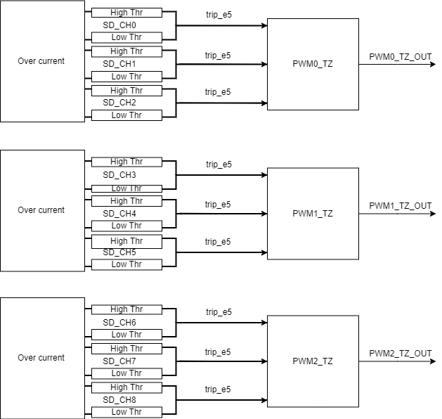
This section describes the over current implementation. It performs continuous sampling (free run) and when the sample value crosses the high or low threshold, the corresponding PWM trip status gets set and TZ_OUT pin goes high. It also stores high and low threshold status in DMEM for all channels, SDFM_getHighThresholdStatus API returns high threshold status for specified SDFM channel number and SDFM_getLowThresholdStatus API returns low threshold status for specified SDFM channel number.

This section describes the zero cross implementation. It compares the current sample and the previous sample values with zero cross threshold value.
There are two cases:


This section describes the EPWM to SDFM synchronization and trigger timing for each EPWM cycle. At the end of the every EPWM cycle, the EPWM generates a sync out event that resets the IEP timer. The firmware initiates normal current sampling at the sample trigger point in each EPWM cycle. It takes four consecutive samples to bring the accumulator and differentiator registers to stable state. It takes the first sample at the trigger point and the next three samples, each after ONE_SAMPLE_TIME. Here ONE_SAMPLE_TIME is: OSR*(1/SD_CLK)

The Fast Detect block is used for fast over current detection, it comparatively measures the number of zeros and ones presented in a programmable sliding window of 4 to 32 bits. It starts the comparison after the first 32 sample clocks. Based on the configured zero max/min count limits, it compares zero counter with these limits. If zero counter crosses limit then it sends a error signal to respective PWM Trip zone block. PWM TZ block receives this error signal and sets trip status bit to bring TZ_OUT pin output state to high.
Note: To identify the sigma delta fast detect error trip cause, SDFM_getFastDetectErrorStatus API can be used and to clear the PWM trip status, SDFM_clearPwmTripStatus API can be used.

Following points describe the process for measurement of phase difference between clock and data

| Pin name | Signal name | Function |
|---|---|---|
| GPIO_ZC_TH_CH0 | MCU_SPI0_D1/B6 | Ch0 High threshold output |
| GPIO_ZC_TH_CH1 | MCU_SPI1_CS0/A7 | Ch1 High threshold output |
| GPIO_ZC_TH_CH2 | MCU_SPI1_D1/C8 | Ch2 High threshold output |
| SD0_D | PIN_PRG0_PRU0_GPO1 | Channel0 data input |
| SD1_D | PIN_PRG0_PRU0_GPO3 | Channel1 data input |
| SD2_D | PIN_PRG0_PRU0_GPO5 | Channel2 data input |
| PRG0_ECAP0_IN_APWM_OUT | PIN_PRG0_PRU1_GPO15 | ECAP output frequency |
| GPIO_MTR_1_PWM_EN | GPMC0_AD15/Y20 | Enable EPWM0 on 3-axis board |
| SD8_CLK | PIN_PRG0_PRU0_GPO16 | Comman SDFM clock input pin |
| Pin name | Signal name | Function |
|---|---|---|
| GPIO_ZC_TH_CH0 | PRG1_PRU0_GPO18 | (J7.64)Ch0 Zero cross output |
| GPIO_ZC_TH_CH1 | PRG0_PRU1_GPO2 | (J7.65)Ch1 Zero cross output |
| GPIO_ZC_TH_CH2 | PRG0_PRU1_GPO1 | (J7.67)Ch2 Zero cross output |
| SD0_D | PIN_PRG0_PRU0_GPO1 | (J4.32)Channel0 data input |
| SD1_D | PIN_PRG0_PRU0_GPO3 | (J2.19)Channel1 data input |
| SD2_D | PIN_PRG0_PRU0_GPO5 | (J2.13)Channel2 data input |
| PRG0_ECAP0_IN_APWM_OUT | PIN_PRG0_PRU1_GPO15 | (J6.59)ECAP output frequency |
| SD8_CLK | PIN_PRG0_PRU0_GPO16 | (J1.7)Comman SDFM clock input pin |
| PWM0_TZ_OUT | PIN_PRG0_PRU0_GPO19 | (J5.45)TZ output pin for Axis-1 |
| PWM1_TZ_OUT | PIN_PRG0_PRU1_GPO19 | (J8.76)TZ output pin for Axis-2 |
| PWM2_TZ_OUT | PIN_PRG0_PRU1_GPO8 | (J6.57)TZ output pin for Axis-3 |
| PRG1_IEP0_EDC_SYNC_OUT0 | PIN_PRG1_PRU0_GPO19 | (J7.63) SYNC_OUT0 |
| PRG1_IEP0_EDC_SYNC_OUT1 | PIN_PRG1_PRU0_GPO17 | (J7.65) SYNC_OUT1 |
 1.8.20