Communication Protocol Spec
Abstract
The MSP430 Energy Measurement Design Center (EMDC) communication protocol is a communications specification for sending Energy Measurement specific data. It enables MSP430 equipped with Sigma Deltas (SD24) to design, debug, and communicate with tuning tools on host PCs. In addition to this function, it can also provide a mechanism for interfacing a Energy Measurement MCU to another host MCU or SoC in the context of a larger system. This document discusses the details of the protocol: packet types, packet structure, and transmission. It does not discuss implementations, either for target or host.
Commands Overview
This section will describe the commands exchanged between Energy Measurement Design Center and the target.
Commands from EMDC to Target
The following commands have API handlers on the target side:
- Configure Mode (0x01) - EMDC configures the application mode (IDLE, ACTIVE, CALIBRATION).
- Application Version (0x02) - EMDC reads device and firmware ID.
- Request Calibration Values (0x03) - EMDC requests the target to send all the calibration values. When the target is done it will send this command with the calibration request flag set to done.
- ADC Buffer Size (0x04) - EMDC reads the current and voltage buffer sizes to calculate the maximum and minimum preload allowed during calibration.
- Calibration Values (0xB0) - EMDC writes the calibration values to the working (RAM) calibration structure for Phase ID.
- Calibration Phase Configuration (0xB1) - EMDC configures the Phase ID being calibrated. After this command is received the target will send phase results. In CALIBRATION mode results will not be sent to the EMDC until this command is received. The Phase ID is cleared in the target when the application switches back to ACTIVE mode.
- Calibration Values Save (0xB2) - EMDC requests target to store calibration values for Phase ID in Flash. When the target is finished writing to Flash it will send this command with the Flash Write Flag set to true. Note The results commands do not have an API handler on the target. After EMDC configures the application mode to ACTIVE, then the target will send all the results for each phase to EMDC.
Commands from Target to EMDC
The following commands are handled by the EMDC HID interface:
- Application Version (0x02) - the target sends device and firmware ID after EMDC has sent this command in READ mode.
- Request Calibration Values (0x03) - the target sends calibration request flag after it finishes sending all the calibration values to EMDC. This allows the application to know when all the calibration values have been sent by the target.
- ADC Buffer Size (0x04) - the target sends the current and voltage buffer sizes.
- VRMS Result (0xB0) - the target sends the VRMS result (mV).
- IRMS Result (0xB1) - the target sends the IRMS result (uA).
- V Peak Result (0xB2) - the target sends the Voltage Peak result (mV).
- I Peak Result (0xB3) - the target sends the Current Peak result (uA).
- Power Factor Result (0xB4) - the target sends the Power Factor result.
- Frequency Result (0xB5) - the target sends the Frequency result (1x10⁻² Hz).
- Active Power Result (0xB6) - the target sends the Active Power result (uW).
- Reactive Power Result (0xB7) - the target sends the Reactive Power result (uVAr).
- Apparent Power Result (0xB8) - the target sends the Apparent Power result (uVA).
- Active Energy Result (0xB9) - the target sends the Active Energy result (uWh).
- Reactive Energy Result (0xBA) - the target sends the Reactive Energy result (uVArh).
- Apparent Energy Result (0xBB) - the target sends the Apparent Energy result (uVAh).
- Calibration Values (0xB0) - the target sends the calibration values stored in working (RAM) memory for Phase ID to EMDC.
- Calibration Values Save (0xB2) - the target sends the Flash Write Flag set to true after it finishes writing calibration values.
Protocol Overview
This section will explain how the protocol used between the EMDC and target using the commands previously explained using sequence diagrams.
The “Initial Commands Exchanged” figure shows the commands exchanged between EMDC and the target after the HID communication is established between EMDC and the hid bridge board. After these commands are sent the target will continue sending results for all the phases supported.
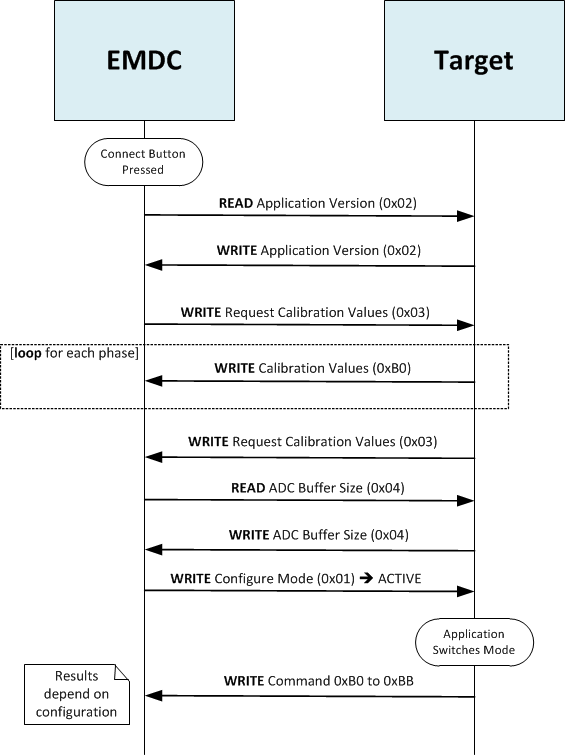
Fig. 128 Initial Commands Exchanged
The “Disconnect Commands Exchanged” figure shows the command sent from EMDC to the target at any time the Disconnect button is pressed on the GUI.
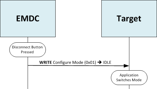
Fig. 129 Disconnect Commands Exchanged
The “Calibration Commands Exchanged” figure shows the commands exchanged between EMDC and the target when the user is initializing phase calibration mode on the GUI. Once the Calibration Phase Command is sent to the target, the target will continue sending results for the phase being calibrated. When the Apply Button is pressed the GUI will write the values to RAM and re-configure the SD24 (for phase calibration). The next set of results sent to EMDC will take into account the new calibration values. Once the phase has been calibrated and the user clicks the stop button, there will be an option to save the calibration results in Flash. If the user selects Yes, then the calibration values will be stored in Flash while all the global interrupts are disabled. Otherwise, the EMDC will configure the target in ACTIVE mode.
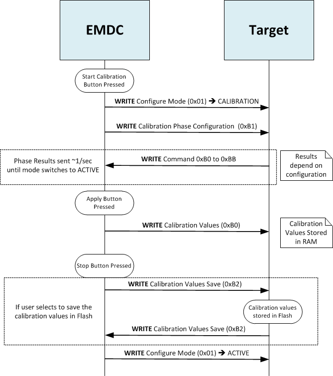
Fig. 130 Calibration Commands Exchanged
MSP430 EM Design Center Packet Structure
MSP EM Design Center generic Packet Structure | ||||||||||
|---|---|---|---|---|---|---|---|---|---|---|
[0] | [1] | [2] | [3] | [4] | [5] | [6] | ... | [N +1] | [N+2] | [N+3] |
MSP Design Center ID Byte | Command ID Byte | Read/Write Command Byte | Payload Byte0 | Payload Byte 1 | Payload Byte2 | Payload Byte3 | ... | Payload Byte N | Checksum (LSB) | Checksum (MSB) |
Byte Name | Byte Description |
MSP430 Design Center ID Byte | This byte identifies the package as a command for a specific Design Center GUI. In the case of MSP EM Design Center this byte is always 0x04. |
Command ID Byte | This byte specifies the command type. Each command has a fixed predefined lenght |
Read/Write Command Byte | This byte specifies is the command should be perform a read or write operation. 0x00 == Read 0x01 == Write |
Payload | Contains package payload |
Checksum | Checksum is a unsigned 16-bit value which contains the sum of Byte[0] - Byte[N+1] |
Configuration Parameters Description
All Result Parameter (Commands 0x01-0x04) contains 1-2 payload bytes. This section will describe the packet structure for each Configuration Parameter command.
Command 0x01 (Configure Mode)
Byte # | Description | Data Type | Valid Value/Range | Notes |
Byte 0 | Design Center ID | uint8_t | 0x04 | |
Byte 1 | Command | uint8_t | 0x01 | |
Byte 2 | Read/Write Command | uint8_t | 0x00 == Read 0x01 == Write | |
Byte 3 | Application Mode | uint8_t | 0x00 == IDLE 0x01 == ACTIVE 0x02 == CALIBRATION 0x03-0xff (Reserved) | IDLE = No results sent to EMDC ACTIVE = Results for all phases transmitted to EMDC CALIBRATION = Results from the phase being calibrated transmitted to EMDC |
Bytes [4-5] | Don’t care | N/A | N/A |
Command 0x02 (Application Version)
Byte # | Description | Data Type | Valid Value/Range | Notes |
Byte 0 | Design Center ID | uint8_t | 0x04 | |
Byte 1 | Command | uint8_t | 0x02 | |
Byte 2 | Read/Write Command | uint8_t | 0x00 == Read 0x01 == Write | |
Byte 3 | Device ID | uint8_t | 0x01 == MSP430i2021 0x03 == MSP430i2031 0x05 == MSP430i2041 0x25 == MSP430F6736 0x2B == MSP430F6736A 0x74 == MSP430F6779 0x79 == MSP430F6779A 0x84 == MSP430F67791 0x89 == MSP430F67791A | |
Byte 4 | Firmware ID | uint8_t | Firmware version | |
Bytes [5-6] | Don’t care | N/A | N/A |
Command 0x03 (Request Calibration Values)
Byte # | Description | Data Type | Valid Value/Range | Notes |
Byte 0 | Design Center ID | uint8_t | 0x04 | |
Byte 1 | Command | uint8_t | 0x03 | |
Byte 2 | Read/Write Command | uint8_t | 0x00 == Read 0x01 == Write | |
Byte 3 | Calibration Request Flag | uint8_t | 0x00 == Target has NOT received a request to send calibration values 0x01 == Target has received a request to send calibration values 0x02 == Target has transmitted all the phase calibration values to EMDC | |
Bytes [4-5] | Don’t care | N/A | N/A |
Command 0x04 (ADC Buffer Size)
Byte # | Description | Data Type | Valid Value/Range | Notes |
Byte 0 | Design Center ID | uint8_t | 0x04 | |
Byte 1 | Command | uint8_t | 0x04 | |
Byte 2 | Read/Write Command | uint8_t | 0x00 == Read 0x01 == Write | |
Byte 3 | Phase Voltage Array Size | uint8_t | Multiple of 2 | -1 x Size x OSR = minimum total preload used in calibration. |
Byte 4 | Phase Current Array Size | uint8_t | Multiple of 2 | Size x OSR = maximum total preload used in calibration |
Bytes [5-6] | Don’t care | N/A | N/A |
Result Parameters Description
All Result Parameter (Commands 0x80-0xAF) contains 5-9 payload bytes. This section will describe the packet structure for each Result Parameter command.
Command 0x80 (VRMS Result)
Byte # | Description | Data Type | Valid Value/Range | Notes |
Byte 0 | Design Center ID | uint8_t | 0x04 | |
Byte 1 | Command | uint8_t | 0x80 | |
Byte 2 | Read/Write Command | uint8_t | 0x00 == Read 0x01 == Write | |
Byte 3 | Phase ID | uint8_t | 0x01 == Phase A 0x02 == Phase B 0x04 == Phase C 0x08 == Phase D 0x10 == Phase E 0x20 == Phase F 0x40 == Neutral 0x80 == Total | |
Bytes [4-7] | RMS Voltage (mV) | uint32_t | 0x0000-0xFFFF FFFF | |
Bytes [8-9] | Don’t care | N/A | N/A |
Byte # | Description | Data Type | Valid Value/Range | Notes |
Byte 0 | Design Center ID | uint8_t | 0x04 | |
Byte 1 | Command | uint8_t | 0x81 | |
Byte 2 | Read/Write Command | uint8_t | 0x00 == Read 0x01 == Write | |
Byte 3 | Phase ID | uint8_t | 0x01 == Phase A 0x02 == Phase B 0x04 == Phase C 0x08 == Phase D 0x10 == Phase E 0x20 == Phase F 0x40 == Neutral 0x80 == Total | |
Bytes [4-7] | RMS Current (uA) | uint32_t | 0x0000-0xFFFF FFFF | |
Bytes [8-9] | Don’t care | N/A | N/A |
Command 0x82 (V Peak Result)
Byte # | Description | Data Type | Valid Value/Range | Notes |
Byte 0 | Design Center ID | uint8_t | 0x04 | |
Byte 1 | Command | uint8_t | 0x82 | |
Byte 2 | Read/Write Command | uint8_t | 0x00 == Read 0x01 == Write | |
Byte 3 | Phase ID | uint8_t | 0x01 == Phase A 0x02 == Phase B 0x04 == Phase C 0x08 == Phase D 0x10 == Phase E 0x20 == Phase F 0x40 == Neutral 0x80 == Total | |
Bytes [4-7] | Voltage Peak (mV) | uint32_t | 0x0000-0xFFFF FFFF | |
Bytes [8-9] | Don’t care | N/A | N/A |
Command 0x83 (I Peak Result)
Byte # | Description | Data Type | Valid Value/Range | Notes |
Byte 0 | Design Center ID | uint8_t | 0x04 | |
Byte 1 | Command | uint8_t | 0x83 | |
Byte 2 | Read/Write Command | uint8_t | 0x00 == Read 0x01 == Write | |
Byte 3 | Phase ID | uint8_t | 0x01 == Phase A 0x02 == Phase B 0x04 == Phase C 0x08 == Phase D 0x10 == Phase E 0x20 == Phase F 0x40 == Neutral 0x80 == Total | |
Bytes [4-7] | Peak Current (uA) | uint32_t | 0x0000-0xFFFF FFFF | |
Bytes [8-9] | Don’t care | N/A | N/A |
Byte # | Description | Data Type | Valid Value/Range | Notes |
Byte 0 | Design Center ID | uint8_t | 0x04 | |
Byte 1 | Command | uint8_t | 0x84 | |
Byte 2 | Read/Write Command | uint8_t | 0x00 == Read 0x01 == Write | |
Byte 3 | Phase ID | uint8_t | 0x01 == Phase A 0x02 == Phase B 0x04 == Phase C 0x08 == Phase D 0x10 == Phase E 0x20 == Phase F 0x40 == Neutral 0x80 == Total | |
Bytes [4-7] | Power Factor (ex 0.4251 = 4251) | uint32_t | 0x0000-0xFFFF FFFF | |
Bytes [8-9] | Don’t care | N/A | N/A |
Command 0x85 (Frequency Result)
Byte # | Description | Data Type | Valid Value/Range | Notes |
Byte 0 | Design Center ID | uint8_t | 0x04 | |
Byte 1 | Command | uint8_t | 0x85 | |
Byte 2 | Read/Write Command | uint8_t | 0x00 == Read 0x01 == Write | |
Byte 3 | Phase ID | uint8_t | 0x01 == Phase A 0x02 == Phase B 0x04 == Phase C 0x08 == Phase D 0x10 == Phase E 0x20 == Phase F 0x40 == Neutral 0x80 == Total | |
Bytes [4-5] | Phase frequency (1x10⁻² Hz) | uint16_t | 0x0000-0xFFFF | |
Bytes [6-7] | Don’t care | N/A | N/A |
Command 0x86 (Active Power Result)
Byte # | Description | Data Type | Valid Value/Range | Notes |
Byte 0 | Design Center ID | uint8_t | 0x04 | |
Byte 1 | Command | uint8_t | 0x86 | |
Byte 2 | Read/Write Command | uint8_t | 0x00 == Read 0x01 == Write | |
Byte 3 | Phase ID | uint8_t | 0x01 == Phase A 0x02 == Phase B 0x04 == Phase C 0x08 == Phase D 0x10 == Phase E 0x20 == Phase F 0x40 == Neutral 0x80 == Total | |
Bytes [4-11] | Active Power (uW) | int64_t | 0x0000-0xFFFF FFFF FFFF FFFF | |
Bytes [12-13] | Don’t care | N/A | N/A |
Command 0x87 (Reactive Power Result)
Byte # | Description | Data Type | Valid Value/Range | Notes |
Byte 0 | Design Center ID | uint8_t | 0x04 | |
Byte 1 | Command | uint8_t | 0x87 | |
Byte 2 | Read/Write Command | uint8_t | 0x00 == Read 0x01 == Write | |
Byte 3 | Phase ID | uint8_t | 0x01 == Phase A 0x02 == Phase B 0x04 == Phase C 0x08 == Phase D 0x10 == Phase E 0x20 == Phase F 0x40 == Neutral 0x80 == Total | |
Bytes [4-11] | Reactive Power (uVAr) | int64_t | 0x0000-0xFFFF FFFF FFFF FFFF | |
Bytes [12-13] | Don’t care | N/A | N/A |
Command 0x88 (Apparent Power Result)
Byte # | Description | Data Type | Valid Value/Range | Notes |
Byte 0 | Design Center ID | uint8_t | 0x04 | |
Byte 1 | Command | uint8_t | 0x88 | |
Byte 2 | Read/Write Command | uint8_t | 0x00 == Read 0x01 == Write | |
Byte 3 | Phase ID | uint8_t | 0x01 == Phase A 0x02 == Phase B 0x04 == Phase C 0x08 == Phase D 0x10 == Phase E 0x20 == Phase F 0x40 == Neutral 0x80 == Total | |
Bytes [4-11] | Apparent Power (uVA) | int64_t | 0x0000-0xFFFF FFFF FFFF FFFF | |
Bytes [12-13] | Don’t care | N/A | N/A |
Command 0x89 (Active Energy Result)
Byte # | Description | Data Type | Valid Value/Range | Notes |
Byte 0 | Design Center ID | uint8_t | 0x04 | |
Byte 1 | Command | uint8_t | 0x89 | |
Byte 2 | Read/Write Command | uint8_t | 0x00 == Read 0x01 == Write | |
Byte 3 | Phase ID | uint8_t | 0x01 == Phase A 0x02 == Phase B 0x04 == Phase C 0x08 == Phase D 0x10 == Phase E 0x20 == Phase F 0x40 == Neutral 0x80 == Total | |
Bytes [4-11] | Active Energy (uWh) | uint64_t | 0x0000-0xFFFF FFFF FFFF FFFF | |
Bytes [12-13] | Don’t care | N/A | N/A |
Command 0x8A (Reactive Energy Result)
Byte # | Description | Data Type | Valid Value/Range | Notes |
Byte 0 | Design Center ID | uint8_t | 0x04 | |
Byte 1 | Command | uint8_t | 0x8A | |
Byte 2 | Read/Write Command | uint8_t | 0x00 == Read 0x01 == Write | |
Byte 3 | Phase ID | uint8_t | 0x01 == Phase A 0x02 == Phase B 0x04 == Phase C 0x08 == Phase D 0x10 == Phase E 0x20 == Phase F 0x40 == Neutral 0x80 == Total | |
Bytes [4-11] | Reactive Energy (uVArh) | uint64_t | 0x0000-0xFFFF FFFF FFFF FFFF | |
Bytes [12-13] | Don’t care | N/A | N/A |
Command 0x8B (Apparent Energy Result)
Byte # | Description | Data Type | Valid Value/Range | Notes |
Byte 0 | Design Center ID | uint8_t | 0x04 | |
Byte 1 | Command | uint8_t | 0x8B | |
Byte 2 | Read/Write Command | uint8_t | 0x00 == Read 0x01 == Write | |
Byte 3 | Phase ID | uint8_t | 0x01 == Phase A 0x02 == Phase B 0x04 == Phase C 0x08 == Phase D 0x10 == Phase E 0x20 == Phase F 0x40 == Neutral 0x80 == Total | |
Bytes [4-11] | Apparent Energy (uVAh) | uint64_t | 0x0000-0xFFFF FFFF FFFF FFFF | |
Bytes [12-13] | Don’t care | N/A | N/A |
Calibration Parameters Description
All Calibration Parameter (Commands 0xB0-0xB2) contains 1-15 payload bytes. This section will describe the packet structure for each Configuration Parameter command.
Command 0xB0 (Calibration Values)
Byte # | Description | Data Type | Valid Value/Range | Notes |
Byte 0 | Design Center ID | uint8_t | 0x04 | |
Byte 1 | Command | uint8_t | 0xB0 | |
Byte 2 | Read/Write Command | uint8_t | 0x00 == Read 0x01 == Write | |
Byte 3 | Phase ID | uint8_t | 0x01 == Phase A 0x02 == Phase B 0x04 == Phase C 0x08 == Phase D 0x10 == Phase E 0x20 == Phase F 0x40 == Neutral | |
Bytes [4-7] | Voltage Scale Factor (IQ10) | int32_t | 0x0000-0xFFFF FFFF | |
Bytes [8-11] | Current Scale Factor (IQ26) | int32_t | 0x0000-0xFFFF FFFF | |
Bytes [12-15] | Active Power Scale Factor (IQ30) | int32_t | 0x0000-0xFFFF FFFF | |
Bytes [16-17] | Phase Correction Bit 0 - Bit 9 : Preload Bit 10 - Bit 15 : Whole Sample (signed) | int16_t | 0x0000-0xFFFF | |
Bytes [18-19] | Don’t care | N/A | N/A |
Command 0xB1 (Calibration Phase Configuration)
Byte # | Description | Data Type | Valid Value/Range | Notes |
Byte 0 | Design Center ID | uint8_t | 0x04 | |
Byte 1 | Command | uint8_t | 0xB1 | |
Byte 2 | Read/Write Command | uint8_t | 0x00 == Read 0x01 == Write | |
Byte 3 | Phase ID | uint8_t | 0x01 == Phase A 0x02 == Phase B 0x04 == Phase C 0x08 == Phase D 0x10 == Phase E 0x20 == Phase F 0x40 == Neutral | The results for this phase will be sent to the host in calibration mode. |
Bytes [4-5] | Don’t care | N/A | N/A |
Command 0xB2 (Calibration Values Save)
Byte # | Description | Data Type | Valid Value/Range | Notes |
Byte 0 | Design Center ID | uint8_t | 0x04 | |
Byte 1 | Command | uint8_t | 0xB2 | |
Byte 2 | Read/Write Command | uint8_t | 0x00 == Read 0x01 == Write | |
Byte 3 | Phase ID | uint8_t | 0x01 == Phase A 0x02 == Phase B 0x04 == Phase C 0x08 == Phase D 0x10 == Phase E 0x20 == Phase F 0x40 == Neutral | The calibration values for this phase will be saved to flash. | Byte 4 | Flash Write Flag | bool | true == Target finished writing calibration values to Flash. false == Target has NOT finished writing calibration values to Flash. |
Bytes [5-6] | Don’t care | N/A | N/A |
Document History
Version | Date | Author | Notes |
1.3 | April 12, 2018 | Erick Macias | Added diagrams describing communication sequence diagrams |
1.2 | April 6, 2018 | Erick Macias | Added calibration commands 0xB1, 0xB2 |
1.1 | April 30, 2018 | Erick Macias | Included all the result commands 0x80-0x8B |
1.0 | March 4, 2018 | Erick Macias | First draft of document |