The General-Purpose Memory Controller (GPMC) is an unified memory controller dedicated to interfacing external memory devices like
- Asynchronous SRAM like memories and application specific integrated circuit devices
- Asynchronous, synchronous, and page mode burst NOR flash devices
- NAND flash
- Pseudo-SRAM devices
System Configuration Overview
- Currently enabled for Memory Type: PSRAM (Pseudo Static Random Access Memory)
- Interface Width: 16 bits
- Memory Part Number: IS67WVE4M16EBLL-70BLA1
- Memory Capacity: 16Mb (8 MB)
Features Supported
- 16-bit wide data path to external memory device
- Supports up to 4 chip select regions of programmable size and programmable base addresses in a total address space of 1GB
- Fully pipelined operation for optimal memory bandwidth usage
- The clock to the external memory is provided from GPMC_FCLK divided by 1, 2, 3, or 4
- Supports programmable autoclock gating when no access is detected
- Independent and programmable control signal timing parameters for setup and hold time on a per-chip basis. Parameters are set according to the memory device timing parameters with a timing granularity of one GPMC_FCLK clock cycle.
- Flexible internal access time control (wait state) and flexible handshake mode using external WAIT pin monitoring
- Support bus keeping
- Support bus turnaround
- 32-bit interconnect target interface which supports non-wrapping and wrapping burst of up to 16x32 bits
SysConfig Features
- Note
- It is strongly recommend to use SysConfig where it is available instead of using direct SW API calls. This will help simplify the SW application and also catch common mistakes early in the development cycle.
- Set input clock frequency and clock divider
- Set interrupt trigger type
- Configuring pinmux based on selected pin
Features NOT Supported
- Interupt mode is not supported.
- Interface to NAND-like devices are not supported.
GPMC Overview
The GPMC basic programming model offers maximum flexibility to support various access protocols for each of the four configurable chip-selects. Use optimal chip-select settings, based on the characteristics of the external device:
- Different protocols can be selected to support generic asynchronous or synchronous random-access devices (NOR flash, SRAM) or to support specific NAND devices.
- The address and data bus can be multiplexed on the same external bus.
- Read and write access can be independently defined as asynchronous or synchronous.
- System requests (byte, 16-bit word, burst) are performed through single or multiple accesses. External access profiles (single, multiple with optimized burst length, native- or emulated-wrap) are based on external device characteristics (supported protocol, bus width, data buffer size, native-wrap support).
- System burst read or write requests are synchronous-burst (multiple-read or multiple-write). When neither burst nor page mode is supported by external memory or ASIC devices, system burst read or write requests are translated to successive single synchronous or asynchronous accesses (single reads or single writes). 8-bit wide devices are supported only in single synchronous or single asynchronous read or write mode.
- To simulate a programmable internal-wait-state, an external WAIT pin can be monitored to dynamically control external access at the beginning (initial access time) of and during a burst access. Each control signal is controlled independently for each chip-select. The internal functional clock of the GPMC (GPMC_FCLK) is used as a time reference to specify the following:
- Read- and write-access duration
- Most GPMC external interface control-signal assertion and deassertion times
- Data-capture time during read access
- External wait-pin monitoring time
- Duration of idle time between accesses, when required
Below figure shows the GPMC functional block diagram. The GPMC consists of six blocks:
- Interconnect port interface
- Address decoder, GPMC configuration, and chip-select configuration register file
- Access engine
- Prefetch and write-posting engine
- Error correction code engine (ECC)
- External device/memory port interface
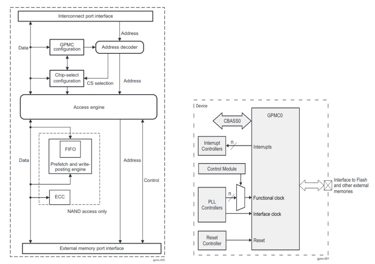
GPMC FUNCTIONAL BLOCK DIAGRAM
The GPMC can access various external devices. The flexible programming model allows a wide range of attached device types and access schemes. Based on the programmed configuration bit fields stored in the GPMC registers, the GPMC can generate the timing of all control signals depending on the attached device and access type. Given the chip-select decoding and its associated configuration registers, the GPMC selects the appropriate control signal timing for the device type
Example Usage
Include the below file to access the APIs
#include <stdio.h>
#include <drivers/gpmc.h>
GPMC Instance Open
GPMC Instance Close
API
APIs for GPMC


 1.8.20