|
CC13xx Driver Library
|
|
CC13xx Driver Library
|
Functions | |
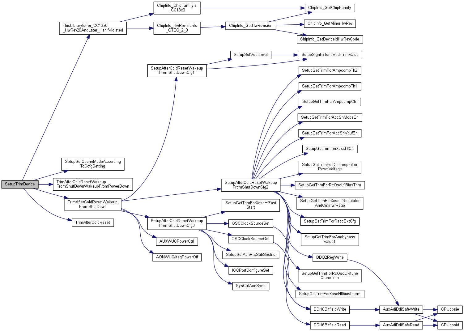
| void | SetupTrimDevice (void) |
| Performs the necessary trim of the device which is not done in boot code. More... | |
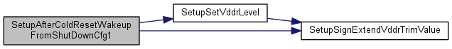
| void | SetupAfterColdResetWakeupFromShutDownCfg1 (uint32_t ccfg_ModeConfReg) |
| First part of configuration required when waking up from shutdown. More... | |
| void | SetupAfterColdResetWakeupFromShutDownCfg2 (uint32_t ui32Fcfg1Revision, uint32_t ccfg_ModeConfReg) |
| Second part of configuration required when waking up from shutdown. More... | |
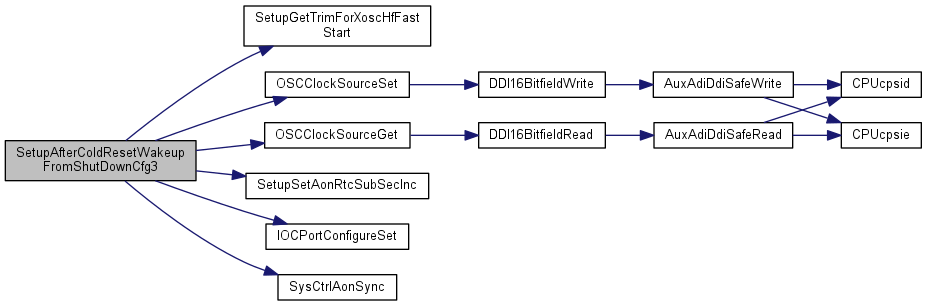
| void | SetupAfterColdResetWakeupFromShutDownCfg3 (uint32_t ccfg_ModeConfReg) |
| Third part of configuration required when waking up from shutdown. More... | |
| uint32_t | SetupGetTrimForAdcShModeEn (uint32_t ui32Fcfg1Revision) |
| Returns the trim value from FCFG1 to be used as ADC_SH_MODE_EN setting. More... | |
| uint32_t | SetupGetTrimForAdcShVbufEn (uint32_t ui32Fcfg1Revision) |
| Returns the trim value from FCFG1 to be used as ADC_SH_VBUF_EN setting. More... | |
| uint32_t | SetupGetTrimForAmpcompCtrl (uint32_t ui32Fcfg1Revision) |
| Returns the trim value to be used for the AMPCOMP_CTRL register in OSC_DIG. More... | |
| uint32_t | SetupGetTrimForAmpcompTh1 (void) |
| Returns the trim value to be used for the AMPCOMP_TH1 register in OSC_DIG. More... | |
| uint32_t | SetupGetTrimForAmpcompTh2 (void) |
| Returns the trim value to be used for the AMPCOMP_TH2 register in OSC_DIG. More... | |
| uint32_t | SetupGetTrimForAnabypassValue1 (uint32_t ccfg_ModeConfReg) |
| Returns the trim value to be used for the ANABYPASS_VALUE1 register in OSC_DIG. More... | |
| uint32_t | SetupGetTrimForDblrLoopFilterResetVoltage (uint32_t ui32Fcfg1Revision) |
| Returns the trim value from FCFG1 to be used as DBLR_LOOP_FILTER_RESET_VOLTAGE setting. More... | |
| uint32_t | SetupGetTrimForRadcExtCfg (uint32_t ui32Fcfg1Revision) |
| Returns the trim value to be used for the RADCEXTCFG register in OSC_DIG. More... | |
| uint32_t | SetupGetTrimForRcOscLfIBiasTrim (uint32_t ui32Fcfg1Revision) |
| Returns the FCFG1 OSC_CONF_ATESTLF_RCOSCLF_IBIAS_TRIM. More... | |
| uint32_t | SetupGetTrimForRcOscLfRtuneCtuneTrim (void) |
| Returns the trim value to be used for the RCOSCLF_RTUNE_TRIM and the RCOSCLF_CTUNE_TRIM bit fields in the XOSCLF_RCOSCLF_CTRL register in OSC_DIG. More... | |
| uint32_t | SetupGetTrimForXoscHfCtl (uint32_t ui32Fcfg1Revision) |
| Returns the trim value to be used for the XOSCHFCTL register in OSC_DIG. More... | |
| uint32_t | SetupGetTrimForXoscHfFastStart (void) |
| Returns the trim value to be used as OSC_DIG:CTL1.XOSC_HF_FAST_START. More... | |
| uint32_t | SetupGetTrimForXoscHfIbiastherm (void) |
| Returns the trim value to be used for the XOSC_HF_IBIASTHERM bit field in the ANABYPASS_VALUE2 register in OSC_DIG. More... | |
| uint32_t | SetupGetTrimForXoscLfRegulatorAndCmirrwrRatio (uint32_t ui32Fcfg1Revision) |
| Returns XOSCLF_REGULATOR_TRIM and XOSCLF_CMIRRWR_RATIO as one packet spanning bits [5:0] in the returned value. More... | |
| static int32_t | SetupSignExtendVddrTrimValue (uint32_t ui32VddrTrimVal) |
| Sign extend the VDDR_TRIM setting (special format ranging from -10 to +21) More... | |
| void | SetupSetCacheModeAccordingToCcfgSetting (void) |
| Set correct VIMS_MODE according to CCFG setting (CACHE or GPRAM) More... | |
| void | SetupSetAonRtcSubSecInc (uint32_t subSecInc) |
| Doing the tricky stuff needed to enter new RTCSUBSECINC value. More... | |
| void | SetupSetVddrLevel (uint32_t ccfg_ModeConfReg) |
| Set VDDR boost mode. More... | |
| void SetupAfterColdResetWakeupFromShutDownCfg1 | ( | uint32_t | ccfg_ModeConfReg | ) |
First part of configuration required when waking up from shutdown.
Referenced by TrimAfterColdResetWakeupFromShutDown().
| void SetupAfterColdResetWakeupFromShutDownCfg2 | ( | uint32_t | ui32Fcfg1Revision, |
| uint32_t | ccfg_ModeConfReg | ||
| ) |
Second part of configuration required when waking up from shutdown.
Referenced by TrimAfterColdResetWakeupFromShutDown().
| void SetupAfterColdResetWakeupFromShutDownCfg3 | ( | uint32_t | ccfg_ModeConfReg | ) |
Third part of configuration required when waking up from shutdown.
Referenced by TrimAfterColdResetWakeupFromShutDown().
| uint32_t SetupGetTrimForAdcShModeEn | ( | uint32_t | ui32Fcfg1Revision | ) |
Returns the trim value from FCFG1 to be used as ADC_SH_MODE_EN setting.
Referenced by SetupAfterColdResetWakeupFromShutDownCfg2().
| uint32_t SetupGetTrimForAdcShVbufEn | ( | uint32_t | ui32Fcfg1Revision | ) |
Returns the trim value from FCFG1 to be used as ADC_SH_VBUF_EN setting.
Referenced by SetupAfterColdResetWakeupFromShutDownCfg2().
| uint32_t SetupGetTrimForAmpcompCtrl | ( | uint32_t | ui32Fcfg1Revision | ) |
Returns the trim value to be used for the AMPCOMP_CTRL register in OSC_DIG.
Referenced by SetupAfterColdResetWakeupFromShutDownCfg2().
| uint32_t SetupGetTrimForAmpcompTh1 | ( | void | ) |
Returns the trim value to be used for the AMPCOMP_TH1 register in OSC_DIG.
Referenced by SetupAfterColdResetWakeupFromShutDownCfg2().
| uint32_t SetupGetTrimForAmpcompTh2 | ( | void | ) |
Returns the trim value to be used for the AMPCOMP_TH2 register in OSC_DIG.
Referenced by SetupAfterColdResetWakeupFromShutDownCfg2().
| uint32_t SetupGetTrimForAnabypassValue1 | ( | uint32_t | ccfg_ModeConfReg | ) |
Returns the trim value to be used for the ANABYPASS_VALUE1 register in OSC_DIG.
Referenced by SetupAfterColdResetWakeupFromShutDownCfg2().
| uint32_t SetupGetTrimForDblrLoopFilterResetVoltage | ( | uint32_t | ui32Fcfg1Revision | ) |
Returns the trim value from FCFG1 to be used as DBLR_LOOP_FILTER_RESET_VOLTAGE setting.
Referenced by SetupAfterColdResetWakeupFromShutDownCfg2().
| uint32_t SetupGetTrimForRadcExtCfg | ( | uint32_t | ui32Fcfg1Revision | ) |
Returns the trim value to be used for the RADCEXTCFG register in OSC_DIG.
Referenced by SetupAfterColdResetWakeupFromShutDownCfg2().
| uint32_t SetupGetTrimForRcOscLfIBiasTrim | ( | uint32_t | ui32Fcfg1Revision | ) |
Returns the FCFG1 OSC_CONF_ATESTLF_RCOSCLF_IBIAS_TRIM.
Referenced by SetupAfterColdResetWakeupFromShutDownCfg2().
| uint32_t SetupGetTrimForRcOscLfRtuneCtuneTrim | ( | void | ) |
Returns the trim value to be used for the RCOSCLF_RTUNE_TRIM and the RCOSCLF_CTUNE_TRIM bit fields in the XOSCLF_RCOSCLF_CTRL register in OSC_DIG.
Referenced by SetupAfterColdResetWakeupFromShutDownCfg2().
| uint32_t SetupGetTrimForXoscHfCtl | ( | uint32_t | ui32Fcfg1Revision | ) |
Returns the trim value to be used for the XOSCHFCTL register in OSC_DIG.
Referenced by SetupAfterColdResetWakeupFromShutDownCfg2().
| uint32_t SetupGetTrimForXoscHfFastStart | ( | void | ) |
Returns the trim value to be used as OSC_DIG:CTL1.XOSC_HF_FAST_START.
Referenced by SetupAfterColdResetWakeupFromShutDownCfg3().
| uint32_t SetupGetTrimForXoscHfIbiastherm | ( | void | ) |
Returns the trim value to be used for the XOSC_HF_IBIASTHERM bit field in the ANABYPASS_VALUE2 register in OSC_DIG.
Referenced by SetupAfterColdResetWakeupFromShutDownCfg2().
| uint32_t SetupGetTrimForXoscLfRegulatorAndCmirrwrRatio | ( | uint32_t | ui32Fcfg1Revision | ) |
Returns XOSCLF_REGULATOR_TRIM and XOSCLF_CMIRRWR_RATIO as one packet spanning bits [5:0] in the returned value.
Referenced by SetupAfterColdResetWakeupFromShutDownCfg2().
| void SetupSetAonRtcSubSecInc | ( | uint32_t | subSecInc | ) |
Doing the tricky stuff needed to enter new RTCSUBSECINC value.
Referenced by SetupAfterColdResetWakeupFromShutDownCfg3().
| void SetupSetCacheModeAccordingToCcfgSetting | ( | void | ) |
Set correct VIMS_MODE according to CCFG setting (CACHE or GPRAM)
Referenced by SetupTrimDevice().
| void SetupSetVddrLevel | ( | uint32_t | ccfg_ModeConfReg | ) |
Set VDDR boost mode.
Set VDDR boost mode.
Referenced by SetupAfterColdResetWakeupFromShutDownCfg1().

|
inlinestatic |
Sign extend the VDDR_TRIM setting (special format ranging from -10 to +21)
Referenced by SetupAfterColdResetWakeupFromShutDownCfg1(), SetupSetVddrLevel(), and SysCtrlSetRechargeBeforePowerDown().
| void SetupTrimDevice | ( | void | ) |
Performs the necessary trim of the device which is not done in boot code.
This function should only execute coming from ROM boot. The current implementation does not take soft reset into account. However, it does no damage to execute it again. It only consumes time.