LCD Controller
Description
Waveform generation for LCD, supporting any number of GPIO pins
This resource can generate complex waveforms at low update rate on any number of GPIO pins, typically for use with seven-segment LCDs (Liquid Crystal Displays) and similar. By using TI’s patented solution for driving LCDs, this can be done with regular digital GPIO pins connected to the LCD through an external resistor network.
Features:
- Can use any number of GPIO pins between DIO0 and DIO31 on the CC13x2/CC26x2 and CC13x4/CC26x4 devices
- Updates the waveform state (high, low or tri-state) for all used GPIO pins simultaneously, with one Sensor Controller instruction
- Designed for low-power operation at 2 MHz, but can also run fully or partially in active mode at 24 MHz if needed
- Typical waveform state update frequency between 300 Hz and 1 kHz
- The API for the System CPU application uses DIO pin mapping
- LCD image buffering scheme and mechanism for switching between LCD images are user-defined
This resource can only be used by one task per project. It is only supported by CC13x2/CC26x2 and CC13x4/CC26x4 devices.
The resource uses the dynamic I/O configuration in combination with the AUX Timer 2 event signals to update all I/O pins simultaneously. This means that the Timer 2 resource is not available when the LCD Controller resource is used.
Quick Introduction to LCD Operation
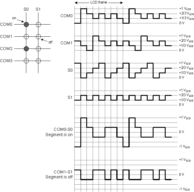
Each LCD segment is connected to a segment signal (Sn) and a common signal (COMn). With X segment signals and Y common signals, a total of X * Y LCD segments can be controlled.
To display a fixed image on the LCD, the LCD segments must be refreshed at a rate typically between 33 Hz and 100 Hz. This is done by repeating a sequence of 2 * Y waveform states, called an LCD frame.
In each LCD frame the common signals are “active” for one pair of waveform states each, the first state with normal signal polarity and the second state with inverse polarity. This, in combination with precise signal timing, ensures that the voltage over each LCD segment is DC-free. The LCD can be damaged over time if the voltage over each segment is not DC-free.
While the LCD is driven, the voltage over each segment is -1 VLCD, -1/3 VLCD, +1/3 VLCD or +1 VLCD.
- An LCD segment is ON if -1 VLCD and +1 VLCD are applied to the segment while its COM signal is active. -1/3 VLCD and +1/3 VLCD are applied to the segment while its COM signal is inactive.
- An LCD segment is OFF if only -1/3 VLCD and +1/3 VLCD are applied to the segment
To generate these COMn and Sn signal levels, TI’s patented LCD solution also requires one PWM signal and the inverse of that PWM signal. The COMn and Sn signals are generated through resistor networks as shown in the schematic below.
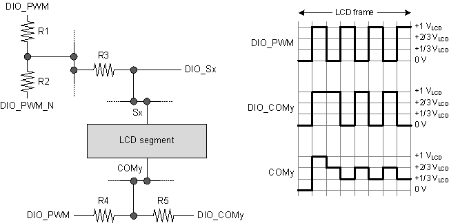
It is important to use as large resistor values as possible in order to minimize current consumption. The resistor values must be scaled according to the number of common and segment signals.
- R2 shall be 2 * R1. Typical values are R1 = 100 kOhm and R2 = 200 kOhm
- R3 shall be much higher than R2, so that the DIO_Sn signals have minimum effect on the shared PWM signal. Typical value is R3 = 10 MOhm.
- R4 shall be 2 * R5. Typical values are R4 = 2 MOhm and R5 = 1 MOhm
LCD Controller Implementation
The LCD controller is implemented partially by the Sensor Controller and partially by the System CPU application. The responsibilities are divided as follows:
- The System CPU application is responsible for preparing and loading the waveform states into the AUX RAM
- There must be one waveform state where all the GPIO pins are tri-stated, that is, the LCD display is not driven. This must be the initial state when starting the Sensor Controller task, and the final state when stopping the Sensor Controller task.
- The application must call
scifLcdInit()before the first call toscifLcdLoadState(). - The application must call
scifLcdLoadState()to load each LCD waveform state (output enable and output value for each DIO pin) into AUX RAM.
- The Sensor Controller is responsible for generating the LCD waveform with precise timing
- The waveform state sequencing must be implemented in task code. This allows for flexible sequencing that can include such as:
- Alternating between different LCD images, for scrolling effects, blinking effects, or alternating information
- Double-buffering when switching LCD image
- The Sensor Controller must call
lcdInit()when the LCD controller task is started - For each waveform state, the Sensor Controller must first call
lcdPrepareNextState()and thenlcdApplyNextState().lcdApplyNextState()must be called with precise timing, and is typically called immediately after Sensor Controller wake-uplcdPrepareNextState()does not need to be called with precise timing, and is typically called afterlcdApplyNextState(), to prepare for the next upcominglcdApplyNextState()call.- Note that this procedure takes considerable time to complete. See below for details.
- This procedure can be called in low-power mode, active mode, or during transition between these power modes
- The waveform state sequencing must be implemented in task code. This allows for flexible sequencing that can include such as:
Preparation Stage Timing
Since the lcdPrepareNextState() procedure takes considerable time to complete, it is useful to know more precisely how long it takes:
- Constant: Between 250 and 280 instructions, depending on variable placement in the AUX RAM*
- Variable: Between 15 and 17 instructions per pin, depending on variable placement in the AUX RAM*
- The timing does not depend on the pin states
* Low AUX RAM addresses can be accessed without a prefix instruction (first 1 kB or first 2 kB, depending on the instruction used).
Example: For 26 pins, the procedure uses 250 + (26 x 15) = 640 instructions.
Limitations
Be aware of the following limitations:
- The LCD contrast varies with the DIO supply voltages. This means that VDDS must be kept constant in order to maintain a fixed contrast. As stated in the CC13x2/CC26x2 and CC13x4/CC26x4 device data sheets (under Absolute Maximum Ratings), the DIO supply voltages cannot be set to different voltages than VDDS. This means that:
- The LCD contrast cannot be controlled dynamically without changing VDDS, which will affect other system functions
- If VDDS varies, for example as the battery voltage drops, the LCD contrast will change accordingly
- When debugging either Sensor Controller task code or the System CPU application, the Sensor Controller will be halted for longer periods of time. This will damage the LCD, due to DC voltage over the segments.
- Note that halting the System CPU will also halt the Sensor Controller, the RTC, and the 4 kHz signal used by Timer 0/1 event triggers
Examples
Initialization Code, Single Pattern
// Enable LCD waveform generation, position 0 = idle state (all LCD pins tri-stated)
lcdInit(0);

// Prepare the first waveform state update
state.patternPos = 1;
lcdPrepareNextState(state.patternPos);
Initialization Code, Alternating Patterns Triggered Autonomously
// Enable LCD waveform generation, position 0 = idle state (all LCD pins tri-stated)
lcdInit(0);

// Prepare the first waveform state update
state.patternStart = 1;
state.patternEnd = 8;
state.frameCounter = 1;
state.patternPos = state.patternStart;
lcdPrepareNextState(state.patternPos);
Event Handler Code, Single Pattern
// Apply the last prepared waveform state update
lcdApplyNextState();

// Find the next waveform state
if (state.patternPos == 8) {
    state.patternPos = 1;
} else {
    state.patternPos += 1;
}

// Prepare the next waveform state update
lcdPrepareNextState(state.patternPos);
Event Handler Code, Alternating Patterns Triggered Autonomously
// Apply the last prepared waveform state update
lcdApplyNextState();

// Find the next waveform state
state.patternPos += 1;
if (state.patternPos > state.patternEnd) {

    // New frame, so increment the frame counter, and switch LCD image at every 40 frames
    if (state.frameCounter == 40) {
        state.patternStart = 9;
        state.patternEnd   = 16;
        state.frameCounter = 41;
    } else if (state.frameCounter == 80) {
        state.patternStart = 1;
        state.patternEnd   = 8;
        state.frameCounter = 1;
    } else {
        state.frameCounter += 1;
    }
    state.patternPos = state.patternStart;
}

// Prepare the next waveform state update
lcdPrepareNextState(state.patternPos);
Termination Code
// Apply the last prepared waveform state update
lcdApplyNextState();

// Enter the idle state (tri-state all LCD pins)
lcdPrepareNextState(0);
lcdApplyNextState();
System CPU Application Code for Generating LCD Waveforms
// The following code shows how the desired LCD text is converted into a waveform that works with the
// Sensor Controller LCD resource. This code is not optimized, but is kept simple in order to show the
// principles.

// Waveform preparation buffer: Output enable and output value (one bit per DIO pin, one 32-bit word per
// waveform state)
uint32_t pWaveformDioEnable[8];
uint32_t pWaveformDioOutput[8];


// Segment I/O mapping look-up table: DIO pin = pSegPinToDioLut[LCD segment pin index]
const int pSegPinToDioLut[] = {
    16, 15, 14, 21, 20, 18, 7, 12, 10, 8, 6, 5, 4, 2, 1, 3, 9, 11, 13, 17, 19
};

// PWM and COM I/O mapping
#define DIO_PWM_N       27
#define DIO_PWM         26
#define DIO_COM3        25
#define DIO_COM2        24
#define DIO_COM1        23
#define DIO_COM0        22


// To enable an LCD segment, its segment signal is driven with opposite polarity of the PWM output
// while its common signal is active
void enableSeg(int segId) {
    int comPin = (segId - 1) % 4;
    int segPin = (segId - 1) / 4;
    pWaveformDioEnable[(2 * comPin) + 0] |= BV(pSegPinToDioLut[segPin]);
    pWaveformDioEnable[(2 * comPin) + 1] |= BV(pSegPinToDioLut[segPin]);
    pWaveformDioOutput[(2 * comPin) + 0] |= BV(pSegPinToDioLut[segPin]);
    pWaveformDioOutput[(2 * comPin) + 1] &= ~BV(pSegPinToDioLut[segPin]);
}


// To disable an LCD segment, its segment signal is driven by the PWM output while its common signal
// is active
void disableSeg(int segId) {
    int comPin = (segId - 1) % 4;
    int segPin = (segId - 1) / 4;
    pWaveformDioEnable[(2 * comPin) + 0] &= ~BV(pSegPinToDioLut[segPin]);
    pWaveformDioEnable[(2 * comPin) + 1] &= ~BV(pSegPinToDioLut[segPin]);
    pWaveformDioOutput[(2 * comPin) + 0] &= ~BV(pSegPinToDioLut[segPin]);
    pWaveformDioOutput[(2 * comPin) + 1] &= ~BV(pSegPinToDioLut[segPin]);
}


void clearDisplay(void) {
    for (int n = 0; n < 8; n++) {
        pWaveformDioEnable[n] = BV(DIO_PWM_N) | BV(DIO_PWM) | BV(DIO_COM3) | BV(DIO_COM2) | BV(DIO_COM1) | BV(DIO_COM0);
    }
    pWaveformDioOutput[0] = BV(DIO_PWM_N) | BV(DIO_COM3) | BV(DIO_COM2) | BV(DIO_COM1);
    pWaveformDioOutput[1] = BV(DIO_PWM)   | BV(DIO_COM0);
    pWaveformDioOutput[2] = BV(DIO_PWM_N) | BV(DIO_COM3) | BV(DIO_COM2) | BV(DIO_COM0);
    pWaveformDioOutput[3] = BV(DIO_PWM)   | BV(DIO_COM1);
    pWaveformDioOutput[4] = BV(DIO_PWM_N) | BV(DIO_COM3) | BV(DIO_COM1) | BV(DIO_COM0);
    pWaveformDioOutput[5] = BV(DIO_PWM)   | BV(DIO_COM2);
    pWaveformDioOutput[6] = BV(DIO_PWM_N) | BV(DIO_COM2) | BV(DIO_COM1) | BV(DIO_COM0);
    pWaveformDioOutput[7] = BV(DIO_PWM)   | BV(DIO_COM3);
}


// This function shows how to convert 7-segment characters              * 1 *
// into an LCD waveform, ready to be loaded into the Sensor             5   2
// Controller AUX RAM.                                                  * 6 *
//                                                                      7   3
// The LCD used here has 8 segments per character.                      * 8 *  4
void textToWaveform(char *pText) {
    clearDisplay();
    for (int n = 0; n < strlen(pText); n++) {
        switch (pText[n]) {
        case '0':
            enableSeg(1 + (n * 8));
            enableSeg(2 + (n * 8));
            enableSeg(3 + (n * 8));
            enableSeg(5 + (n * 8));
            enableSeg(7 + (n * 8));
            enableSeg(8 + (n * 8));
            break;
        case '1':
            enableSeg(2 + (n * 8));
            enableSeg(3 + (n * 8));
            break;
        case '2':
            enableSeg(1 + (n * 8));
            enableSeg(2 + (n * 8));
            enableSeg(6 + (n * 8));
            enableSeg(7 + (n * 8));
            enableSeg(8 + (n * 8));
            break;
        }
    }
}


void loadIdleState(int pos) {
    scifLcdLoadState(pos, 0x00000000, 0x00000000);
}


void loadWaveform(int basePos) {
    for (int n = 0; n < 8; n++) {
        scifLcdLoadState(n + basePos, pWaveformDioEnable[n], pWaveformDioOutput[n]);
    }
}


// Example of how to use the above functions: This loads two LCD images for the "Event Handler
// Code, Alternating Patterns Triggered Autonomously" example above.
void howToUseExample(void) {
    ... Initialize the Sensor Controller ...

    scifLcdInit();
    loadIdleState(0);
    textToWaveform(" 012    ");
    loadWaveform(1);
    textToWaveform("    210 ");
    loadWaveform(9);

    ... Start the LCD task ...
}
Procedures Overview
| Name | Brief description |
lcdApplyNextState() |
Applies the last prepared waveform state, by updating output enable and output value for LCD pins simultaneously, with one Sensor Controller instruction. More … |
lcdInit() |
Initializes the LCD controller resource. More … |
lcdPrepareNextState() |
Prepares the next waveform state update, by setting up output enable and output value for all LCD pins according to one of the states loaded by the scifLcdLoadState() SCIF driver function. More … |
Constants
| Name | Description |
LCD_STATE_COUNT |
Total number of LCD waveform states (idle, active and inactive) |
Global Variables
| Name | Description |
input.pLcdPattern00[] |
LCD pin patterns for AUXIO 03:00 |
input.pLcdPattern04[] |
LCD pin patterns for AUXIO 07:04 |
input.pLcdPattern08[] |
LCD pin patterns for AUXIO 11:08 |
input.pLcdPattern12[] |
LCD pin patterns for AUXIO 15:12 |
input.pLcdPattern16[] |
LCD pin patterns for AUXIO 19:16 |
input.pLcdPattern20[] |
LCD pin patterns for AUXIO 23:20 |
input.pLcdPattern24[] |
LCD pin patterns for AUXIO 27:24 |
input.pLcdPattern28[] |
LCD pin patterns for AUXIO 31:28 |
state.lcdCurrPatternPos |
The next pin pattern index |
state.lcdPrevPatternPos |
The previous pin pattern index |
Procedures
lcdApplyNextState
Prototype: lcdApplyNextState()
Applies the last prepared waveform state, by updating output enable and output value for LCD pins simultaneously, with one Sensor Controller instruction.
This procedure must be called exactly one time after each call to lcdPrepareNextState() .
This procedure must be called with precise timing.
lcdInit
Prototype: lcdInit(idlePatternPos)
Initializes the LCD controller resource.
This procedure must be called while all LCD pins are tri-stated, before the first call to lcdPrepareNextState() .
Parameter value(s)
- idlePatternPos : Initial LCD pattern position (all LCD pins tri-stated)
lcdPrepareNextState
Prototype: lcdPrepareNextState(nextPatternPos)
Prepares the next waveform state update, by setting up output enable and output value for all LCD pins according to one of the states loaded by the scifLcdLoadState() SCIF driver function.
This procedure must be called exactly one time before each call to lcdApplyNextState() .
This procedure does not need to be called with precise timing, and can be called in any power mode or during transitions between power modes. Note that the procedure takes significant time to complete, approximately 250 instructions base overhead + approximately 15 instructions per pin.
Parameter value(s)
- nextPatternPos : Next LCD waveform pattern position (takes effect on the next lcdApplyNextState() call).