|
MCUSW
|
|
MCUSW
|
This document describes the functionality, API and configuration of the AUTOSAR BSW module PWM
The figure below depicts the AUTOSAR layered architecture as 3 distinct layers,
The BSW is further divided into 4 layers:

MCAL is the lowest abstraction layer of the Basic Software. It contains software modules that interact with the Microcontroller and its internal peripherals directly. The PWM driver is a part of the microcontroller (peripheral) Driver module which is a part of the Basic Software. The figure below shows the position of the PWM driver in the AUTOSAR Architecture.

The PWM module implements an interface in C programming language for handling the PWM functionality of the device.This PWM driver takes care of initializing and de-initializing the PWM unit and offers services to:

In this design, the PWM Functionality can be achieved by using either of two available IPs, the DM Timers, or EPWM module.
DM Timer available on the device are used. TDA4x class of devices includes multiple timers, some of the key features provided are listed below:
There is Support for 3 basic functional modes Timer mode, Capture mode & Compare mode. Refer section 12.8.3 in 2 for more details on timer operation.
Timer pins can be configured to be used as PWM output pins. However, not all timer pins can be configured to be PWM output, please refer TRM for specific pins (section 12.8.3.1 in 2)
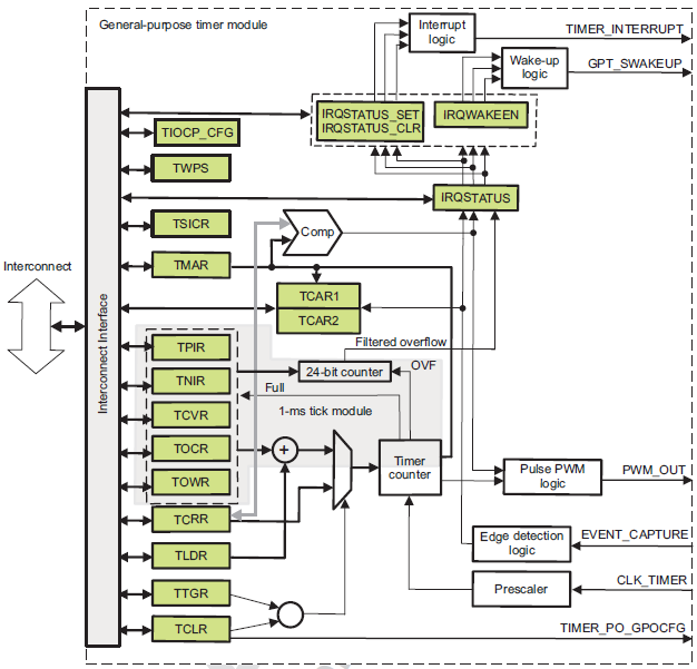
The following image shows the block diagram of Timer which can generate a PWM output:
The ePWM(enhanced) unit described here addresses these requirements by allocating all needed timing and control resources on a per PWM channel basis. Cross coupling or sharing of resources has been avoided; instead, the ePWM is built up from smaller single channel modules with separate resources and that can operate together as required to form a system. This modular approach results in easy understand of its operation quickly.
J7 family device include six instances of ePWM. The EPWM module represents one complete PWM channel composed of two PWM outputs: EPWMxA and EPWMxB. A given EPWM module functionality can be extended with the so called High-Resolution Pulse Width modulator.
In the further description the letter x within a signal or module name is used to indicate a generic EPWM instance on a device. For example, output signals EPWMxA and EPWMxB refer to the output signals from the EPWMx instance.
There are 6 instances of the EPWM integrated in the device. Each of the Enhanced Pulse Width Modulator (EPWM) includes an Enhanced High Resolution Modulator (HRPWM). The high-resolution functionality is implemented only on the EPWMxA output. EPWMxB output has conventional PWM capabilities. At system level the EPWM0 through EPWM5 integration features are listed below:
The high-resolution pulse-width modulator (HRPWM) extends the time resolution capabilities of the conventionally derived digital pulse-width modulator (PWM). HRPWM is typically used when PWM resolution falls below ~9-10 bits. The key features of HRPWM are:
")
| Sl No | Specification | Comment / Link |
|---|---|---|
| 1 | AUTOSAR 4.3.1 | AUTOSAR Specification for PWM Driver Intranet Link |
| 2 | TDA4x TRM | Technical Reference Manual, TDA4X PWM/DM Timer Module is detailed |
| 3 | BSW General Requirements / Coding guidelines | Intranet Link |
| 4 | Software Product Specification (SPS) | Intranet Link Requirements are derived from 1 |
The PWM driver shall implement as per requirements detailed in 4, 1 and 3. It is recommended to refer 1 for clarification.
Below listed are some of the key features that are expected to be supported
| Design ID | DES_PWM_001 |
| Requirements Covered | MCAL-965, MCAL-3503, MCAL-3509, MCAL-3511, MCAL-3536, MCAL-3537, MCAL-3538, MCAL-3539, MCAL-3540, MCAL-3554, MCAL-3510, MCAL-3631, MCAL-3535, MCAL-920, MCAL-921, MCAL-922, MCAL-923, MCAL-925,MCAL-929, MCAL-930, MCAL-932, MCAL-933, MCAL-937, MCAL-938, MCAL-939,MCAL-942, MCAL-947, MCAL-980, MCAL-945, MCAL-1056 , MCAL-3502, MCAL-3503, MCAL-3509, MCAL-3511, MCAL-3535, MCAL-3631, MCAL-4475 |

| Design ID | DES_PWM_002 |
| Non Requirements | MCAL-3648,MCAL-3642,MCAL-3493,MCAL-3482,MCAL-3522,MCAL-3532,MCAL-3531, MCAL-3512,MCAL-3614,MCAL-3481,MCAL-3613,MCAL-3515,MCAL-3626,MCAL-3478, MCAL-3513,MCAL-3628,MCAL-3629,MCAL-3606,MCAL-3617,MCAL-3602,MCAL-3516, MCAL-3638,MCAL-3608,MCAL-3619,MCAL-3609,MCAL-3514,MCAL-3518,MCAL-3519, MCAL-3630,MCAL-3543,MCAL-3604,MCAL-3517,MCAL-3544,MCAL-3610,MCAL-3627, MCAL-3618,MCAL-3605,MCAL-3639,MCAL-3620,MCAL-3603,MCAL-3521,MCAL-3621, MCAL-3607,MCAL-3484,MCAL-3615,MCAL-3483,MCAL-3622,MCAL-3611,MCAL-3530, MCAL-3520,MCAL-3601,MCAL-3612,MCAL-3623,MCAL-3529,MCAL-3616,MCAL-3489, MCAL-3588,MCAL-3589,MCAL-3591,MCAL-3590,MCAL-3497 |
Below listed are assumed to valid for this design/implementation, exceptions and other deviations are listed for each explicitly. Care should be taken to ensure these assumptions are addressed.
Some of the critical constraints of this design are listed below
| Design ID | DES_PWM_003 |
| Requirements Covered | MCAL-3493, MCAL-3502 |
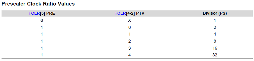
Setting Prescalers: Period value(Num of ticks) which determines the period is calculated using below formula:
Actual Division Value = / ( 1 << CLKDIV) i.e
| Actual Division Value | CLKDIV Value |
|---|---|
| 0x0 | / 1 |
| 0x1 | / 2 |
| 0x2 | / 4 |
| 0x3 | / 8 |
| 0x4 | / 16 |
| 0x5 | / 32 |
| 0x6 | / 64 |
| 0x7 | / 128 |
Actual Division Value = / (HSPCLKDIV * 2) i.e
| Actual Division Value | HSPCLKDIV |
|---|---|
| 0x0 | / 1 |
| 0x1 | / 2 |
| 0x2 | / 4 |
| 0x3 | / 6 |
| 0x4 | / 8 |
| 0x5 | / 10 |
| 0x6 | / 12 |
| 0x7 | / 14 |
There is a chance that period value calculated is fractional, and therefore required frequency cannot be achieved. The clock dividers need to be selected correctly to avoid such errors. Please refer to the excel sheet provided to derive the correct CLKDIV and HSPCLKDIV values. Using this excel, you can test prescaler combinations with required frequency and ensure that the "Difference" is 0. The Period value should be less than or equal to 65535 (16bit HW register size for period).
Find the excel sheet here: Period Calculator
The timer can be configured to provide a programmable PWM output. The timer PWM (POTIMERPWM) output pin can be configured to toggle on an event. The TCLR[11-10] TRG bit field determines on which register value the PWM pin toggles. Either overflow or both overflow and match can be selected to toggle the timer PWM pin when a compare condition occurs. TMAR, TLDR The internal overflow pulse is set each time the (0xFFFF FFFF – TLDR[31-0] LOAD_VALUE + 1) value is reached, and the internal match pulse is set when the counter reaches the value of TMAR. Depending on the value of the TCLR[12] PT bit and TCLR[11-10] TRG bit field, the timer provides pulse or PWM event on the output pin (POTIMERPWM). The TLDR and TMAR must keep values below the overflow value (0xFFFF FFFF) by at least two units. If the PWM trigger events are both overflow and match, the difference between the values kept in the TMAR and the value in the TLDR must be at least two units. When match event is used, the compare mode TCLR[6] CE bit must be set.
The following sequence of steps needs to be performed, before the timer can be started

For generating a PWM signal from the timer interrupts, the following cases w.r.t. duty cycle are considered:
Case 1: Duty cycle of 0%
CASE 2: Duty cycle of 100%
Case 3: Duty cycle of 50%
When the When a duty cycle of 50% for a PWM signal is required, both the time that the pulse remains HIGH and LOW is equal. In this case, the timer is operated in overflow mode alone (without compare). In one cycle of the PWM signal, the timer should generate an interrupt twice. Hence, the overflow rate for the timer (OVF_Rate) is half the period of the PWM signal required. The load value for TLDR register can be calculated using the following formula:
OVF_Rate = (0xFFFF FFFF – TLDR + 1) × (timer-functional clock period) × PS
where
Case 4: 0%< Duty cycle < 100%
When PWM signal with 0%< duty cycle < 100% for a is required, the timer is operated in overflow and match mode (with compare). In one cycle of the PWM signal, the timer generates an interrupt twice, one when the match condition is met and one when overflow is triggered as shown in the figure below.Hence, in this scenario, the overflow rate for the timer (OVF_Rate) is same as the period of the PWM signal required.

The load value for TLDR and TMAR registers can be calculated using the following formula:
OVF_Rate = (0xFFFF FFFF – TLDR + 1) × (timer-functional clock period) × PS
OVF_Rate * (1- (Dutycyle/100)) = (0xFFFF FFFF – TMAR + 1) × (timer-functional clock period) × PS
where
Two example cases are shown in the following figure. The TCLR[7] SCPWM bit is set to 0 in one case and to 1 in the other case. To obtain the desired wave form, start the counter at 0xFFFF FFFE value (to ensure an overflow first) or adjust the line polarity (TCLR[7] SCPWM bit).

NOTE

EPWM Module in J721E/J7200 consist of submodules:
Time-base (TB)
Counter-compare (CC)
Action-qualifier (AQ)
Event-trigger (ET)
High-Resolution PWM (HRPWM)


As the PWM module is implemeted using a timer, as detailed in section 7.1 of 5, a timer would be in one of the following states. Initialized, running, stopped, expired. The diagram below shows transitions of states:

Refer 1 specifically section 7.2 of the specification for more details All time units used within the API services of the PWM module shall be of the unit ticks.
| Design ID | DES_PWM_004 |
| Requirements Covered | MCAL-3511 |
Refer 1 specifically section 7.7 of the specification for more details The width of the duty cycle parameter is 16 Bits and the parameter follows the following scaling scheme:
As an implementation guide, the following source code example is given:
AbsoluteDutyCycle =((uint32)AbsolutePeriodTime * RelativeDutyCycle) >> 15;
| Design ID | DES_PWM_005 |
| Requirements Covered | MCAL-3533,MCAL-3534 |
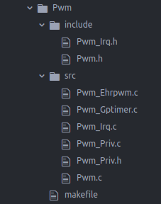
The directory structure is as depicted in figures below, the source files can be categorized under “Driver Implementation” and “Example Application”
Driver Implemented by

| Design ID | DES_PWM_006 |
| Requirements Covered | MCAL-3503,MCAL-3507,MCAL-3506,MCAL-3504,MCAL-3508,MCAL-3505 |
The AUTOSAR PWM Driver Specification details mandatory parameters that shall be configurable via the configurator. Please refer section 10 of 1
| Design ID | DES_PWM_007 |
| Requirements Covered | MCAL-3474,MCAL-3475,MCAL-3476,MCAL-3477,MCAL-3478,MCAL-3479,MCAL-3480, MCAL-3481,MCAL-3482,MCAL-3483,MCAL-3484,MCAL-3485,MCAL-3486,MCAL-3487, MCAL-3488,MCAL-3489,MCAL-3490,MCAL-3491,MCAL-3492,MCAL-3493,MCAL-3494, MCAL-3495,MCAL-3496,MCAL-3497,MCAL-3498,MCAL-3499,MCAL-3500,MCAL-3501, MCAL-3652, MCAL-4479 |
The design's specific configurable parameters are as follows:
| Parameter | Usage comment |
|---|---|
| PwmDeviceVariant | This shall allow integrators to select the device variant for which integration is being performed. This parameter shall be used by driver to impose device specific constraints. The user guide shall detail the device specific constraints |
| PwmFunctionalClock | This is the value of the System clock frequency in Hz |
| PwmTypeofInterruptFunction | This parameter allows the selection of Type of ISR function |
| PwmEnableRegisterReadbackApi | This parameter enables the API to readback PWM critical registers |
| PwmClkPrescaler | This parameter allows the selection of pre-scalar value.The prescaler stage is clocked with the pwm clock and acts as a clock divider for the time-base clock. |
| PwmPolarity | This parameter stores the initial polarity configured for a channel |
| PwmIdleState | This parameter stores whether the channel is in idle state |
| PwmDefaultOSCounterId | This parameter stores Default Os Counter Id if node reference to OsCounter ref PwmOsCounterRef is not set |
| PwmOsCounterRef | This parameter contains a reference to the OsCounter, which is used by the Timer driver |
| PwmTimeoutDuration | This parameter contains the Timer timeout upper limit |
| Design ID | DES_PWM_008 |
| Requirements Covered | MCAL-3653, MCAL-3654, MCAL-3660, MCAL-3657, MCAL-3752 ,MCAL-3753, MCAL-3754, MCAL-3655 |
| Parameter | Usage comment |
|---|---|
| PwmOutputChSelect | PWM Output Channel select EPWMxA or EPWMxB or Both. Both Outputs available with same duty cycle, period and polarity. |
| PwmHSClkPrescaler | This parameter allows the selection of High Speed pre-scalar value. The High Speed prescaler stage is clocked with the pwm clock and acts as a clock divider for the time-base clock. High-Speed Time-base Clock Prescale Bits. |
| PwmEnableHighRes | This parameter will be a switch to enable or disable high resolution (HRPWM) capability of EPWM module. |
Standard Config which will be used to differentiate between Gptimer and EHRPWM mode of operation.
| Parameter | Usage comment |
|---|---|
| PwmIndex | Specifies the InstanceId of this module instance. |
Output Channel Structure:
The driver shall support both VARIANT-POST-BUILD & VARIANT-PRE-COMPILE
| Design ID | DES_PWM_009 |
| Requirements Covered | MCAL-3647, MCAL-3647 |
In addition to dependencies listed in section 5 of 1, PWM driver shall depend on these modules to realize the required functionality. PWM uses Timer hardware present in the device to realize the functionality, this peripheral requires 2 different clock to be operational, namely ICLK and FCLK.
Errors are classified in two categories, development error and runtime / production error.
| Type of Error | Related Error code | Value (Hex) | Refer Req |
| API Pwm_Init service called with wrong parameter | PWM_E_PARAM_CONFIG | 0x10 | MCAL-3523 |
| API service used without module initialization | PWM_E_UNINIT | 0x11 | MCAL-3524 |
| API service used with an invalid channel Identifier | PWM_E_PARAM_CHANNEL | 0x12 | MCAL-3525 |
| Usage of unauthorized PWM service on PWM channel configured a fixed period | PWM_E_PERIOD_UNCHANGEABLE | 0x13 | MCAL-3526 |
| API Pwm_Init service called while the PWM driver has already been initialised | PWM_E_ALREADY_INITIALIZED | 0x14 | MCAL-3527 |
| API Pwm_GetVersionInfo is called with a NULL parameter. | PWM_E_PARAM_POINTER | 0x15 | MCAL-3528 |
| Design ID | DES_PWM_010 |
| Requirements Covered | MCAL-3523, MCAL-3524, MCAL-3525, MCAL-3526, MCAL-3527, MCAL-3528, MCAL-4480, MCAL-4481 |
The detection of development errors is configurable (ON / OFF) at pre-compile time. The switch PwmDevErrorDetect will activate or deactivate the detection of all development errors.
All detected development errors are reported to Det_ReportError service of the Development Error Tracer (DET).
| Design ID | DES_PWM_011 |
| Requirements Covered | MCAL-3649 |
| Design ID | DES_PWM_012 |
| Requirements Covered | MCAL-3650 |
This PWM design is based on the requirements specification for AUTOSAR versioned 4.2.1 and sections below highlight some of the critical changes that would be required between these two versions.
Note that this design doesn’t comprehend or account for other versions of AUTOSAR.
Probably easiest of all to implement. The following have been removed from the requirements specification for AUTOSAR versioned 4.4.0:
The following changes have been added in the configurator in the requirements specification for AUTOSAR versioned 4.4.0
The following changes have been added in the requirements specification for AUTOSAR versioned 4.4.0 :
The detailed API and interface description is available as part of 1 & 4. This section describes the API supported by the MCAL driver and the requirements covered by each of the API.
The sections below lists some of key data structures that shall be implemented and used in driver implementation
| Type | Identifier | Comments |
|---|---|---|
| uint32 | PWM_MAX_CHANNELS | Defines the maximum number of channels that are configured. Its required that configurations for all channel specified is valid. |
Used to specify the numeric identifier for a channel, please refer section 8.2.1 of 1
Used to specify the period of a PWM channel, refer section 8.2.2 of 1
Used to specify the Output state of a PWM channel, refer section 8.2.3 of 1
Enumeration used to specify the type of edge notification of a PWM channel. Refer section 8.2.4 of 1
Enumeration used to specify the class of a PWM channel, whether the period is fixed or not. Refer section 8.2.5 of 1
Hardware dependent structure used to specify the initial data for the PWM driver. Refer section 8.2.6 of 1
| Name | IP | Type | Range | Comments |
|---|---|---|---|---|
| pwmRev | GPT | uint32 | 0 to 0xFFFFFFFF | H/W version identifier, will not change for a given SoC |
| pwmTtgr | GPT | uint32 | 0 to 0xFFFFFFFF | Shall always read 0xFFFFFFFF |
| pwmTimerSynCtrl | GPT | uint32 | 0 to 0xFFFFFFFF | Interface control register, will read 0x00000000 |
| pwmTbCtl | EPWM | uint16 | 0 to 0xFFFF | Time base Control register |
| pwmTbPhs | EPWM | uint16 | 0 to 0xFFFF | Time base Counter Phase register |
| pwmTbCnt | EPWM | uint16 | 0 to 0xFFFF | Time base Counter Register |
| Design ID | DES_PWM_013 |
| Requirements Covered | MCAL-3536, MCAL-3537 ,MCAL-3538, MCAL-3539, MCAL-3540, MCAL-3541, MCAL-3542,MCAL-3662 |
For the standard APIs please refer 8.3 of 1. Sections below highlight other design considerations for the implementation.
Refer section 8.3.1 of 1
| Design ID | DES_PWM_014 |
| Requirements Covered | MCAL-3553, MCAL-3554, MCAL-3555, MCAL-3558, MCAL-3545, MCAL-3546, MCAL-3547, MCAL-3548, MCAL-3551, MCAL-3552, MCAL-3556, MCAL-3549,MCAL-3550 |
Refer section 8.3.2 of 1
| Design ID | DES_PWM_015 |
| Requirements Covered | MCAL-3560, MCAL-3559, MCAL-3561,MCAL-3562,MCAL-3563, MCAL-3564,MCAL-3643, MCAL-3640, MCAL-3641, MCAL-3642 |
Refer section 8.3.3 of 1
| Design ID | DES_PWM_016 |
| Requirements Covered | MCAL-3565,MCAL-3566, MCAL-3567,MCAL-3568,MCAL-3569, MCAL-3533,MCAL-3534,MCAL-3570,MCAL-3643, MCAL-3645, MCAL-3640, MCAL-3641,MCAL-3642,MCAL-3571,MCAL-3572 |
Refer section 8.3.4 of 1
| Design ID | DES_PWM_017 |
| Requirements Covered | MCAL-3573,MCAL-3574,MCAL-3575, MCAL-3576,MCAL-3533 ,MCAL-3534,MCAL-3643, MCAL-3644, MCAL-3645, MCAL-3640, MCAL-3641, MCAL-3642,MCAL-3577,MCAL-3578,MCAL-3579, MCAL-3580 |
Refer section 8.3.5 of 1
| Design ID | DES_PWM_018 |
| Requirements Covered | MCAL-3581, MCAL-3582, MCAL-3583, MCAL-3584, MCAL-3585 MCAL-3586,MCAL-3587 |
Refer section 8.3.7 of 1
| Design ID | DES_PWM_019 |
| Requirements Covered | MCAL-3592,MCAL-3593,MCAL-3594,MCAL-3595, MCAL-3643, MCAL-3645, MCAL-3640, MCAL-3641, MCAL-3642 |
Refer section 8.3.8 of 1
| Design ID | DES_PWM_020 |
| Requirements Covered | MCAL-3596, MCAL-3597,MCAL-3598, MCAL-3599,MCAL-3600, MCAL-3643, MCAL-3645, MCAL-3640, MCAL-3641, MCAL-3642 |
Refer section 8.3.13 of 1
| Design ID | DES_PWM_021 |
| Requirements Covered | MCAL-3624 |
As noted from previous implementation, the timer configuration registers could potentially be corrupted by other entities (s/w or h/w). One of the recommended detection methods would be to periodically read-back the configuration and confirm configuration is consistent. The service API defined below shall be implemented to enable this detection.
| Description | Comments | |
| Service Name | Pwm_RegisterReadback | Can potentially be turned OFF |
| Syntax | Std_ReturnType Pwm_RegisterReadback(Pwm_ChannelType PwmChannel, Pwm_RegisterReadbackType * RegRbPtr) | Pwm_RegisterReadbackType defines the type, that holds critical values, refer below |
| Service ID | 0x0F | |
| Sync / Async | Sync | |
| Reentrancy | Non Reentrant | |
| Parameter in | PwmChannel | Identifies a unique valid channel |
| Parameters out | RegRbPtr | A pointer of type Pwm_RegisterReadbackType, which holds the read back values |
| Return Value | Standard return type | E_OK or E_NOT_OK in case of invalid channel id |
The critical register listed is a recommendation and implementation shall determine appropriate registers.
This service could potentially be turned OFF in the configurator.
| Design ID | DES_PWM_022 |
| Requirements Covered | MCAL-3662,MCAL-3656 |
This design expects that implementation will require to use following global variables.
| Variable | Type | Description | Default Value |
|---|---|---|---|
| Pwm_DrvStatus | uint8 | PWM driver status | PWM_STATUS_UNINIT |
| Pwm_ChObj | Pwm_ChObjType | PWM channel object | - |
The following tests can be applied as diagnostics for this module (to provide diagnostic coverage on a specific function):
The following tests can be applied as diagnostics for this module (to provide diagnostic coverage on a specific function):
Section below list some of the important design decisions and rational behind those decisions.
The PWM signal generation when duty cycle is 50% and 0% < duty cycle < 100% can be done in the following ways:
The PWM signal generation from the timer should be optimized.
The PWM module is more efficeintly implemented by operating timer in overflow mode alone when duty cycle of 50% is required as this avoids the continuous register compare to TMAR to generate the trigger at compare condition. The configuration to overflow or overflow and compare in different duty cycles needs to be done one time, and is a lesser overhead.
| Design ID | DES_PWM_023 |
| Requirements Covered | MCAL-3533,MCAL-3534 |
The PWM module instance can use either Gptimer hardware or the EPWM hardware IP as the source for signal creation. The most efficient way of integrating both IP into PWM module has to be analyzed.
The PWM driver implementation and interface should be simple and user friendly. The user should be able to choose which one to use.
Option 1 is chosen as it is most compatible with the configurator and also will make the integration simpler. As mentioned above, the PwmIndex (PWM_INSTANCE_ID) variable will be used as the configuration parameter to choose between EPWM(default) or Gptimer. PWM_Priv.c will call the respective API (will be differentiated using the PWM_INSTNACE_ID).
HRPWM is based on micro edge positioner (MEP) technology. MEP logic is capable of positioning an edge finely by sub-diving one coarse system clock of a conventional PWM generator.
The PWM driver implementation should avoid any failure risks.
Option 1 is chosen. Typically MEP scale factor is calibrated in hardware. However, the current hardware does not have an in-built calibration/diagnostic module, so different MEP values cannot be analyzed at run-time. Keeping a fixed MEP value which is suggested by datasheet (180ps) would make the driver functionality simple and stable.
The PWM module instance is composed of two PWM outputs: EPWMxA and EPWMxB. It is possible to consider each output as one channel. In this way we can support 12 PWM outputs in case of J721E/J7200 simultaneously.
The PWM driver implementation and interface should be easily controllable.
Typically in PWM use cases, it is recommended to have independent outputs so that you can control frequency, duty cycle and polarity can be independently. Even AUTOSAR provides API’s to change frequency independently for each channel. So option 1 is decided for implementation.
Some of the other hardware/driver specific decisions taken are listed below.
The sections below identify some of the aspects of design that would require emphasis during testing of this design implementation
| Revision | Date | Author | Description | Status |
|---|---|---|---|---|
| 0.1 | 25 Feb 2019 | Vibha Pant | First version | Pending Review |
| 0.2 | 26 Feb 2019 | Vibha Pant | Review Comments Addressed | Approved |
| 0.3 | 8 Jul 2020 | Nikki Shah | EPWM Addition | Pending Review |
| 0.4 | 10 Jul 2020 | Nikki Shah | Review Comments Addressed | Loop for Review |
| 0.5 | 3 Nov 2020 | Nikki Shah | Review Comments Addressed | Approved |
 1.8.15