CC1101 Migration Guide
Introduction
Welcome to the CC1101 migration guide. This guide is written for users that use CC1101 today and want to migrate over to CC1310. This guide consists of 3 main parts:
- “Where are my registers?”: A short introduction to software on CC1310
- “How do I make CC1310 do anything”: Drivers and software
- “I use feature <> on CC1101, how do I do it on CC1310?”
This document refers to the following material:
- The CC1310 Datasheet
- The CC1310 TRM (Technical Reference Manual)
“How do I get a link between CC1101 and CC1310”
38.4 kbps is used for these examples. Other datarates supported by genfsk may be used.
CC1101 <-> CC1310 NRZ
On CC1101:
- Select the predefined 38.4 kbps setting
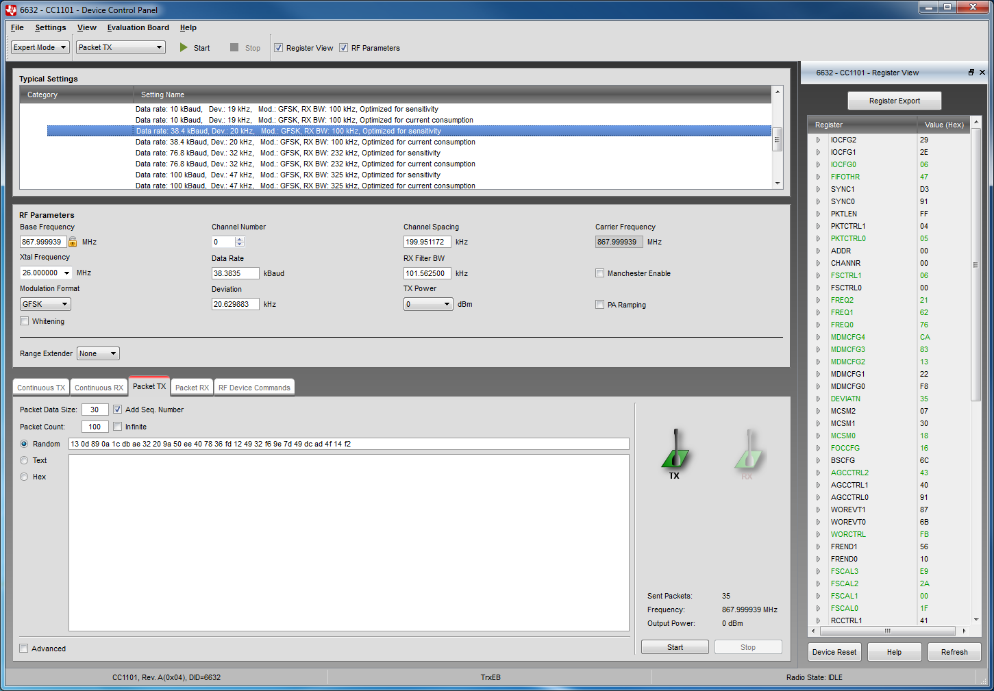
Figure 24. CC1101 configuration NRZ
On CC1310:
- Select the 50 kbps setting. Change the datarate and deviation to the same as CC1101 uses.
- CC1101 uses a 16 bit sync word that is repeated to generate a 32 bit sync word. On CC1310 the sync word then has to be set to 0xD391D391.
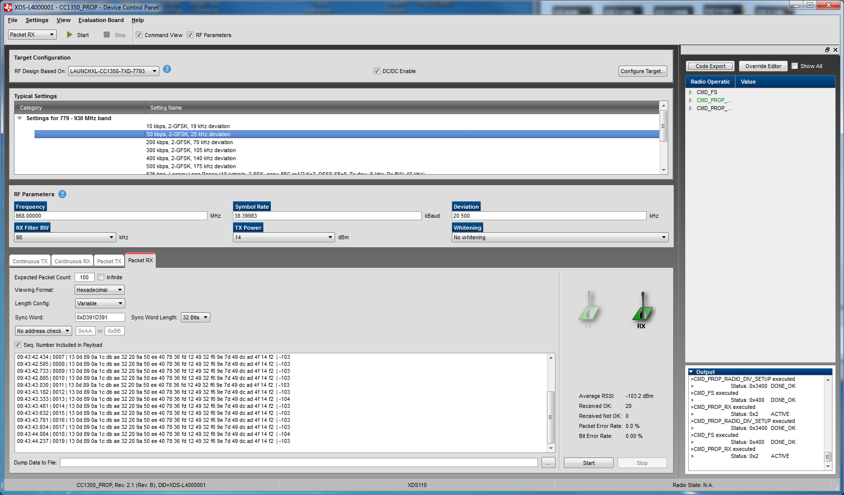
Figure 25. CC1310 configuration NRZ
CC1101 <-> CC1310 using Manchester coding
- On CC1101:
- Select the predefined 38.4 kbps setting
- Tick the Manchester Enable box
- Set MDMCFG2.SYNC_MODE = 2.
On CC1310:
- Select the 50 kbps setting. Change the datarate and deviation to the same as CC1101 uses.
- CC1101 does manchester coding on preamble and sync word, CC1310 only do manchester coding on the payload. The CC1101 sync word manchester encoded is 0xA65A9656. Set the CC1310 synword equal to this.
- Enable manchester by setting PROP_RADIO_DIV_SETUP.formatConf.fecMode = 0xA
- Enable manchester by changing the MCE_RF_OVERRIDE to MCE_RFE_OVERRIDE(0,5,0,1,0,0)
- The following overide has to be added to get the bytes in the correct order: HW_REG_OVERRIDE(0x52B4,0x270C)
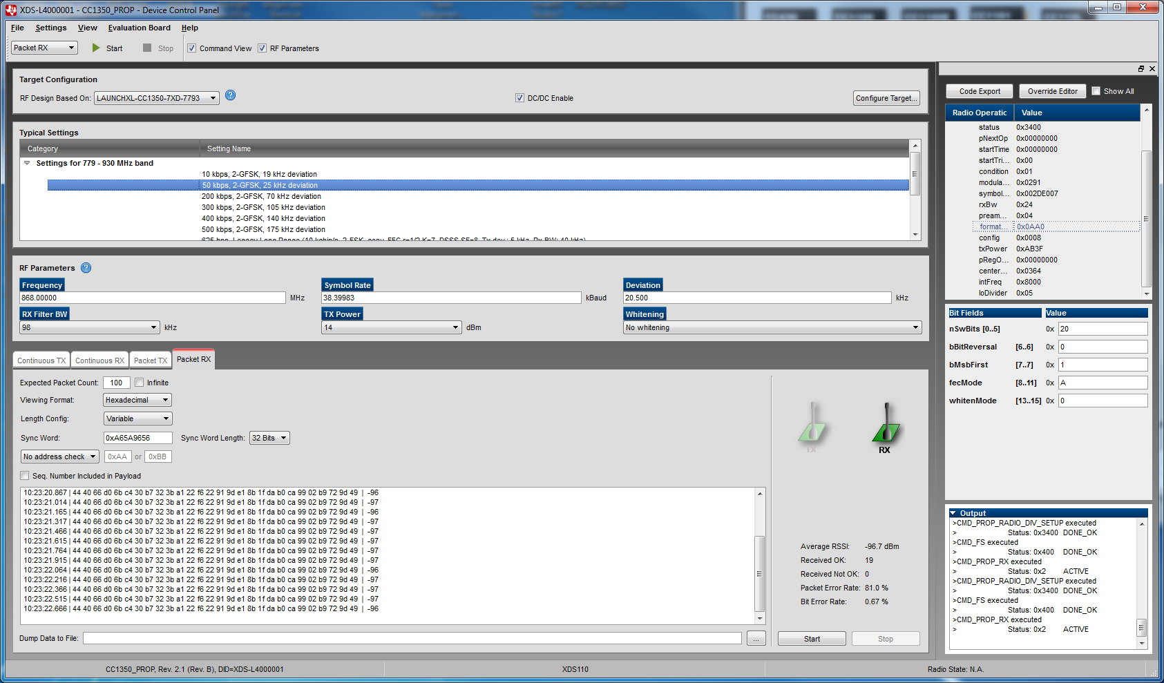
Figure 26. CC1310 configuration manchester
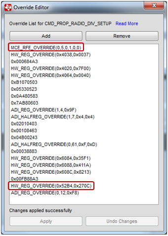
Figure 27. CC1310 override editor manchester
The strict sync word check in CC1310 is not in use when using manchester coding. To reduce the number of false syncs the sync threshold could be increased. See sync_word_qualifier for details.
General note: It is recommended to use manchester only for legacy systems.
How to use the override editor in SmartRF Studio is described in the built-in help in the program.
“Where are my registers?”
CC1101 is a transceiver meaning that to make an application CC1101 has to be used together with an MCU. This MCU communicate with CC1101 over an SPI interface and hardware registers on CC1101 has to be written or strobe commands has to be sent to make the radio do anything.
CC1310 is a wireless MCU. This mean that CC1310 is a power full MCU with a selection of periphery modules where one of these is the RF core. CC1310 still have registers but most of them are hidden from customers. One of the reasons for this is that the meaning of a register on CC1310 changes dependent on which firmware that is running. Instead the communication with the different modules on CC1310 is done via APIs and overrides. All the available modules on CC1310 have a driver. The APIs for the drivers are described in the documentation.
In addition all drivers are documented in the .h files. The .h files also contain examples of usage. The driver .h files could be found here. Some drivers also have examples included in the SDK. See examples.
An override is a register write. Most of the overrides are provided by TI and should not be changed. These are typically registers setting up one or more internal modules and are the result from a lot of testing. The registers users can change freely are typically documented here. Required overrides are given by SmartRF Studio.
“How do I make CC1310 do anything”: Drivers and software
To control CC1101 you can use anything from a simple 8 bits MCU to a multi core Arm processor, all depending on the complexity of your application. CC1310 is a wireless MCU with more than one core hence programming CC1310 is different compared to using a simple 8 bit controller. CC1310 has a number of internal voltage and clock domains. To use (as an example) the RF core the clocks used by the RF core has to be turned on and the voltage domain the RF core is powered from has to be turned on. When the RF core is not in use the clocks and the voltage domain should be turned off to save power. The power on and off needs to be done in a given sequence to ensure that everything is in the correct state.
To simplify the use of CC1310 drivers are available. The driver sets up the clock and power domains and offer an API. The driver documentation could be found here:
The drivers are written in c and it is therefore possible to walk through the code to get a better understanding of what a given driver does if this is wanted and/ or required. In addition, this document describes the power driver requirements: Power Management Software Development Reference.
Both the TI-RTOS and the nonRTOS solution go to the IDLE state whenever possible. In IDLE state the Power_idleFunc() is called which takes the chip to the lowest power state possible.
For a comprehensive TI-RTOS course, see TI RTOS workshop series
The nonRTOS solution is documented here: NoRTOS Driver Porting Layer
EasyLink is a simple abstraction on top of the CC1310 drivers which can be used as a starting point for simple RF protocols. Examples are available in the SDK.
For CC1310 a Software Development Kit (SDK) is provided (SDK download). The 15.4-Stack is included as part of the SDK. Documentation of the stack can be found as part of the SDK documentation.
CC1310 has a part of flash called Customer Configuration. The CCFG parameters are set at compile time in the ccfg.c file in the SDK. The ccfg.c file contains settings for (not a complete list):
- CCFG_FORCE_VDDR_HH: Sets it 12.5 dBm or 14 dBm is maximum output power.
- SET_CCFG_MODE_CONF_DCDC_ACTIVE: Sets if the DCDC should be used in active or not.
- SET_CCFG_MODE_CONF_SCLK_LF_OPTION: Sets the source for the low frequency clock.
- SET_CCFG_MODE_CONF_XOSC_CAP_MOD: Sets if the internal crystal load capacitor array should be used. The default is that the internal array is in use.
- SET_CCFG_EXT_LF_CLK_DIO: The DIO used if using an external clock source for the LF
- SET_CCFG_BL_CONFIG_BL<>: Settings for the bootloader.
“I use feature <> on CC1101, how do I do it on CC1310?”
This part of the migration guide aims to describe how CC1101 features map to the CC1310. The numbering of the sections follows the CC1101 datasheet. If you wonder on how to implement a given thing on CC1310, find which section in the CC1101 datasheet this is covered and look up the section number in the guide.
4 Electrical Specifications
4.1 Current Consumption
The CC1310 current consumption numbers are summarized in 5.4 and 6.7 in the CC1310 Datasheet.
| State | CC1101 | CC1310 |
|---|---|---|
| Tx (10 dBm) | 30.0 mA | 13.4 mA |
| Rx | 14.7 mA | 5.5 mA |
| Sleep | 0.2 uA | 0.2 uA |
4.2 Receive Section
The CC1310 receive parameters are stated in 5.6 and 5.7 in the CC1310 Datasheet.
4.3 RF Transmit Section
The CC1310 transmit parameters are stated in 5.8 and 5.9 in the CC1310 Datasheet.
4.4 Crystal Oscillator
CC1310 has 2 crystal oscillators, 24 MHz and 32.768 kHz. The internal 32.768 kHz RC oscillator can be used instead of the 32.768 crystal. This is done in the ccfg.c file.
4.5 Low Power RC Oscillator
The CC1310 32 kHz RC oscillator is covered in 5.19.3.4 in the CC1310 Datasheet.
4.6 Frequency Synthesizer Characteristics
The CC1310 PLL parameters are covered in 5.10 in the CC1310 Datasheet.
4.7 Analog Temperature Sensor
The CC11310 has a build in temperature sensor and battery monitor.
A API is provided, see AONBATMON
Section 18 in the CC1310 TRM describes how the module is implemented on CC1310.
4.8 DC Characteristics
The CC1310 DC characteristics are covered in 5.17 in the CC1310 Datasheet.
4.9 Power-On Reset
CC1310 has built in power supply supervision that ensures that the chip first starts when the supply voltage to the chip has a valid level. When the voltage drops below a given voltage the voltage supply supervision module take the chip down in a controlled reset to ensure that the chip does not enter an undefined state.
In the ccfg.c file it’s possible to set the reset level to 1.78 V (1.65 V if external regulator mode is used) or 2.0 V, see SET_CCFG_MODE_CONF_VDDS_BOD_LEVEL in the ccfg.c.
5 Pin Configuration
See section 4 in the CC1310 Datasheet to find the CC1310 pin configurations. CC1310 comes in 3 different packet sizes (4x4, 5x5 and 7x7) where the main difference between the packet sizes is the number of available IOs. This is described in more detail in Running the SDK on custom boards.
6 Circuit Description
See the CC1310 Datasheet and section 1 in the CC1310 TRM
7 Application circuit
This section will not cover the CC1310 application circuit but some of the differences between CC1101 and CC1310. For CC1310 application circuits see under Design files under CC1310 Technical Documents.
7.1 Bias Resistor
CC1310 doesn’t use an external bias resistor
7.2 Balun and RF Matching
Similar to CC1101, CC1310 has differential RF pins, RF_P and RF_N. In addition the RXTX pin may be used. The LNA can be biased internally or externally. Ff the latter is the case the RXTX pin is used. In addition, the RF_P and RF_N pins are possible to use single ended. Possible use cases are two single ended paths on two different frequencies or one path for TX and one for RX. The latter could typically be the case when using a FEM.
For 868 MHz, it is also possible to use an IPC instead of discrete components.
7.3 Crystal
CC1301 has a build-in capacitor array used as load capacitors for the crystal. The built in is possible to adjust.
7.4 Reference Signal
CC1310 can only be used with a crystal. TCXO or an external reference signal is not supported.
7.5 Additional Filtering
Not applicable for CC1310. Please follow the reference design under CC1310 Technical Documents.
7.6 Power Supply Decoupling
It is important that the power decoupling is done as in the reference design. In addition the network connected to the DCDC_SW pin should be done as close as possible to the reference design if the DCDC converter is used. Pay close attention to the grounding and to have a short as possible return path from the decoupling to the die paddle.
7.7 Antenna Considerations
Please take a look the CC-Antenna-DK2 and Antenna Measurements Summary for the latest recommended PCB antennas.
7.8 PCB Layout Recommendations
The layout considerations for CC1101 are also valid for CC1310. See the CC1310 datasheet, the reference designs and your manufacturer on solder paste coverage. See the CC1310 reference designs on the number of vias under the chip.
8 Configuration Overview
CC1101 is a transceiver where the transitions between the different states are controlled by a hardware module.
CC1310 is a wireless module where the radioradio is one of the peripherals. The states on CC1101 can therefore not be compared directly. 6.7 in the CC1310 Datasheet describe the main power modes.
The RF driver controls which state the RF core is in.
9 Configuration Software
It’s highly recommended to use the code export feature in SmartRF Studio to get the recommended settings.
For details, press help in SmartRF Studio and scroll down to “Command Code Export” in the contents pan.
10 4-wire Serial Configuration and Data Interface
CC1101 is programmed and controlled over a SPI interface. This section of the CC1101 datasheet covers how to use the SPI interface. The CC1310 is a wireless MCU and therefore is not directly controlled over an interface. Programming the CC1310 is done over the JTAG interface using XDS100V3, XDS110 or XDS200. The CC1310 Launchpad has a built-in XDS110 that can be used to program the CC1310 on the Launchpad or on a custom board using either Flash Programmer 2 or Uniflash.
11 General Control and Status Pins
The pins described in this section of the CC1101 datasheet are related to the SPI interface controlling CC1101. Since CC1310 is controlled differently than CC1101, CC1310 doesn’t have the pin control described in this section of the CC1101 datasheet.
12 Data Rate programming
On CC1101 the wanted data rate is set by writing to the MDMCFG3.DRATE_M and MDMCFG4.DRATE_E registers. On CC1310 the data rate is set via the CMD_PROP_RADIO_DIV_SETUP command. See 23-139 in CC1310 TRM for details. It is recommended to use SmartRF Studio to calculate the required values and export the code. SmartRF Studio also contains a set of characterized settings for data rates used in CC1101 systems. See also settings for different PHYs.
13 Receiver Channel Filter Bandwidth
Receiver bandwidth is set via the CMD_PROP_RADIO_DIV_SETUP command. On CC1310 the RX BW can’t be set independently of the data rate, please see Data rate vs RxBw for more details.
14 Demodulator, Symbol Synchronizer and Data Decision
14.1 Frequency offset compensation
When using (G)FSK and datarates under 500 kbps the frequency offset estimate is available as DEMMAFC0[7:0] / 64 * f_dev; f_dev is the programmed deviation and has unit Hz.
DEMMAFC0[7:0] is on address 0x4004 5154 and should be read after a packet is received. The result is a signed value.:
 //frequency_dev is the deviation given in Hz.
 static int16_t offset  = 0;

 rfc_CMD_READ_RFREG_t RF_cmdReadRfregFreqOffset =
 {
    .commandNo  = 0x0601,
    .address = 0x5154,
    .value = 0,
 };

RF_runImmediateCmd(rfHandle, (uint32_t*)&RF_cmdReadRfregFreqOffset);

offset = (RF_cmdReadRfregFreqOffset.value) * frequency_dev/ 64;
14.2 Bit synchronization
From a user standpoint this is done in the same way on CC1101 and CC1310
14.3 Byte synchronization
From a user standpoint this is done in the same way on CC1101 and CC1310
15 Packet Handling Hardware Support
15.1 Data Whitening
CC1310 can be set up to use the same whitening as CC1101 by setting CMD_PROP_RADIO_DIV_SETUP.whitenMode = 0x1.
15.2 Packet Format
The CC1310 standard packet format shown in figure 23-9 in CC1310 TRM is the same packet format as used on CC1101, but the packet format on CC1310 is made more flexible.
The length of the preamble is possible to set in CMD_PROP_RADIO_DIV_SETUP.nPreamBytes with the possibility to set length of the preamble to most values between 1 - 32 byte in addition to 1 and 4 bit. See table 23-139 for details. On CC1310 it’s possible to use other preambles than 0xAA or 0x55.
The preamble can be set using Overrides:
//Preamble: 0x33
(uint32_t) 0x33330043

//Preamble: 0xCC
(uint32_t) 0xCCCC0043
The length of the sync word is possible to set in CMD_PROP_RADIO_DIV_SETUP.nSwBits with the possibility to set number of bits from 8 to 32.
Note that the CC1101 sync search is purely bit based (the bits in the received data stream are compared one by one with the programmed sync word). CC1310 on the other hand uses a combination of correlator based sync search and a bit based search (strict sync search). A correlator based sync search compare patterns and does not limit sensitivity. This difference in how the CC1101 and CC1310 search for sync cause that it’s not possible to accept 1 bit error pr 16 bits on CC1310 as on CC1101 (MDMCFG2.SYNCMODE). Since the sync search on CC1310 doesn’t limit sensitivity there is no need for a 15/16 or 30/32 sync mode setting on CC1310.
Note that by using CMD_PROP_RX_ADV it is possible to search for two different sync words at the same time.
- CMD_PROP_RX supports up to 255 byte payload, CMD_PROP_RX_ADV supports unlimited length (CMD_PROP_RX_ADV.maxPktLen = 0).
- Fixed or variable packet length is set in CMD_PROP_TX.bVarLen. When using variable packet length mode on CC1101, the length byte must be written to the TX FIFO. On the CC1310, the length byte is not part of the packet but is set through the API (CMD_PROP_TX.pktLen).
15.3 Packet Filtering in Receive Mode
Address filtering can be enabled by setting CMD_PROP_RX.bChkAddress. The received address is compared against CMD_PROP_RX.address0 and CMD_PROP_RX.address1. CRC filtering can be enabled by setting CMD_PROP_RX.bUseCrc
16 Modulation Formats
As of today CC1310 supports 2-(G)FSK and OOK. Contact TI if you need a different format.
17.1 Sync Word Qualifier
The sync word is selectable to have a length from 8 bits to 32 bits. This is set in CMD_PROP_RADIO_DIV_SETUP.nSwBits. The syncword threshold could be set with the following override:
HW_REG_OVERRIDE(0x5104,0xYYZZ)
where YY and ZZ is the threshold for the two correlators. For simplicity the two threshold could be set equal. Higher value is stricter. The default sync threshold is given by:
Sync Threshold = (30*nSwBits)/32 + 9
17.2 Preamble Quality Threshold (PQT)
The CMD_PROP_CS command can be used to monitor the RF activity in a channel and return busy if a preamble is present.
If PQT gating of sync search is wanted CMD_PROP_RX_SNIFF has to be chained (Conditional execution and chaining) with CMD_PROP_RX.
17.3 RSSI
If in Rx, the function RF_getRssi() returns the RSSI value. After receiving a packet the radio will no longer be in RX mode unless bRepeatOk = 1. The RSSI of a received packet can be read from the rfc_propRxOutput_t struckture.
In the code, add:
static rfc_propRxOutput_t rxStatistics;
int8_t RSSIout;

// Under Modify CMD_PROP_RX command for application needs
RF_cmdPropRx.pOutput = (uint8_t*)&rxStatistics;

// Where you want to read out the RSSI in the code
RSSIout = rxStatistics.lastRssi;
17.4 Carrier Sense (CS)
The CMD_PROP_CS command can be used to monitor the RF activity in a channel and return busy if the RSSI is above a given threshold.
17.5 Clear Channel Assessment (CCA)
The rfListenBeforeTalk example in the CC1310 SDK (readme) show how LBT or CCA can be implemented.
17.6 Link Quality Indicator (LQI)
It is not possible to output the LQI via the rfc_propRxOutput_t structure or to append it to the packet meta data.
The LQI for the last received packet when using genfsk can be read from a register if the RF core is not in RX.:
static uint8_t LQI  = 0;

rfc_CMD_READ_RFREG_t RF_cmdReadLQI =
{
  .commandNo  = 0x0601,
  .address = 0x5268,
  .value = 0,
};

RF_runImmediateCmd(rfHandle, (uint32_t*)&RF_cmdReadLQI);

LQI = (RF_cmdReadLQI.value);
18.1 Forward Error Correction (FEC)
A patch enables a CC1101 compatible FEC on CC1310. The patch is at the moment not released.
19.1 Power-On Start-Up Sequence
The CC1310 has a build in POR/ BOD that ensures that the chip does not boot up before VDDS is above the set minimum voltage (power_on_reset). The chip also has an external reset pin. Follow the reference design for an external circuit that ensures a pin reset at power-up.
19.2 Crystal Control
The 24 MHz XOSC is controlled by the drivers. A user doesn’t need to write code that directly controls the 24 MHz XOSC.
19.3 Voltage Regulator Control
The voltage regulators are controlled by the chip.
19.4 Active Modes (RX and TX)
The RF core has two active states, RX and TX.
- The CMD_PROP_TX and CMD_PROP_TX_ADV commands set the radio in TX sending a packet(s) placed in the packet (or TX queue) the command point to.
- The CMD_TX_TEST sets the radio in TX and a CW or a 16 bit Tx word is sent continuously until the endTrigger or an abort command is issued.
- The CMD_PROP_RX and CMD_PROP_RX_ADV commands sets the the radio in Rx to receive a packet. The command exits Rx when the endTrigger is reached or a packet is received (optional).
- The CMD_PROP_CS commands sets the radio in RX to check if the RSSI is above a threshold or if a preamble is detected (PQT).
- The CMD_PROP_RX_SNIFF and CMD_PROP_RX_ADV_SNIFF set the radio in Rx and combines the CMD_PROP_CS with normal packet receiption.
- The CMD_RX_TEST sets the radio in RX for test purposes
The CMD_PROP_RADIO_SETUP and CMD_FS command have to be issued before sending one of the commands above to start and calibrate the VCO/ PLL, turn on the needed clocks, do patching and to configure the radio.
The radio commands are described in section 23 in the CC1310 TRM. Some information could also be found in the description of the RF core.
19.5 Wake On Radio (WOR)
Wake On Radio is shown in the example (rfWakeOnRadioRx). This example uses the CMD_PROP_RX_SNIFF command.
19.6 Timing
The MCU timing is given in 5.19.2 in the CC1310 Datasheet. The time to turn on the radio code and go either to RX or TX or TX <-> RX is not fixed. Part of the time is related to software and therefore the time will be dependent on how many and which patches are used. To get an accurate number the timing should be measured with the software intended to run on the device. The RF core signals intended to control an external LNA or PA could be used to measure the timing.
19.7 RX Termination Timer
The CMD_PROP_RX and CMD_PROP_RX_ADV have endTime as a parameter. Start and End Triggers gives an overview over the possible triggers.
20 Data FIFO
Data queues are used for transferring packets from the RF core to the main CPU and vice versa. For documentation, see:
- The software examples in the SDK
- Data Queues.
- 23.4 in CC1310 TRM.
21 Frequency Programming
The RF frequency needs to be given as input to two commands:
CMD_PROP_RADIO_DIV_SETUP:
- centerFreq: Center frequency of the band.
CMD_FS: Sets up the frequency synthesizer, described in 23.3.3.1.5 in CC1310 TRM.
- The frequency is given in two parts:
- frequency: Given in MHz
- fractFreq: Fractional part of the frequency
If the frequency given in the CMD_FS command is different from the frequency given in the CMD_PROP_RADIO_DIV_SETUP command some parameters parameters will then have been calculated with a relative error of up to: (freq - centerFreq)/ centerFreq. Deviation is one of the parameters that will be scaled with this factor. If this error is acceptable it is possible to do frequency hopping in the 863 MHz - 870 MHz band by setting the center frequency in the middle of the band, 867 MHz, using CMD_PROP_RADIO_DIV_SETUP once and the CMD_FS to set the frequencys when hopping.
SmartRF Studio can be used to calculate the frequency word.
22 VCO
The CMD_FS command starts and calibrate the VCO. On CC1310 a CMD_FS has to be run for every frequency. It is not possible to pre-calibrate each channel.
23 Voltage Regulators
As with the CC1101, the CC1310 contains internal regulators that are invisible for customers.
The battery voltage on CC1310 is called VDDS (allowed level 1.8 V to 3.8 V). The output of the global LDO/ internal DCDC converter is called VDDR. When the DCDC is in use the VDDR net should not be connected to anything else than the external components shown in the reference designs. The Power Supply System is described in more detail in 1.3.13 in CC1310 TRM.
Note that on CC1310 it is possible to run different DIO segments on different voltages; see 11.10.2 Digital Input/ Output Power Domains in CC1310 TRM.
24 Output Power Programming
The wanted output power is set in CMD_PROP_RADIO_DIV_SETUP.txPower. Max output power is dependent on the setting in ccfg.c.
Most PAs have temperature dependent output power. On CC1310 it is possible to compensate for the temperature dependency and get an output power that is close to independent of temperature. The txPower settings found in SmartRF Studio contain the temperature compensation. This compensation is only valid for boards that follow our reference design closely. If a custom board does not follow the reference design the output power will be different and the temperature compensation coefficients have to be calculated for the custom board. See 23.3.4.16 in CC1310 TRM for equations.
For OOK the output power is set by Overrides
Example: To set 13.0 dBm:
HW_REG_OVERRIDE(0x6098,0x7000)
| Override | Output power @ 25 Degree C |
|---|---|
| 0x6098,0x7200 | 14.0 |
| 0x6098,0x7100 | 13.4 |
| 0x6098,0x7000 | 13.0 |
| 0x6098,0x6F00 | 11.5 |
| 0x6098,0x6E00 | 9.5 |
| 0x6098,0x6D00 | 7.5 |
| 0x6098,0x6C00 | 5.2 |
| 0x6098,0x6B00 | 3.6 |
| 0x6098,0x6A00 | 1.4 |
| 0x6098,0x6900 | -1.8 |
| 0x6098,0x6800 | -7.2 |
| 0x6098,0x6700 | -8.9 |
| 0x6098,0x6600 | -10.8 |
| 0x6098,0x6500 | -13.0 |
| 0x6098,0x6400 | -15.7 |
| 0x6098,0x6300 | -19.0 |
| 0x6098,0x6200 | -22.8 |
| 0x6098,0x6100 | -27.3 |
The numbers are an indication of which output power to expect when CCFG_FORCE_VDDR_HH=‘1’.
25 Shaping and PA Ramping
When using (G)FSK PA ramping is included in the examples.
26 General Purpose / Test Output Control Pins
- Signal routing describes how to get some internal signal available on external pins.
- Packet format contains some more information on how to use of the internal signals to debug packet formats.
27 Asynchronous and Synchronous Serial Operation
An asynchronous signal (MCE_GPO1) is available in RX, see signal routing. This signal is the sign of the instantaneous frequency. This signal is used as input to further data processing and therefore measuring PER will give better sensitivity compared to looking at the asynchronous output.
It is only possible to get one signal from the RF core. It is therefore not possible to generate a clock at the same time as getting the data out.
For Tx it is not possible to apply an external bit stream to CC1310 to be sent on the air. By using the TX buffer and the CMD_PROP_TX/ CMD_PROP_TX_ADV commands it is possible to generate the data wanted to send. It is not possible to turn off preamble (minimum 1 bit) and sync (minimum 8 bit). If the protocol is not using a sync word the sync word can be set equal to the first 8 bit of the payload.
28.2 Frequency Hopping and Multi-Channel Systems
The 15.4 Stack shows how frequency hopping can be implemented. On CC1310 a CMD_FS has to be run for every frequency. It is not possible to pre-calibrate each channel.
28.3 Wideband Modulation when not Using Spread Spectrum
An application note will be released to cover this.
28.4 Wireless MBUS
CC1310 has full support for C, T and S mode. Documentation is available in Combined wM-Bus C-Mode and T-Mode and wM-Bus S-Mode
28.7 Battery Operated Systems
CC1310 is designed to be used in battery operated system with very low standby current and low active current. The drivers ensure that the chip is in the state that gives lowest power consumption at any given time.
28.8 Increasing Range
For increased range (better sensitivity and higher output power), CC1310 can be used together with CC1190 (CC1190 Datasheet). See Using CC1190 Front End With CC13xx Under EN300220 and Using CC1190 Front End With CC13xx Under FCC 15.247.
29 Configuration Registers
On CC1101 writing/ reading registers are required to operate the chip. On CC1310 the control of the radio core is done by using drivers and APIs. Therefore no description is given of registers on CC1310.
Words and expressions
genfsk: Used as an abbreviation for settings that uses the patch rf_patch_cpe_genfsk. genfsk supports up to 500 kbps FSK and GFSK.
Strick sync word search: The received sync word has to be bit by bit equal to the programmed sync word.