6.3.7. EVMK2H Hardware Setup Guide
6.3.7.1. Hardware Setup
Note
The EVM board is sensitive to electrostatic discharges (ESD). Use a grounding strap or other device to prevent damaging the board. Be sure to connect communication cables before applying power to any equipment.
6.3.7.1.1. FTDI Driver Installation on PC Host
The K2 EVM has a FTDI FT2332HL device on board. A driver must be installed on the PC Host in order to be able to communicate with the EVM using the FTDI mini-USB connector located under the mini-USB connector of the emulator daughter card. The driver can be downloaded from here FTDI Driver.
Note
Before testing the usb connection, make sure that the mini-usb cable is plugged into the port on the base board. (and not connected to the daughter card).
After installing the driver and connecting the USB cable, two COM ports should be visible in the list of COM ports available to connect to in the PC Host terminal console. The lower COM port corresponds to the SoC UART and the higher one corresponds to the MCU UART.
6.3.7.1.2. BMC Version Check and Update
Read BMC_In-Field_Update to check BMC version and update if necessary.
6.3.7.1.3. UCD Power Management Modules In-Field Update
There are three power management modules (sometimes called the UCDs)
located on the EVM. Each module can be identified by it’s address:
104(68h), 52(34h), and 78(4Eh). Each module contains non-volatile
registers that determine it’s operation. It may be necessary to update
these registers after the board has been shipped. This update can be
performed through the BMC, which can issue commands to the UCD modules
to update the register settings. The Power Management Configuration
Update Tool (bmc_tool.py) performs the task of sending commands to
the BMC to get the current module versions, and perform updates using
configuration files. Instructions for executing the update tool
(bmc_tool.py) are available here: BMC Tool UCD Update Guide
The latest version of the tool is available here. The latest configuration files (txt files) are available here. Please follow the instructions provided to check the current module versions, and update them accordingly.
Note
The DIP switch configuration of the board when running the update is irrelevant.
Note
BMC versions 1.0.1.3a and earlier will not work properly with the Get Versions feature of the Update Tool. Upgrade to a more recent version of the BMC to use this functionality.
6.3.7.1.4. Attach the Ethernet cable
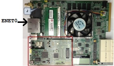
Using the Ethernet cable supplied, connect one end of the cable to the Ethernet Port 0 (marked ENET0 on the board) on the EVM and the other end to your PC.
This picture shows which Ethernet Port is 0:
6.3.7.1.5. Connect the JTAG interface
Use the USB to USB mini-B cable provided. Connect the USB mini-B connector to the USB mini-B interface on the XDS-2xx daughter card on the EVM, and the USB connector to your PC. This enables XDS-2xx emulation and is directly useable by CCS. If you are using a different JTAG, connect it now.
6.3.7.1.6. K2H Set the boot mode switch SW1
K2H No Boot/JTAG DSP Little Endian Boot mode
For Rev 0B EVM, the setting is as follows
SW1 - 4(ON) 3(ON) 2(ON) 1(OFF)
For Rev 1.0 EVM, the setting is as follows:
SW1 - 1(OFF) 2(OFF) 3(OFF) 4(ON)
K2H SPI Little Endian Boot mode
For Rev 0B EVM, the setting is as follows:
SW1 - 4(ON) 3(ON) 2(OFF) 1(ON)
For Rev 1.0 EVM, the setting is as follows:
SW1 - 1(OFF) 2(OFF) 3(ON) 4(OFF)
6.3.7.1.7. DDR Configuration (Rev 0B EVM only)
For Rev 0B EVM, the following procedure is required for proper DDR configuration:
- Connect the MCU UART port to PC using the serial cable provided with the EVM. The MCU UART port is the 4-pin white connector farthest from the edge of the EVM. Alternatively it is also possible to connect a mini-USB cable to the FTDI mini-USB connector of the EVM. This will provide access to both the SoC and the MCU UART ports.
- Start Tera Term or Hyper terminal and set to 115200 board rate, 8-bit data, 1-bit stop and no parity/flow control.
- Power on the EVM. MCU UART console will show user prompt once MCU boot up is complete. Type the following commands at the console to setup DDR3A. Ethernet requires DDR3A and will not work with DDR3B which is default in Rev 0B EVMs.
BMC> setboot 100001
BMC> fullrst
6.3.7.1.8. Attach the serial port cable to the SoC UART port
Connect the SoC UART port to PC using the serial cable provided with the EVM. The SoC UART port is the 4-pin white connector closest to the edge of the EVM.
Start Tera Term or Hyper terminal and set to 115200 board rate, 8-bit data, 1-bit stop and no parity/flow control.
6.3.7.1.9. Connect the power cable
Connect the power cable to the EVM power jack on the board. To be ESD safe, plug in the other end of the power cable only after you have connected the power cord to the board. Then turn on the board.
6.3.7.2. BMC In-Field Update
BMC, or Board Management Controller, takes care of the power, clocks, resets, bootmodes, etc. of the EVM.
For Rev1.0 EVMs an in-field update may be necessary as a very small quantity were delivered with an old revision of the BMC. If your EVM is using version 1.0.1.3 then it should be updated to version 1.0.1.3a. The update corrects the way that the boot mode pins are interpreted.
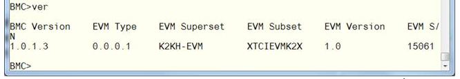
You can check the version by:
1. Opening a hyperterminal or another similar type of console application.
2. Set COM Port to higher value
- When you connect to FTDI mini-USB on the EVM it will provide 2 COM port connections, one to the SOC UART and one to BMC UART.
- The SOC UART will always be the lowest value COM port, for example COM5, and the BMC UART will always be the higher value COM port, for example COM6. (Actual COM PORT values will vary).
3. Set COM port properties appopriately:
- Baud Rate or Bits per second: 115200
- Data Bits: 8
- Parity: None
- Stop Bits: 1
- Flow Control: None
4. At BMC prompt typer ‘ver’ (no quotes)
5. Check BMC Version
If an in-field update is needed, downloaded the latest version here (labeled Board Management Controller Binaries (BMC)) and continue with the following steps.
Prepare EVM for in-field update:
- Remove power to the EVM.
- Set boot mode to “No Boot mode” ( See NoBootLittleEndian_ )
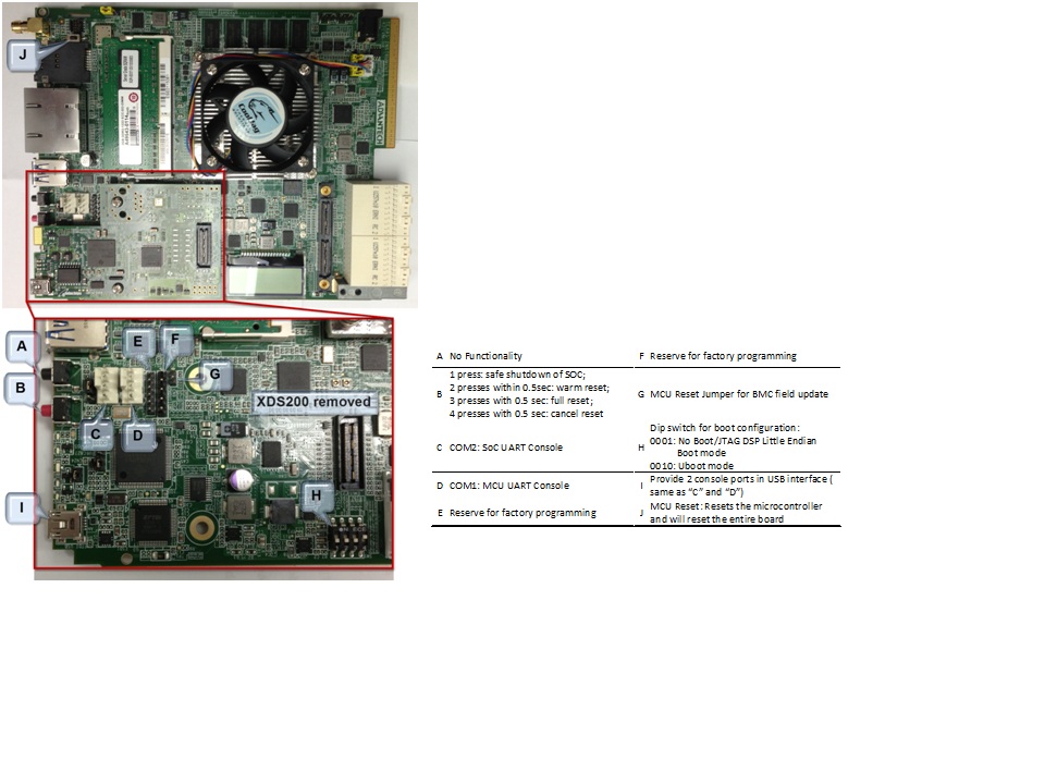
- Remove the MCU_BOOTSELECT (CN9) jumper (see picture below for location of jumper: Referred as “G: MCU Reset Jumper for BMC field update”).
- Make sure your USB cable is connected to FTDI mini-USB (not XDS200 Emulator USB) OR connect 4pin UART cable to COM1: MCU UART connector.
- Make sure no HyperTerminal/Console connected to BMC COM port are open or active.
- Use the LM Flash Programmer (available here) to update the firmware, as detailed in the steps below.
Perform in-field update:
Apply power to the EVM. No LED’s will be illuminated and no LCD backlight or characters will be on because the BMC is waiting for a command rather than executing from Flash.
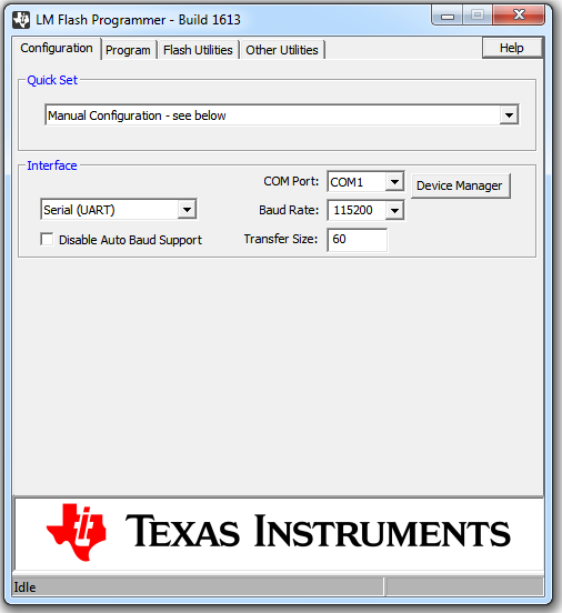
Open the LM Flash programmer utility. (Default location Start Menu -> All Programs -> Texas Instruments -> Stellaris -> LM Flash Programmer -> LM Flash Programmer )
In the LM Flash Programmer Utility ‘Configuration’ tab, in the interface section, select ‘Serial (UART)’ from the drop-down box on the left.
Select the BMC COM Port (the same COM port used to issue the ver command earlier), and set the ‘Baud Rate’ to 115200.
Set ‘Transfer Size’ to 60, and make sure ‘Disable Auto Baud Support’ is unchecked.
In the ‘Program’ tab, Browse to the location of the binary file containing the firmware update, and select it.
Leave all other options as default, and press the ‘Program’ button.
After the programming is complete, power off the board.
Reconnect the jumper.
Open the HyperTerminal/Console for the BMC COM port.
Apply power to the EVM. When BMC completes initialization of board it will show latest version of BMC in Console.
If step 9 was done after power was applied, just type “ver” at BMC prompt.
6.3.7.3. DIP Switch and Bootmode Configurations
6.3.7.3.1. Rev 1.0 EVM SW1 switch Bootmode Configuration
| DIP Switch (p1, p2, p3, p4) | Bootmode |
|---|---|
| 0000 | ARM NAND |
| 0001 | DSP no-boot |
| 0010 | ARM SPI |
| 0011 | ARM I2C |
| 0100 | ARM UART |
| 0101 | Reserved |
| 0110 | Reserved |
| 0111 | Reserved |
| 1000 | Reserved |
| 1001 | Reserved[1] |
| 1010 | Reserved |
| 1011 | Reserved |
| 1100 | Reserved |
| 1101 | Reserved |
| 1110 | Reserved |
| 1111 | Reserved |
[1]In revision BMC v1.0.1.4 this is 10 MHz SPI NOR. This will not continue in future versions.
6.3.7.3.2. Changing the Bootmode
In BMC v1.0.1.x the only way to use a bootmode that is not supported by the DIP switch combinations is to use the ‘setboot’ and ‘fullrst’ commands. To set the bootmode use the setboot command, which takes a 32 bit value in hex as its only argument:
setboot 00110CE7
Then use the fullrst command to boot the SoC into this bootmode:
fullrst
This process is volatile, and will have to be repeated every time the board is power cycled.
In BMC v1.0.2.x the setboot command has been removed. It has been replaced with the bootmode command, which performs various functions depending on the way in which the command is used. The command works with 16 bootmodes, which are representative of the various DIP switch combinations; the bootmodes are numbered 0 - 15. Bootmodes 8 - 15 are User-Defined, and may be altered and stored using the command (explained below). Each bootmode consists of a title, a high value, and a low value. The high value is currently not used. The low value is a 32 bit value in hex, and is the same as the value previously used by setboot. The bits of low value (and the setboot argument) are shown in the table below).
| Bit | Devstat Bit | Config Pin Function | Normal Pin Function | Comments |
|---|---|---|---|---|
| 31 | Reserved | |||
| 30 | Reserved | |||
| 29 | Reserved | |||
| 28 | Reserved | |||
| 27 | Reserved | |||
| 26 | Reserved | |||
| 25 | PACLKSEL | PACLKSEL | ||
| 24 | CORECLKSEL | CORECLKSEL | ||
| 23 | Reserved | |||
| 22 | AVSIFSEL1 | TIMI1 | Reserved: EVM forces these bits to strap values during reset | |
| 21 | AVSIFSEL0 | TIMI0 | Reserved: EVM forces these bits to strap values during reset | |
| 20 | DDR3_REMAP_EN | GPIO16 | ||
| 19 | ARM_LENDIAN | GPIO15 | 0 = little, 1 = is not supported; do in SW | |
| 18 | MAINPLLODSEL | CORESEL3 | ||
| 17 | ARMAVSSHARED | CORESEL2 | ||
| 16 | 16 | BOOTMODE15 | CORESEL2 | |
| 15 | 15 | BOOTMODE14 | CORESEL1 | Element |
| 14 | 14 | BOOTMODE13 | CORESEL0 | |
| 13 | 13 | BOOTMODE12 | GPIO13 | |
| 12 | 12 | BOOTMODE11 | GPIO12 | |
| 11 | 11 | BOOTMODE10 | GPIO11 | |
| 10 | 10 | BOOTMODE9 | GPIO10 | |
| 9 | 9 | BOOTMODE8 | GPIO9 | |
| 8 | 8 | BOOTMODE7 | GPIO8 | |
| 7 | 7 | BOOTMODE6 | GPIO7 | |
| 6 | 6 | BOOTMODE5 | GPIO6 | |
| 5 | 5 | BOOTMODE4 | GPIO5 | |
| 4 | 4 | BOOTMODE3 | GPIO4 | |
| 3 | 3 | BOOTMODE2 | GPIO3 | |
| 2 | 2 | BOOTMODE1 | GPIO2 | |
| 1 | 1 | BOOTMODE0 | GPIO1 | |
| 0 | 0 | LENDIAN | GPIO0 |
There are 5 different formats to the bootmode command:
bootmode
When the command is entered with no arguments the current bootmode will be displayed.
bootmode all
This format will display all 16 bootmodes and mark the currently selected bootmode.
bootmode #x
This will change the currently selected bootmode to the bootmode represented by x. For example, if the board is booted with DIP switch setting 1(OFF) 2(OFF) 3(OFF) 4(ON) then the bootmode would be 1 - DSP NO-BOOT. If ‘bootmode #2’ is entered, the bootmode represented by DIP switch setting 1(OFF) 2(OFF) 3(ON) 4(OFF) would become the current bootmode (ARM SPI-NOR BOOT). If the ‘reboot’ command is given, the SoC will be rebooted using this new bootmode. This format is volatile, meaning once power is removed, the bootmode at the next power up will be determined by the DIP switch.
bootmode read
This format reads the current value of the DIP switch, and changes the current bootmode to this value. For example, if the board is booted with DIP switch setting 1(OFF) 2(OFF) 3(OFF) 4(ON) then the bootmode would be 1 - DSP NO-BOOT. If the DIP switch is changed to 1(OFF) 2(OFF) 3(ON) 4(OFF) and then the command ‘bootmode read’ is given, the board will change to bootmode 2 - ARM SPI-NOR BOOT. If the ‘reboot command is then given, the SoC will be rebooted using this new bootmode.
bootmode [#]x hi_value lo_value title
This bootmode is used to alter User-Defined bootmodes (bootmodes 8 - 15). x is the index of the bootmode to be set, as such its appropriate value range is 8 - 15, any other value will return an error. hi_value is not currently used, and should always be set to 0. lo_value is a 32 bit hex value whose bits are representative of the table above. title is a given string that is displayed by the bootmode command to help better understand what the bootmode does, it has no purpose within the actual booting of the board. The option ‘#’ is used to determine whether the bootmode will be saved. If # is used, the bootmode will be saved to flash, meaning the new value is tied to the DIP switch, and will remain even if power is removed from the board. If # is not given, then the change will be lost as soon as power is removed. Some examples with descriptions are given below:
bootmode 8 0 112005 ARM_SPI
bootmode 8 will be set to 112005 and given the title ARM_SPI. To boot into this bootmode, the command ‘bootmode #8’ followed by ‘reboot’ would be given (or changing the DIP switch to 1(ON) 2(OFF) 3(OFF) 4(OFF) without removing power, then entering ‘bootmode read’ followed by ‘reboot’). Once power is removed, this change is lost.
bootmode #10 0 12cba1 RANDOM_BOOT
bootmode 10 will be set to 12cba1 and given the title RANDOM_BOOT. This is now the permanent value of bootmode 10; the change will persist even if power is removed.
6.3.7.4. Connect to EVMK2H using CCS
Step 1: Configure the EVM hardware
- Setup the EVM to DSP no boot using SW1 as described in the section BootModeConfiguration
- Connect mini USB cable to the XDS2xx MIPI adapter card marked J1 or connect external emulator to the MIPI connector on J3
Note
For newer versions of CCS, a XDS200 firmware update is recommended which user can perform using instruction on the article
below:
Note
For newer versions of CCS, a XDS200 firmware update is recommended which user can perform using instruction on
Updating_the_XDS200_firmware <http://dev.ti.com/tirex/explore/node?node=AADzJ8Y-La4f7Bi5Ga0TcA__FUz-xrs__LATEST>__
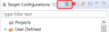
Step 2: Create CCS Target configuration
Launch CCS on your host machine. Select View Tab and select the “Target configuration”
Create New Target configuration in CCS by selecting appropriate emulator. For Default on board emulator select “Texas instruments XDS2xx Debug Probe” and select the target device as 66AK2H12.
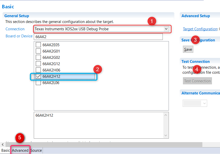
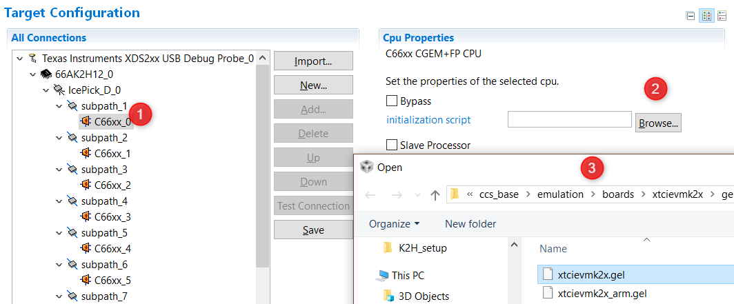
Go to the Advanced Tab where you will see all the cores on the SOC listed. In order to initialize the clocks and external DDR memory on the device, users are required to use a initialization Gel scripts. To populate the Gel Select A15_0 and then hit Browse and locate the GEL in the CCS installation under the following path: CCS_INSTALL/ccs_base/emulation/boards/xtcievmk2x/gel
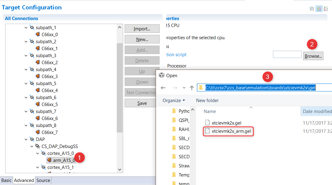
DSP developers, can also select C66x_0 and populate the DSP GEL file that is found in the same location.
Going back to the Basic Tab, Save the configuration. For additional sanity check, you can also test connection.
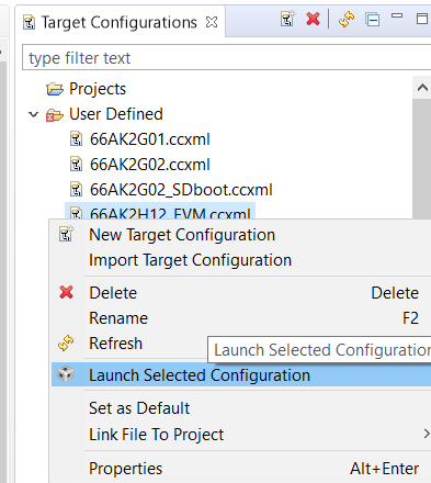
Step 3: Connect to the cores
Right click on the target configuration and Select “Launch Target configuration”. Wait for CCS debug View to launch and display the eight C66x cores and 4 A15 cores.
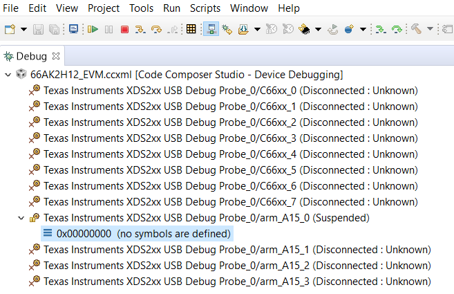
Start by connecting to A15_0 and C66x_0. when you connect to the cores, you will see the GEL script logs in the console window, which indicates that device clocks, PSC and external DDR memory has been initialized. The GEL log from target connect is provided below for reference.
arm_A15_0: GEL Output: Disabling MMU
arm_A15_0: GEL Output: Disabling Caches
arm_A15_0: GEL Output: Invalidate Instruction Caches
arm_A15_0: GEL Output: Enabling non-secure access to cp10 and cp11
arm_A15_0: GEL Output: Enabled non-secure access to cp10 and cp11
arm_A15_0: GEL Output: Enabling SMP bit in ACTLR
arm_A15_0: GEL Output: Enabled SMP bit in ACTLR
arm_A15_0: GEL Output: Entering NonSecure Mode
arm_A15_0: GEL Output: Entered NonSecure Mode
arm_A15_0: GEL Output: Disabling MMU
arm_A15_0: GEL Output: Disabling Caches
arm_A15_0: GEL Output: Invalidate Instruction Caches
arm_A15_0: GEL Output:
Connecting Target...
arm_A15_0: GEL Output: Disabling MMU
arm_A15_0: GEL Output: Disabling Caches
arm_A15_0: GEL Output: Invalidate Instruction Caches
arm_A15_0: GEL Output: Enabling non-secure access to cp10 and cp11
arm_A15_0: GEL Output: Enabled non-secure access to cp10 and cp11
arm_A15_0: GEL Output: Enabling SMP bit in ACTLR
arm_A15_0: GEL Output: Enabled SMP bit in ACTLR
arm_A15_0: GEL Output: Entering NonSecure Mode
arm_A15_0: GEL Output: Entered NonSecure Mode
arm_A15_0: GEL Output: Disabling MMU
arm_A15_0: GEL Output: Disabling Caches
arm_A15_0: GEL Output: Invalidate Instruction Caches
arm_A15_0: GEL Output: TCI6638K2K GEL file Ver is 1.89999998
arm_A15_0: GEL Output: Disabling MMU
arm_A15_0: GEL Output: Disabling Caches
arm_A15_0: GEL Output: Invalidate Instruction Caches
arm_A15_0: GEL Output: Enabling non-secure access to cp10 and cp11
arm_A15_0: GEL Output: Enabled non-secure access to cp10 and cp11
arm_A15_0: GEL Output: Enabling SMP bit in ACTLR
arm_A15_0: GEL Output: Enabled SMP bit in ACTLR
arm_A15_0: GEL Output: Entering NonSecure Mode
arm_A15_0: GEL Output: Entered NonSecure Mode
arm_A15_0: GEL Output: Disabling MMU
arm_A15_0: GEL Output: Disabling Caches
arm_A15_0: GEL Output: Invalidate Instruction Caches
arm_A15_0: GEL Output: Detected PLL bypass disabled: SECCTL[BYPASS] = 0x00000000
arm_A15_0: GEL Output: (3a) PLLCTL = 0x00000040
arm_A15_0: GEL Output: (3b) PLLCTL = 0x00000040
arm_A15_0: GEL Output: (3c) Delay...
arm_A15_0: GEL Output: (4)PLLM[PLLM] = 0x0000000F
arm_A15_0: GEL Output: MAINPLLCTL0 = 0x07000000
arm_A15_0: GEL Output: (5) MAINPLLCTL0 = 0x07000000
arm_A15_0: GEL Output: (5) MAINPLLCTL1 = 0x00000040
arm_A15_0: GEL Output: (6) MAINPLLCTL0 = 0x07000000
arm_A15_0: GEL Output: (7) SECCTL = 0x00090000
arm_A15_0: GEL Output: (8a) Delay...
arm_A15_0: GEL Output: PLL1_DIV3 = 0x00008002
arm_A15_0: GEL Output: PLL1_DIV4 = 0x00008004
arm_A15_0: GEL Output: PLL1_DIV7 = 0x00000000
arm_A15_0: GEL Output: (8d/e) Delay...
arm_A15_0: GEL Output: (10) Delay...
arm_A15_0: GEL Output: (12) Delay...
arm_A15_0: GEL Output: (13) SECCTL = 0x00090000
arm_A15_0: GEL Output: (Delay...
arm_A15_0: GEL Output: (Delay...
arm_A15_0: GEL Output: (14) PLLCTL = 0x00000041
arm_A15_0: GEL Output: PLL has been configured (CLKIN * PLLM / PLLD / PLLOD = PLLOUT):
arm_A15_0: GEL Output: PLL has been configured (122.879997 MHz * 16 / 1 / 2 = 983.039978 MHz)
arm_A15_0: GEL Output: Switching on ARM Core 0
arm_A15_0: GEL Output: Switching on ARM Core 1
arm_A15_0: GEL Output: Switching on ARM Core 2
arm_A15_0: GEL Output: Switching on ARM Core 3
arm_A15_0: GEL Output: ARM PLL has been configured (125.0 MHz * 16 / 2 = 1000.0 MHz)
arm_A15_0: GEL Output:  DISABLESTAT ---> 0x00000000
arm_A15_0: GEL Output: Power on all PSC modules and DSP domains...
arm_A15_0: GEL Output: Power on all PSC modules and DSP domains... Done.
arm_A15_0: GEL Output: WARNING: SYSCLK is the input to the PA PLL.
arm_A15_0: GEL Output: Completed PA PLL Setup
arm_A15_0: GEL Output: PAPLLCTL0 - before: 0x0x09080500  after: 0x0x09080500
arm_A15_0: GEL Output: PAPLLCTL1 - before: 0x0x00002040  after: 0x0x00002040
arm_A15_0: GEL Output: DDR begin
arm_A15_0: GEL Output: XMC setup complete.
arm_A15_0: GEL Output: DDR3 PLL (PLL2) Setup ...
arm_A15_0: GEL Output: DDR3 PLL Setup complete, DDR3A clock now running at 666 MHz.
arm_A15_0: GEL Output: DDR3A initialization complete
arm_A15_0: GEL Output: DDR3 PLL Setup ...
arm_A15_0: GEL Output: DDR3 PLL Setup complete, DDR3B clock now running at 800MHz.
arm_A15_0: GEL Output: DDR3B initialization complete
arm_A15_0: GEL Output: DDR done
arm_A15_0: GEL Output: Entering A15 non secure mode ..
arm_A15_0: GEL Output: Disabling MMU
arm_A15_0: GEL Output: Disabling Caches
arm_A15_0: GEL Output: Invalidate Instruction Caches
arm_A15_0: GEL Output: Enabling non-secure access to cp10 and cp11
arm_A15_0: GEL Output: Enabled non-secure access to cp10 and cp11
arm_A15_0: GEL Output: Enabling SMP bit in ACTLR
arm_A15_0: GEL Output: Enabled SMP bit in ACTLR
arm_A15_0: GEL Output: Entering NonSecure Mode
arm_A15_0: GEL Output: Entered NonSecure Mode
arm_A15_0: GEL Output: Disabling MMU
arm_A15_0: GEL Output: Disabling Caches
arm_A15_0: GEL Output: Invalidate Instruction Caches
arm_A15_0: GEL Output: A15 non secure mode entered
Users can now load and run code on the cores by using Run -> Load Program. Happy Debugging !!