CC26xx Driver Library
[setup] Setup

Functions

void SetupTrimDevice (void)
 Performs the necessary trim of the device which is not done in boot code. More...
 
void SetupAfterColdResetWakeupFromShutDownCfg1 (uint32_t ccfg_ModeConfReg)
 First part of configuration required when waking up from shutdown. More...
 
void SetupAfterColdResetWakeupFromShutDownCfg2 (uint32_t ui32Fcfg1Revision, uint32_t ccfg_ModeConfReg)
 Second part of configuration required when waking up from shutdown. More...
 
void SetupAfterColdResetWakeupFromShutDownCfg3 (uint32_t ccfg_ModeConfReg)
 Third part of configuration required when waking up from shutdown. More...
 
uint32_t SetupGetTrimForAdcShModeEn (uint32_t ui32Fcfg1Revision)
 Returns the trim value from FCFG1 to be used as ADC_SH_MODE_EN setting. More...
 
uint32_t SetupGetTrimForAdcShVbufEn (uint32_t ui32Fcfg1Revision)
 Returns the trim value from FCFG1 to be used as ADC_SH_VBUF_EN setting. More...
 
uint32_t SetupGetTrimForAmpcompCtrl (uint32_t ui32Fcfg1Revision)
 Returns the trim value to be used for the AMPCOMP_CTRL register in OSC_DIG. More...
 
uint32_t SetupGetTrimForAmpcompTh1 (void)
 Returns the trim value to be used for the AMPCOMP_TH1 register in OSC_DIG. More...
 
uint32_t SetupGetTrimForAmpcompTh2 (void)
 Returns the trim value to be used for the AMPCOMP_TH2 register in OSC_DIG. More...
 
uint32_t SetupGetTrimForAnabypassValue1 (uint32_t ccfg_ModeConfReg)
 Returns the trim value to be used for the ANABYPASS_VALUE1 register in OSC_DIG. More...
 
uint32_t SetupGetTrimForDblrLoopFilterResetVoltage (uint32_t ui32Fcfg1Revision)
 Returns the trim value from FCFG1 to be used as DBLR_LOOP_FILTER_RESET_VOLTAGE setting. More...
 
uint32_t SetupGetTrimForRadcExtCfg (uint32_t ui32Fcfg1Revision)
 Returns the trim value to be used for the RADCEXTCFG register in OSC_DIG. More...
 
uint32_t SetupGetTrimForRcOscLfIBiasTrim (uint32_t ui32Fcfg1Revision)
 Returns the FCFG1 OSC_CONF_ATESTLF_RCOSCLF_IBIAS_TRIM. More...
 
uint32_t SetupGetTrimForRcOscLfRtuneCtuneTrim (void)
 Returns the trim value to be used for the RCOSCLF_RTUNE_TRIM and the RCOSCLF_CTUNE_TRIM bit fields in the XOSCLF_RCOSCLF_CTRL register in OSC_DIG. More...
 
uint32_t SetupGetTrimForXoscHfCtl (uint32_t ui32Fcfg1Revision)
 Returns the trim value to be used for the XOSCHFCTL register in OSC_DIG. More...
 
uint32_t SetupGetTrimForXoscHfFastStart (void)
 Returns the trim value to be used as OSC_DIG:CTL1.XOSC_HF_FAST_START. More...
 
uint32_t SetupGetTrimForXoscHfIbiastherm (void)
 Returns the trim value to be used for the XOSC_HF_IBIASTHERM bit field in the ANABYPASS_VALUE2 register in OSC_DIG. More...
 
uint32_t SetupGetTrimForXoscLfRegulatorAndCmirrwrRatio (uint32_t ui32Fcfg1Revision)
 Returns XOSCLF_REGULATOR_TRIM and XOSCLF_CMIRRWR_RATIO as one packet spanning bits [5:0] in the returned value. More...
 
static int32_t SetupSignExtendVddrTrimValue (uint32_t ui32VddrTrimVal)
 Sign extend the VDDR_TRIM setting (special format ranging from -10 to +21) More...
 
void SetupSetCacheModeAccordingToCcfgSetting (void)
 Set correct VIMS_MODE according to CCFG setting (CACHE or GPRAM) More...
 
void SetupSetAonRtcSubSecInc (uint32_t subSecInc)
 Doing the tricky stuff needed to enter new RTCSUBSECINC value. More...
 

Detailed Description

Function Documentation

void SetupAfterColdResetWakeupFromShutDownCfg1 ( uint32_t  ccfg_ModeConfReg)

First part of configuration required when waking up from shutdown.

Referenced by TrimAfterColdResetWakeupFromShutDown().

124 {
125  int32_t i32VddrSleepTrim;
126  int32_t i32VddrSleepDelta;
127 
128  {
129  i32VddrSleepTrim = SetupSignExtendVddrTrimValue((
130  HWREG( FCFG1_BASE + FCFG1_O_LDO_TRIM ) &
133  }
134 
135  // Adjust the VDDR_TRIM_SLEEP value with value adjustable by customer (CCFG_MODE_CONF_VDDR_TRIM_SLEEP_DELTA)
136  // Read and sign extend VddrSleepDelta (in range -8 to +7)
137  i32VddrSleepDelta =
138  (((int32_t)( ccfg_ModeConfReg << ( 32 - CCFG_MODE_CONF_VDDR_TRIM_SLEEP_DELTA_W - CCFG_MODE_CONF_VDDR_TRIM_SLEEP_DELTA_S )))
140  // Calculate new VDDR sleep trim
141  i32VddrSleepTrim = ( i32VddrSleepTrim + i32VddrSleepDelta + 1 );
142  if ( i32VddrSleepTrim > 21 ) i32VddrSleepTrim = 21;
143  if ( i32VddrSleepTrim < -10 ) i32VddrSleepTrim = -10;
144  // Write adjusted value using MASKED write (MASK8)
145  HWREGH( ADI3_BASE + ADI_O_MASK8B + ( ADI_3_REFSYS_O_DCDCCTL1 * 2 )) = (( ADI_3_REFSYS_DCDCCTL1_VDDR_TRIM_SLEEP_M << 8 ) |
147 
148  // 1.
149  // Do not allow DCDC to be enabled if in external regulator mode.
150  // Preventing this by setting both the RECHARGE and the ACTIVE bits bit in the CCFG_MODE_CONF copy register (ccfg_ModeConfReg).
151  //
152  // 2.
153  // Adjusted battery monitor low limit in internal regulator mode.
154  // This is done by setting AON_BATMON_FLASHPUMPP0_LOWLIM=0 in internal regulator mode.
157  } else {
159  }
160 
161  // set the RECHARGE source based upon CCFG:MODE_CONF:DCDC_RECHARGE
162  // Note: Inverse polarity
164  ((( ccfg_ModeConfReg >> CCFG_MODE_CONF_DCDC_RECHARGE_S ) & 1 ) ^ 1 );
165 
166  // set the ACTIVE source based upon CCFG:MODE_CONF:DCDC_ACTIVE
167  // Note: Inverse polarity
169  ((( ccfg_ModeConfReg >> CCFG_MODE_CONF_DCDC_ACTIVE_S ) & 1 ) ^ 1 );
170 }
static int32_t SetupSignExtendVddrTrimValue(uint32_t ui32VddrTrimVal)
Sign extend the VDDR_TRIM setting (special format ranging from -10 to +21)
Definition: setup_rom.h:232

Here is the call graph for this function:

void SetupAfterColdResetWakeupFromShutDownCfg2 ( uint32_t  ui32Fcfg1Revision,
uint32_t  ccfg_ModeConfReg 
)

Second part of configuration required when waking up from shutdown.

Referenced by TrimAfterColdResetWakeupFromShutDown().
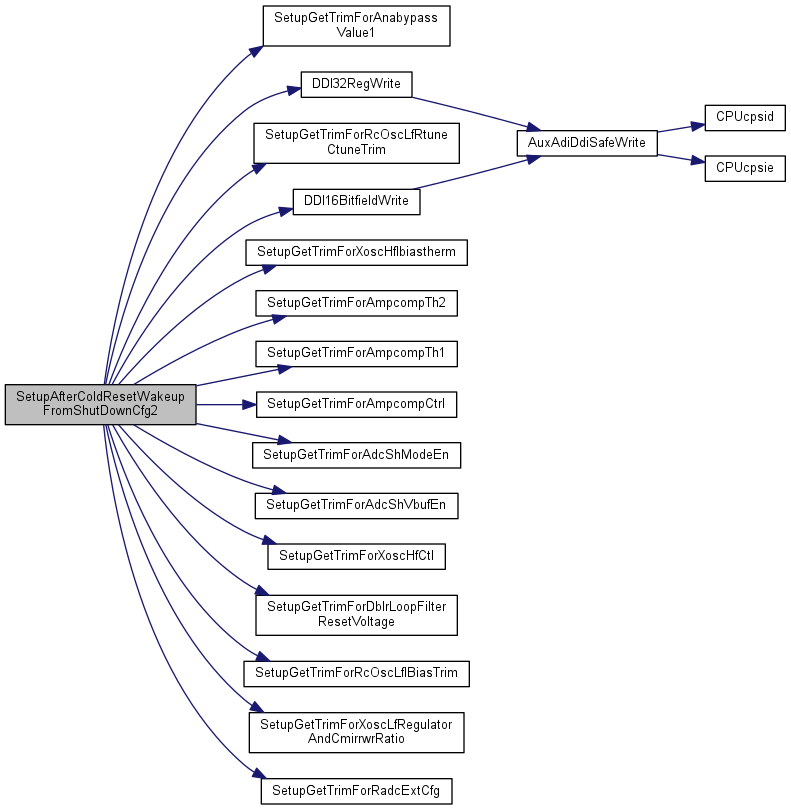
179 {
180  uint32_t ui32Trim;
181 
182  // Following sequence is required for using XOSCHF, if not included
183  // devices crashes when trying to switch to XOSCHF.
184  //
185  // Trim CAP settings. Get and set trim value for the ANABYPASS_VALUE1
186  // register
187  ui32Trim = SetupGetTrimForAnabypassValue1( ccfg_ModeConfReg );
189 
190  // Trim RCOSC_LF. Get and set trim values for the RCOSCLF_RTUNE_TRIM and
191  // RCOSCLF_CTUNE_TRIM fields in the XOSCLF_RCOSCLF_CTRL register.
197  ui32Trim);
198 
199  // Trim XOSCHF IBIAS THERM. Get and set trim value for the
200  // XOSCHF IBIAS THERM bit field in the ANABYPASS_VALUE2 register. Other
201  // register bit fields are set to 0.
202  ui32Trim = SetupGetTrimForXoscHfIbiastherm();
205 
206  // Trim AMPCOMP settings required before switch to XOSCHF
207  ui32Trim = SetupGetTrimForAmpcompTh2();
209  ui32Trim = SetupGetTrimForAmpcompTh1();
211 #if ( CCFG_BASE == CCFG_BASE_DEFAULT )
212  ui32Trim = SetupGetTrimForAmpcompCtrl( ui32Fcfg1Revision );
213 #else
214  ui32Trim = NOROM_SetupGetTrimForAmpcompCtrl( ui32Fcfg1Revision );
215 #endif
217 
218  // Set trim for DDI_0_OSC_ADCDOUBLERNANOAMPCTL_ADC_SH_MODE_EN in accordance to FCFG1 setting
219  // This is bit[5] in the DDI_0_OSC_O_ADCDOUBLERNANOAMPCTL register
220  // Using MASK4 write + 1 => writing to bits[7:4]
221  ui32Trim = SetupGetTrimForAdcShModeEn( ui32Fcfg1Revision );
222  HWREGB( AUX_DDI0_OSC_BASE + DDI_O_MASK4B + ( DDI_0_OSC_O_ADCDOUBLERNANOAMPCTL * 2 ) + 1 ) =
223  ( 0x20 | ( ui32Trim << 1 ));
224 
225  // Set trim for DDI_0_OSC_ADCDOUBLERNANOAMPCTL_ADC_SH_VBUF_EN in accordance to FCFG1 setting
226  // This is bit[4] in the DDI_0_OSC_O_ADCDOUBLERNANOAMPCTL register
227  // Using MASK4 write + 1 => writing to bits[7:4]
228  ui32Trim = SetupGetTrimForAdcShVbufEn( ui32Fcfg1Revision );
229  HWREGB( AUX_DDI0_OSC_BASE + DDI_O_MASK4B + ( DDI_0_OSC_O_ADCDOUBLERNANOAMPCTL * 2 ) + 1 ) =
230  ( 0x10 | ( ui32Trim ));
231 
232  // Set trim for the PEAK_DET_ITRIM, HP_BUF_ITRIM and LP_BUF_ITRIM bit fields
233  // in the DDI0_OSC_O_XOSCHFCTL register in accordance to FCFG1 setting.
234  // Remaining register bit fields are set to their reset values of 0.
235  ui32Trim = SetupGetTrimForXoscHfCtl(ui32Fcfg1Revision);
237 
238  // Set trim for DBLR_LOOP_FILTER_RESET_VOLTAGE in accordance to FCFG1 setting
239  // (This is bits [18:17] in DDI_0_OSC_O_ADCDOUBLERNANOAMPCTL)
240  // (Using MASK4 write + 4 => writing to bits[19:16] => (4*4))
241  // (Assuming: DDI_0_OSC_ADCDOUBLERNANOAMPCTL_DBLR_LOOP_FILTER_RESET_VOLTAGE_S = 17 and
242  // that DDI_0_OSC_ADCDOUBLERNANOAMPCTL_DBLR_LOOP_FILTER_RESET_VOLTAGE_M = 0x00060000)
243  ui32Trim = SetupGetTrimForDblrLoopFilterResetVoltage( ui32Fcfg1Revision );
244  HWREGB( AUX_DDI0_OSC_BASE + DDI_O_MASK4B + ( DDI_0_OSC_O_ADCDOUBLERNANOAMPCTL * 2 ) + 4 ) =
245  ( 0x60 | ( ui32Trim << 1 ));
246 
247  // Update DDI_0_OSC_ATESTCTL_ATESTLF_RCOSCLF_IBIAS_TRIM with data from
249  // This is DDI_0_OSC_O_ATESTCTL bit[7]
250  // ( DDI_0_OSC_O_ATESTCTL is currently hidden (but=0x00000020))
251  // Using MASK4 write + 1 => writing to bits[7:4]
252  ui32Trim = SetupGetTrimForRcOscLfIBiasTrim( ui32Fcfg1Revision );
253  HWREGB( AUX_DDI0_OSC_BASE + DDI_O_MASK4B + ( 0x00000020 * 2 ) + 1 ) =
254  ( 0x80 | ( ui32Trim << 3 ));
255 
258  // This can be simplified since the registers are packed together in the same
259  // order both in FCFG1 and in the HW register.
260  // This spans DDI_0_OSC_O_LFOSCCTL bits[23:18]
261  // Using MASK8 write + 4 => writing to bits[23:16]
262  ui32Trim = SetupGetTrimForXoscLfRegulatorAndCmirrwrRatio( ui32Fcfg1Revision );
263  HWREGH( AUX_DDI0_OSC_BASE + DDI_O_MASK8B + ( DDI_0_OSC_O_LFOSCCTL * 2 ) + 4 ) =
264  ( 0xFC00 | ( ui32Trim << 2 ));
265 
266  // Set trim the HPM_IBIAS_WAIT_CNT, LPM_IBIAS_WAIT_CNT and IDAC_STEP bit
267  // fields in the DDI0_OSC_O_RADCEXTCFG register in accordance to FCFG1 setting.
268  // Remaining register bit fields are set to their reset values of 0.
269  ui32Trim = SetupGetTrimForRadcExtCfg(ui32Fcfg1Revision);
271 
272  // Setting FORCE_KICKSTART_EN (ref. CC26_V1_BUG00261). Should also be done for PG2
273  // (This is bit 22 in DDI_0_OSC_O_CTL0)
275 }
uint32_t SetupGetTrimForAmpcompTh1(void)
Returns the trim value to be used for the AMPCOMP_TH1 register in OSC_DIG.
Definition: setup_rom.c:556
uint32_t SetupGetTrimForRcOscLfRtuneCtuneTrim(void)
Returns the trim value to be used for the RCOSCLF_RTUNE_TRIM and the RCOSCLF_CTUNE_TRIM bit fields in...
Definition: setup_rom.c:473
uint32_t SetupGetTrimForAmpcompTh2(void)
Returns the trim value to be used for the AMPCOMP_TH2 register in OSC_DIG.
Definition: setup_rom.c:521
uint32_t SetupGetTrimForDblrLoopFilterResetVoltage(uint32_t ui32Fcfg1Revision)
Returns the trim value from FCFG1 to be used as DBLR_LOOP_FILTER_RESET_VOLTAGE setting.
Definition: setup_rom.c:673
uint32_t SetupGetTrimForAdcShVbufEn(uint32_t ui32Fcfg1Revision)
Returns the trim value from FCFG1 to be used as ADC_SH_VBUF_EN setting.
Definition: setup_rom.c:711
void DDI16BitfieldWrite(uint32_t ui32Base, uint32_t ui32Reg, uint32_t ui32Mask, uint32_t ui32Shift, uint16_t ui32Data)
Write a bitfield via the DDI using 16-bit maskable write.
Definition: ddi.c:117
uint32_t SetupGetTrimForRadcExtCfg(uint32_t ui32Fcfg1Revision)
Returns the trim value to be used for the RADCEXTCFG register in OSC_DIG.
Definition: setup_rom.c:780
uint32_t SetupGetTrimForRcOscLfIBiasTrim(uint32_t ui32Fcfg1Revision)
Returns the FCFG1 OSC_CONF_ATESTLF_RCOSCLF_IBIAS_TRIM.
Definition: setup_rom.c:812
uint32_t SetupGetTrimForXoscLfRegulatorAndCmirrwrRatio(uint32_t ui32Fcfg1Revision)
Returns XOSCLF_REGULATOR_TRIM and XOSCLF_CMIRRWR_RATIO as one packet spanning bits [5:0] in the retur...
Definition: setup_rom.c:832
uint32_t SetupGetTrimForAnabypassValue1(uint32_t ccfg_ModeConfReg)
Returns the trim value to be used for the ANABYPASS_VALUE1 register in OSC_DIG.
Definition: setup_rom.c:403
uint32_t SetupGetTrimForAdcShModeEn(uint32_t ui32Fcfg1Revision)
Returns the trim value from FCFG1 to be used as ADC_SH_MODE_EN setting.
Definition: setup_rom.c:692
uint32_t SetupGetTrimForAmpcompCtrl(uint32_t ui32Fcfg1Revision)
Returns the trim value to be used for the AMPCOMP_CTRL register in OSC_DIG.
Definition: setup_rom.c:591
void DDI32RegWrite(uint32_t ui32Base, uint32_t ui32Reg, uint32_t ui32Val)
Write a 32 bit value to a register in the DDI slave.
Definition: ddi.c:66
uint32_t SetupGetTrimForXoscHfCtl(uint32_t ui32Fcfg1Revision)
Returns the trim value to be used for the XOSCHFCTL register in OSC_DIG.
Definition: setup_rom.c:730
uint32_t SetupGetTrimForXoscHfIbiastherm(void)
Returns the trim value to be used for the XOSC_HF_IBIASTHERM bit field in the ANABYPASS_VALUE2 regist...
Definition: setup_rom.c:501

Here is the call graph for this function:

void SetupAfterColdResetWakeupFromShutDownCfg3 ( uint32_t  ccfg_ModeConfReg)

Third part of configuration required when waking up from shutdown.

Referenced by TrimAfterColdResetWakeupFromShutDown().

284 {
285  uint32_t fcfg1OscConf;
286  uint32_t ui32Trim;
287  uint32_t currentHfClock;
288  uint32_t ccfgExtLfClk;
289 
290  // Examin the XOSC_FREQ field to select 0x1=HPOSC, 0x2=48MHz XOSC, 0x3=24MHz XOSC
291  switch (( ccfg_ModeConfReg & CCFG_MODE_CONF_XOSC_FREQ_M ) >> CCFG_MODE_CONF_XOSC_FREQ_S ) {
292  case 2 :
293  // XOSC source is a 48 MHz xtal
294  // Do nothing (since this is the reset setting)
295  break;
296  case 1 :
297  // XOSC source is HPOSC (trim the HPOSC if this is a chip with HPOSC, otherwise skip trimming and default to 24 MHz XOSC)
298 
299  fcfg1OscConf = HWREG( FCFG1_BASE + FCFG1_O_OSC_CONF );
300 
301  if (( fcfg1OscConf & FCFG1_OSC_CONF_HPOSC_OPTION ) == 0 ) {
302  // This is a HPOSC chip, apply HPOSC settings
303  // Set bit DDI_0_OSC_CTL0_HPOSC_MODE_EN (this is bit 14 in DDI_0_OSC_O_CTL0)
305 
313 
326  break;
327  }
328  // Not a HPOSC chip - fall through to default
329  default :
330  // XOSC source is a 24 MHz xtal (default)
331  // Set bit DDI_0_OSC_CTL0_XTAL_IS_24M (this is bit 31 in DDI_0_OSC_O_CTL0)
333  break;
334  }
335 
336  // Set XOSC_HF in bypass mode if CCFG is configured for external TCXO
337  // Please note that it is up to the custommer to make sure that the external clock source is up and running before XOSC_HF can be used.
340  }
341 
342  // Clear DDI_0_OSC_CTL0_CLK_LOSS_EN (ClockLossEventEnable()). This is bit 9 in DDI_0_OSC_O_CTL0.
343  // This is typically already 0 except on Lizard where it is set in ROM-boot
345 
346  // Setting DDI_0_OSC_CTL1_XOSC_HF_FAST_START according to value found in FCFG1
347  ui32Trim = SetupGetTrimForXoscHfFastStart();
348  HWREGB( AUX_DDI0_OSC_BASE + DDI_O_MASK4B + ( DDI_0_OSC_O_CTL1 * 2 )) = ( 0x30 | ui32Trim );
349 
350  // setup the LF clock based upon CCFG:MODE_CONF:SCLK_LF_OPTION
351  switch (( ccfg_ModeConfReg & CCFG_MODE_CONF_SCLK_LF_OPTION_M ) >> CCFG_MODE_CONF_SCLK_LF_OPTION_S ) {
352  case 0 : // XOSC_HF_DLF (XOSCHF/1536) -> SCLK_LF (=31250Hz)
354  SetupSetAonRtcSubSecInc( 0x8637BD );
355  break;
356  case 1 : // EXTERNAL signal -> SCLK_LF (frequency=2^38/CCFG_EXT_LF_CLK_RTC_INCREMENT)
357  // Set SCLK_LF to use the same source as SCLK_HF
358  // Can be simplified a bit since possible return values for HF matches LF settings
359  currentHfClock = OSCClockSourceGet( OSC_SRC_CLK_HF );
360  OSCClockSourceSet( OSC_SRC_CLK_LF, currentHfClock );
361  while( OSCClockSourceGet( OSC_SRC_CLK_LF ) != currentHfClock ) {
362  // Wait until switched
363  }
364  ccfgExtLfClk = HWREG( CCFG_BASE + CCFG_O_EXT_LF_CLK );
368  IOC_STD_INPUT | IOC_HYST_ENABLE ); // Route external clock to AON IOC w/hysteresis
369  // Set XOSC_LF in bypass mode to allow external 32k clock
371  // Fall through to set XOSC_LF as SCLK_LF source
372  case 2 : // XOSC_LF -> SLCK_LF (32768 Hz)
374  break;
375  default : // (=3) RCOSC_LF
377  break;
378  }
379 
380  // Update ADI_4_AUX_ADCREF1_VTRIM with value from FCFG1
381  HWREGB( AUX_ADI4_BASE + ADI_4_AUX_O_ADCREF1 ) =
386 
387  // Set ADI_4_AUX:ADC0.SMPL_CYCLE_EXP to it's default minimum value (=3)
388  // (Note: Using MASK8B requires that the bits to be modified must be within the same
389  // byte boundary which is the case for the ADI_4_AUX_ADC0_SMPL_CYCLE_EXP field)
390  HWREGH( AUX_ADI4_BASE + ADI_O_MASK8B + ( ADI_4_AUX_O_ADC0 * 2 )) =
392 
393  // Sync with AON
394  SysCtrlAonSync();
395 }
static void SysCtrlAonSync(void)
Sync all accesses to the AON register interface.
Definition: sys_ctrl.h:177
#define IOC_PORT_AON_CLK32K
Definition: ioc.h:169
uint32_t OSCClockSourceGet(uint32_t ui32SrcClk)
Get the source clock settings.
Definition: osc.c:147
#define IOC_STD_INPUT
Definition: ioc.h:296
void SetupSetAonRtcSubSecInc(uint32_t subSecInc)
Doing the tricky stuff needed to enter new RTCSUBSECINC value.
Definition: setup_rom.c:901
#define OSC_SRC_CLK_HF
Definition: osc.h:112
#define OSC_XOSC_HF
Definition: osc.h:117
#define OSC_SRC_CLK_LF
Definition: osc.h:114
#define OSC_RCOSC_LF
Definition: osc.h:118
void IOCPortConfigureSet(uint32_t ui32IOId, uint32_t ui32PortId, uint32_t ui32IOConfig)
Set the configuration of an IO port.
Definition: ioc.c:96
#define IOC_HYST_ENABLE
Definition: ioc.h:220
uint32_t SetupGetTrimForXoscHfFastStart(void)
Returns the trim value to be used as OSC_DIG:CTL1.XOSC_HF_FAST_START.
Definition: setup_rom.c:762
void OSCClockSourceSet(uint32_t ui32SrcClk, uint32_t ui32Osc)
Configure the oscillator input to the a source clock.
Definition: osc.c:100
#define OSC_XOSC_LF
Definition: osc.h:119

Here is the call graph for this function:

uint32_t SetupGetTrimForAdcShModeEn ( uint32_t  ui32Fcfg1Revision)

Returns the trim value from FCFG1 to be used as ADC_SH_MODE_EN setting.

Referenced by SetupAfterColdResetWakeupFromShutDownCfg2().

693 {
694  uint32_t getTrimForAdcShModeEnValue = 1; // Recommended default setting
695 
696  if ( ui32Fcfg1Revision >= 0x00000022 ) {
697  getTrimForAdcShModeEnValue = ( HWREG( FCFG1_BASE + FCFG1_O_OSC_CONF ) &
700  }
701 
702  return ( getTrimForAdcShModeEnValue );
703 }
uint32_t SetupGetTrimForAdcShVbufEn ( uint32_t  ui32Fcfg1Revision)

Returns the trim value from FCFG1 to be used as ADC_SH_VBUF_EN setting.

Referenced by SetupAfterColdResetWakeupFromShutDownCfg2().

712 {
713  uint32_t getTrimForAdcShVbufEnValue = 1; // Recommended default setting
714 
715  if ( ui32Fcfg1Revision >= 0x00000022 ) {
716  getTrimForAdcShVbufEnValue = ( HWREG( FCFG1_BASE + FCFG1_O_OSC_CONF ) &
719  }
720 
721  return ( getTrimForAdcShVbufEnValue );
722 }
uint32_t SetupGetTrimForAmpcompCtrl ( uint32_t  ui32Fcfg1Revision)

Returns the trim value to be used for the AMPCOMP_CTRL register in OSC_DIG.

Referenced by SetupAfterColdResetWakeupFromShutDownCfg2().

592 {
593  uint32_t ui32TrimValue ;
594  uint32_t ui32Fcfg1Value ;
595  uint32_t ibiasOffset ;
596  uint32_t ibiasInit ;
597  uint32_t modeConf1 ;
598  int32_t deltaAdjust ;
599 
600  // Use device specific trim values located in factory configuration
601  // area. Register bit fields without trim values in the factory
602  // configuration area will be set to the value of 0.
603  ui32Fcfg1Value = HWREG( FCFG1_BASE + FCFG1_O_AMPCOMP_CTRL1 );
604 
605  ibiasOffset = ( ui32Fcfg1Value &
608  ibiasInit = ( ui32Fcfg1Value &
611 
613  // Adjust with DELTA_IBIAS_OFFSET and DELTA_IBIAS_INIT from CCFG
614  modeConf1 = HWREG( CCFG_BASE + CCFG_O_MODE_CONF_1 );
615 
616  // Both fields are signed 4-bit values. This is an assumption when doing the sign extension.
617  deltaAdjust =
620  deltaAdjust += (int32_t)ibiasOffset;
621  if ( deltaAdjust < 0 ) {
622  deltaAdjust = 0;
623  }
626  }
627  ibiasOffset = (uint32_t)deltaAdjust;
628 
629  deltaAdjust =
630  (((int32_t)( modeConf1 << ( 32 - CCFG_MODE_CONF_1_DELTA_IBIAS_INIT_W - CCFG_MODE_CONF_1_DELTA_IBIAS_INIT_S )))
632  deltaAdjust += (int32_t)ibiasInit;
633  if ( deltaAdjust < 0 ) {
634  deltaAdjust = 0;
635  }
638  }
639  ibiasInit = (uint32_t)deltaAdjust;
640  }
641  ui32TrimValue = ( ibiasOffset << DDI_0_OSC_AMPCOMPCTL_IBIAS_OFFSET_S ) |
642  ( ibiasInit << DDI_0_OSC_AMPCOMPCTL_IBIAS_INIT_S ) ;
643 
644  ui32TrimValue |= (((ui32Fcfg1Value &
648  ui32TrimValue |= (((ui32Fcfg1Value &
652  ui32TrimValue |= (((ui32Fcfg1Value &
656 
657  if ( ui32Fcfg1Revision >= 0x00000022 ) {
658  ui32TrimValue |= ((( ui32Fcfg1Value &
662  }
663 
664  return(ui32TrimValue);
665 }
uint32_t SetupGetTrimForAmpcompTh1 ( void  )

Returns the trim value to be used for the AMPCOMP_TH1 register in OSC_DIG.

Referenced by SetupAfterColdResetWakeupFromShutDownCfg2().

557 {
558  uint32_t ui32TrimValue;
559  uint32_t ui32Fcfg1Value;
560 
561  // Use device specific trim values located in factory configuration
562  // area. All defined register bit fields have a corresponding trim
563  // value in the factory configuration area
564  ui32Fcfg1Value = HWREG(FCFG1_BASE + FCFG1_O_AMPCOMP_TH1);
565  ui32TrimValue = (((ui32Fcfg1Value &
569  ui32TrimValue |= (((ui32Fcfg1Value &
573  ui32TrimValue |= (((ui32Fcfg1Value &
577  ui32TrimValue |= (((ui32Fcfg1Value &
581 
582  return(ui32TrimValue);
583 }
uint32_t SetupGetTrimForAmpcompTh2 ( void  )

Returns the trim value to be used for the AMPCOMP_TH2 register in OSC_DIG.

Referenced by SetupAfterColdResetWakeupFromShutDownCfg2().

522 {
523  uint32_t ui32TrimValue;
524  uint32_t ui32Fcfg1Value;
525 
526  // Use device specific trim value located in factory configuration
527  // area. All defined register bit fields have corresponding trim
528  // value in the factory configuration area
529  ui32Fcfg1Value = HWREG(FCFG1_BASE + FCFG1_O_AMPCOMP_TH2);
530  ui32TrimValue = ((ui32Fcfg1Value &
534  ui32TrimValue |= (((ui32Fcfg1Value &
538  ui32TrimValue |= (((ui32Fcfg1Value &
542  ui32TrimValue |= (((ui32Fcfg1Value &
546 
547  return(ui32TrimValue);
548 }
uint32_t SetupGetTrimForAnabypassValue1 ( uint32_t  ccfg_ModeConfReg)

Returns the trim value to be used for the ANABYPASS_VALUE1 register in OSC_DIG.

Referenced by SetupAfterColdResetWakeupFromShutDownCfg2().

404 {
405  uint32_t ui32Fcfg1Value ;
406  uint32_t ui32XoscHfRow ;
407  uint32_t ui32XoscHfCol ;
408  uint32_t ui32TrimValue ;
409 
410  // Use device specific trim values located in factory configuration
411  // area for the XOSC_HF_COLUMN_Q12 and XOSC_HF_ROW_Q12 bit fields in
412  // the ANABYPASS_VALUE1 register. Value for the other bit fields
413  // are set to 0.
414 
415  ui32Fcfg1Value = HWREG(FCFG1_BASE + FCFG1_O_CONFIG_OSC_TOP);
416  ui32XoscHfRow = (( ui32Fcfg1Value &
419  ui32XoscHfCol = (( ui32Fcfg1Value &
422 
423  if (( ccfg_ModeConfReg & CCFG_MODE_CONF_XOSC_CAP_MOD ) == 0 ) {
424  // XOSC_CAP_MOD = 0 means: CAP_ARRAY_DELTA is in use -> Apply compensation
425  // XOSC_CAPARRAY_DELTA is located in bit[15:8] of ccfg_ModeConfReg
426  // Note: HW_REV_DEPENDENT_IMPLEMENTATION. Field width is not given by
427  // a define and sign extension must therefore be hardcoded.
428  // ( A small test program is created verifying the code lines below:
429  // Ref.: ..\test\small_standalone_test_programs\CapArrayDeltaAdjust_test.c)
430  int32_t i32CustomerDeltaAdjust =
431  (((int32_t)( ccfg_ModeConfReg << ( 32 - CCFG_MODE_CONF_XOSC_CAPARRAY_DELTA_W - CCFG_MODE_CONF_XOSC_CAPARRAY_DELTA_S )))
433 
434  while ( i32CustomerDeltaAdjust < 0 ) {
435  ui32XoscHfCol >>= 1; // COL 1 step down
436  if ( ui32XoscHfCol == 0 ) { // if COL below minimum
437  ui32XoscHfCol = 0xFFFF; // Set COL to maximum
438  ui32XoscHfRow >>= 1; // ROW 1 step down
439  if ( ui32XoscHfRow == 0 ) { // if ROW below minimum
440  ui32XoscHfRow = 1; // Set both ROW and COL
441  ui32XoscHfCol = 1; // to minimum
442  }
443  }
444  i32CustomerDeltaAdjust++;
445  }
446  while ( i32CustomerDeltaAdjust > 0 ) {
447  ui32XoscHfCol = ( ui32XoscHfCol << 1 ) | 1; // COL 1 step up
448  if ( ui32XoscHfCol > 0xFFFF ) { // if COL above maximum
449  ui32XoscHfCol = 1; // Set COL to minimum
450  ui32XoscHfRow = ( ui32XoscHfRow << 1 ) | 1; // ROW 1 step up
451  if ( ui32XoscHfRow > 0xF ) { // if ROW above maximum
452  ui32XoscHfRow = 0xF; // Set both ROW and COL
453  ui32XoscHfCol = 0xFFFF; // to maximum
454  }
455  }
456  i32CustomerDeltaAdjust--;
457  }
458  }
459 
460  ui32TrimValue = (( ui32XoscHfRow << DDI_0_OSC_ANABYPASSVAL1_XOSC_HF_ROW_Q12_S ) |
461  ( ui32XoscHfCol << DDI_0_OSC_ANABYPASSVAL1_XOSC_HF_COLUMN_Q12_S ) );
462 
463  return (ui32TrimValue);
464 }
uint32_t SetupGetTrimForDblrLoopFilterResetVoltage ( uint32_t  ui32Fcfg1Revision)

Returns the trim value from FCFG1 to be used as DBLR_LOOP_FILTER_RESET_VOLTAGE setting.

Referenced by SetupAfterColdResetWakeupFromShutDownCfg2().

674 {
675  uint32_t dblrLoopFilterResetVoltageValue = 0; // Reset value
676 
677  if ( ui32Fcfg1Revision >= 0x00000020 ) {
678  dblrLoopFilterResetVoltageValue = ( HWREG( FCFG1_BASE + FCFG1_O_MISC_OTP_DATA_1 ) &
681  }
682 
683  return ( dblrLoopFilterResetVoltageValue );
684 }
uint32_t SetupGetTrimForRadcExtCfg ( uint32_t  ui32Fcfg1Revision)

Returns the trim value to be used for the RADCEXTCFG register in OSC_DIG.

Referenced by SetupAfterColdResetWakeupFromShutDownCfg2().

781 {
782  uint32_t getTrimForRadcExtCfgValue = 0x403F8000; // Recommended default setting
783  uint32_t fcfg1Data;
784 
785  if ( ui32Fcfg1Revision >= 0x00000020 ) {
786  fcfg1Data = HWREG( FCFG1_BASE + FCFG1_O_MISC_OTP_DATA_1 );
787  getTrimForRadcExtCfgValue =
788  ( ( ( fcfg1Data & FCFG1_MISC_OTP_DATA_1_HPM_IBIAS_WAIT_CNT_M ) >>
791 
792  getTrimForRadcExtCfgValue |=
793  ( ( ( fcfg1Data & FCFG1_MISC_OTP_DATA_1_LPM_IBIAS_WAIT_CNT_M ) >>
796 
797  getTrimForRadcExtCfgValue |=
798  ( ( ( fcfg1Data & FCFG1_MISC_OTP_DATA_1_IDAC_STEP_M ) >>
801  }
802 
803  return ( getTrimForRadcExtCfgValue );
804 }
uint32_t SetupGetTrimForRcOscLfIBiasTrim ( uint32_t  ui32Fcfg1Revision)

Returns the FCFG1 OSC_CONF_ATESTLF_RCOSCLF_IBIAS_TRIM.

Referenced by SetupAfterColdResetWakeupFromShutDownCfg2().

813 {
814  uint32_t trimForRcOscLfIBiasTrimValue = 0; // Default value
815 
816  if ( ui32Fcfg1Revision >= 0x00000022 ) {
817  trimForRcOscLfIBiasTrimValue = ( HWREG( FCFG1_BASE + FCFG1_O_OSC_CONF ) &
820  }
821 
822  return ( trimForRcOscLfIBiasTrimValue );
823 }
uint32_t SetupGetTrimForRcOscLfRtuneCtuneTrim ( void  )

Returns the trim value to be used for the RCOSCLF_RTUNE_TRIM and the RCOSCLF_CTUNE_TRIM bit fields in the XOSCLF_RCOSCLF_CTRL register in OSC_DIG.

Referenced by SetupAfterColdResetWakeupFromShutDownCfg2().

474 {
475  uint32_t ui32TrimValue;
476 
477  // Use device specific trim values located in factory configuration
478  // area
479  ui32TrimValue =
484 
485  ui32TrimValue |=
490 
491  return(ui32TrimValue);
492 }
uint32_t SetupGetTrimForXoscHfCtl ( uint32_t  ui32Fcfg1Revision)

Returns the trim value to be used for the XOSCHFCTL register in OSC_DIG.

Referenced by SetupAfterColdResetWakeupFromShutDownCfg2().

731 {
732  uint32_t getTrimForXoschfCtlValue = 0; // Recommended default setting
733  uint32_t fcfg1Data;
734 
735  if ( ui32Fcfg1Revision >= 0x00000020 ) {
736  fcfg1Data = HWREG( FCFG1_BASE + FCFG1_O_MISC_OTP_DATA_1 );
737  getTrimForXoschfCtlValue =
738  ( ( ( fcfg1Data & FCFG1_MISC_OTP_DATA_1_PEAK_DET_ITRIM_M ) >>
741 
742  getTrimForXoschfCtlValue |=
743  ( ( ( fcfg1Data & FCFG1_MISC_OTP_DATA_1_HP_BUF_ITRIM_M ) >>
746 
747  getTrimForXoschfCtlValue |=
748  ( ( ( fcfg1Data & FCFG1_MISC_OTP_DATA_1_LP_BUF_ITRIM_M ) >>
751  }
752 
753  return ( getTrimForXoschfCtlValue );
754 }
uint32_t SetupGetTrimForXoscHfFastStart ( void  )

Returns the trim value to be used as OSC_DIG:CTL1.XOSC_HF_FAST_START.

Referenced by SetupAfterColdResetWakeupFromShutDownCfg3().

763 {
764  uint32_t ui32XoscHfFastStartValue ;
765 
766  // Get value from FCFG1
767  ui32XoscHfFastStartValue = ( HWREG( FCFG1_BASE + FCFG1_O_OSC_CONF ) &
770 
771  return ( ui32XoscHfFastStartValue );
772 }
uint32_t SetupGetTrimForXoscHfIbiastherm ( void  )

Returns the trim value to be used for the XOSC_HF_IBIASTHERM bit field in the ANABYPASS_VALUE2 register in OSC_DIG.

Referenced by SetupAfterColdResetWakeupFromShutDownCfg2().

502 {
503  uint32_t ui32TrimValue;
504 
505  // Use device specific trim value located in factory configuration
506  // area
507  ui32TrimValue =
511 
512  return(ui32TrimValue);
513 }
uint32_t SetupGetTrimForXoscLfRegulatorAndCmirrwrRatio ( uint32_t  ui32Fcfg1Revision)

Returns XOSCLF_REGULATOR_TRIM and XOSCLF_CMIRRWR_RATIO as one packet spanning bits [5:0] in the returned value.

Referenced by SetupAfterColdResetWakeupFromShutDownCfg2().

833 {
834  uint32_t trimForXoscLfRegulatorAndCmirrwrRatioValue = 0; // Default value for both fields
835 
836  if ( ui32Fcfg1Revision >= 0x00000022 ) {
837  trimForXoscLfRegulatorAndCmirrwrRatioValue = ( HWREG( FCFG1_BASE + FCFG1_O_OSC_CONF ) &
841  }
842 
843  return ( trimForXoscLfRegulatorAndCmirrwrRatioValue );
844 }
void SetupSetAonRtcSubSecInc ( uint32_t  subSecInc)

Doing the tricky stuff needed to enter new RTCSUBSECINC value.

Returns
None

Referenced by SetupAfterColdResetWakeupFromShutDownCfg3().

902 {
903  // Loading a new RTCSUBSECINC value is done in 5 steps:
904  // 1. Write bit[15:0] of new SUBSECINC value to AUX_WUC_O_RTCSUBSECINC0
905  // 2. Write bit[23:16] of new SUBSECINC value to AUX_WUC_O_RTCSUBSECINC1
907  // 4. Wait for AUX_WUC_RTCSUBSECINCCTL_UPD_ACK
910  HWREG( AUX_WUC_BASE + AUX_WUC_O_RTCSUBSECINC1 ) = (( subSecInc >> 16 ) & AUX_WUC_RTCSUBSECINC1_INC23_16_M );
911 
915 }
void SetupSetCacheModeAccordingToCcfgSetting ( void  )

Set correct VIMS_MODE according to CCFG setting (CACHE or GPRAM)

Returns
None

Referenced by SetupTrimDevice().

855 {
856  // - Make sure to enable aggressive VIMS clock gating for power optimization
857  // Only for PG2 devices.
858  // - Enable cache prefetch enable as default setting
859  // (Slightly higher power consumption, but higher CPU performance)
860  // - IF ( CCFG_..._DIS_GPRAM == 1 )
861  // then: Enable cache (set cache mode = 1), even if set by ROM boot code
862  // (This is done because it's not set by boot code when running inside
863  // a debugger supporting the Halt In Boot (HIB) functionality).
864  // else: Set MODE_GPRAM if not already set (see inline comments as well)
865  uint32_t vimsCtlMode0 ;
866 
867  while ( HWREGBITW( VIMS_BASE + VIMS_O_STAT, VIMS_STAT_MODE_CHANGING_BITN )) {
868  // Do nothing - wait for an eventual ongoing mode change to complete.
869  // (There should typically be no wait time here, but need to be sure)
870  }
871 
872  // Note that Mode=0 is equal to MODE_GPRAM
873  vimsCtlMode0 = (( HWREG( VIMS_BASE + VIMS_O_CTL ) & ~VIMS_CTL_MODE_M ) | VIMS_CTL_DYN_CG_EN_M | VIMS_CTL_PREF_EN_M );
874 
875 
877  // Enable cache (and hence disable GPRAM)
878  HWREG( VIMS_BASE + VIMS_O_CTL ) = ( vimsCtlMode0 | VIMS_CTL_MODE_CACHE );
879  } else if (( HWREG( VIMS_BASE + VIMS_O_STAT ) & VIMS_STAT_MODE_M ) != VIMS_STAT_MODE_GPRAM ) {
880  // GPRAM is enabled in CCFG but not selected
881  // Note: It is recommended to go via MODE_OFF when switching to MODE_GPRAM
882  HWREG( VIMS_BASE + VIMS_O_CTL ) = ( vimsCtlMode0 | VIMS_CTL_MODE_OFF );
883  while (( HWREG( VIMS_BASE + VIMS_O_STAT ) & VIMS_STAT_MODE_M ) != VIMS_STAT_MODE_OFF ) {
884  // Do nothing - wait for an eventual mode change to complete (This goes fast).
885  }
886  HWREG( VIMS_BASE + VIMS_O_CTL ) = vimsCtlMode0;
887  } else {
888  // Correct mode, but make sure PREF_EN and DYN_CG_EN always are set
889  HWREG( VIMS_BASE + VIMS_O_CTL ) = vimsCtlMode0;
890  }
891 }
static int32_t SetupSignExtendVddrTrimValue ( uint32_t  ui32VddrTrimVal)
inlinestatic

Sign extend the VDDR_TRIM setting (special format ranging from -10 to +21)

Returns

Referenced by SetupAfterColdResetWakeupFromShutDownCfg1(), and SysCtrlSetRechargeBeforePowerDown().

233 {
234  // The VDDR trim value is 5 bits representing the range from -10 to +21
235  // (where -10=0x16, -1=0x1F, 0=0x00, 1=0x01 and +21=0x15)
236  int32_t i32SignedVddrVal = ui32VddrTrimVal;
237  if ( i32SignedVddrVal > 0x15 ) {
238  i32SignedVddrVal -= 0x20;
239  }
240  return ( i32SignedVddrVal );
241 }
void SetupTrimDevice ( void  )

Performs the necessary trim of the device which is not done in boot code.

This function should only execute coming from ROM boot. The current implementation does not take soft reset into account. However, it does no damage to execute it again. It only consumes time.
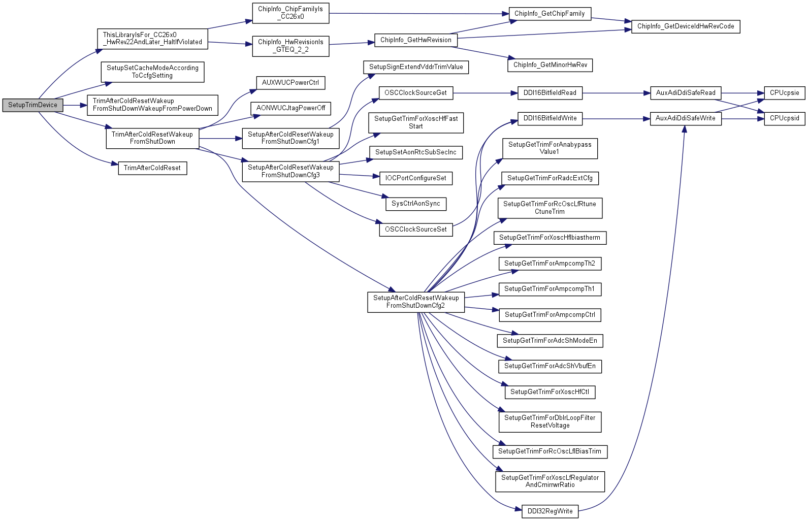
Returns
None
113 {
114  uint32_t ui32Fcfg1Revision;
115  uint32_t ui32AonSysResetctl;
116 
117  // Get layout revision of the factory configuration area
118  // (Handle undefined revision as revision = 0)
119  ui32Fcfg1Revision = HWREG(FCFG1_BASE + FCFG1_O_FCFG1_REVISION);
120  if ( ui32Fcfg1Revision == 0xFFFFFFFF ) {
121  ui32Fcfg1Revision = 0;
122  }
123 
124  // This driverlib version and setup file is for CC26x0 PG2.2 and later
125  // Halt if violated
127 
128  // Enable standby in flash bank
130 
131  // Clock must always be enabled for the semaphore module (due to ADI/DDI HW workaround)
133 
134  // Warm resets on CC13x0 and CC26x0 complicates software design because much of
135  // our software expect that initialization is done from a full system reset.
136  // This includes RTC setup, oscillator configuration and AUX setup.
137  // To ensure a full reset of the device is done when customers get e.g. a Watchdog
138  // reset, the following is set here:
140 
141  // Select correct CACHE mode and set correct CACHE configuration
142 #if ( CCFG_BASE == CCFG_BASE_DEFAULT )
144 #else
145  NOROM_SetupSetCacheModeAccordingToCcfgSetting();
146 #endif
147 
148  // 1. Check for powerdown
149  // 2. Check for shutdown
150  // 3. Assume cold reset if none of the above.
151  //
152  // It is always assumed that the application will freeze the latches in
153  // AON_IOC when going to powerdown in order to retain the values on the IOs.
154  //
155  // NB. If this bit is not cleared before proceeding to powerdown, the IOs
156  // will all default to the reset configuration when restarting.
158  {
159  // NB. This should be calling a ROM implementation of required trim and
160  // compensation
161  // e.g. TrimAfterColdResetWakeupFromShutDownWakeupFromPowerDown()
163  }
164  // Check for shutdown
165  //
166  // When device is going to shutdown the hardware will automatically clear
167  // the SLEEPDIS bit in the SLEEP register in the AON_SYSCTL module.
168  // It is left for the application to assert this bit when waking back up,
169  // but not before the desired IO configuration has been re-established.
171  {
172  // NB. This should be calling a ROM implementation of required trim and
173  // compensation
174  // e.g. TrimAfterColdResetWakeupFromShutDown() -->
175  // TrimAfterColdResetWakeupFromShutDownWakeupFromPowerDown();
176  TrimAfterColdResetWakeupFromShutDown(ui32Fcfg1Revision);
178  }
179  else
180  {
181  // Consider adding a check for soft reset to allow debugging to skip
182  // this section!!!
183  //
184  // NB. This should be calling a ROM implementation of required trim and
185  // compensation
186  // e.g. TrimAfterColdReset() -->
187  // TrimAfterColdResetWakeupFromShutDown() -->
188  // TrimAfterColdResetWakeupFromShutDownWakeupFromPowerDown()
190  TrimAfterColdResetWakeupFromShutDown(ui32Fcfg1Revision);
192 
193  }
194 
195  // Set VIMS power domain control.
196  // PDCTL1VIMS = 0 ==> VIMS power domain is only powered when CPU power domain is powered
197  HWREG( PRCM_BASE + PRCM_O_PDCTL1VIMS ) = 0;
198 
199  // Configure optimal wait time for flash FSM in cases where flash pump
200  // wakes up from sleep
201  HWREG(FLASH_BASE + FLASH_O_FPAC1) = (HWREG(FLASH_BASE + FLASH_O_FPAC1) &
203  (0x139<<FLASH_FPAC1_PSLEEPTDIS_S);
204 
205  // And finally at the end of the flash boot process:
206  // SET BOOT_DET bits in AON_SYSCTL to 3 if already found to be 1
207  // Note: The BOOT_DET_x_CLR/SET bits must be manually cleared
208  if ((( HWREG( AON_SYSCTL_BASE + AON_SYSCTL_O_RESETCTL ) &
211  {
212  ui32AonSysResetctl = ( HWREG( AON_SYSCTL_BASE + AON_SYSCTL_O_RESETCTL ) &
216  HWREG( AON_SYSCTL_BASE + AON_SYSCTL_O_RESETCTL ) = ui32AonSysResetctl;
217  }
218 
219  // Make sure there are no ongoing VIMS mode change when leaving SetupTrimDevice()
220  // (There should typically be no wait time here, but need to be sure)
221  while ( HWREGBITW( VIMS_BASE + VIMS_O_STAT, VIMS_STAT_MODE_CHANGING_BITN )) {
222  // Do nothing - wait for an eventual ongoing mode change to complete.
223  }
224 }
static void TrimAfterColdResetWakeupFromShutDownWakeupFromPowerDown(void)
Trims to be applied when coming from POWER_DOWN (also called when coming from SHUTDOWN and PIN_RESET)...
Definition: setup.c:235
void SetupSetCacheModeAccordingToCcfgSetting(void)
Set correct VIMS_MODE according to CCFG setting (CACHE or GPRAM)
Definition: setup_rom.c:854
static void TrimAfterColdResetWakeupFromShutDown(uint32_t ui32Fcfg1Revision)
Trims to be applied when coming from SHUTDOWN (also called when coming from PIN_RESET).
Definition: setup.c:249
static void TrimAfterColdReset(void)
Trims to be applied when coming from PIN_RESET.
Definition: setup.c:357
void ThisLibraryIsFor_CC26x0_HwRev22AndLater_HaltIfViolated(void)
Verifies that current chip is CC26x0 HwRev 2.2 or later and never returns if violated.
Definition: chipinfo.c:200

Here is the call graph for this function: