|
AM263x MCU+ SDK
08.03.01
|


|
|
AM263x MCU+ SDK
08.03.01
|
|
ControlCard
LaunchPad
| DAC Instance | HSEC PIN |
|---|---|
| DAC | 9 (ADC1_MUX_SEL signal LOW) |
| ADC Instance | ADC channel | HSEC PIN |
|---|---|---|
| ADC0 | ADC0_AIN0 | 9 (ADC1_MUX_SEL signal HIGH) |
| ADC0 | ADC0_AIN1 | 11 (ADC1_MUX_SEL signal HIGH) |
| ADC0 | ADC0_AIN2 | 15 |
| ADC0 | ADC0_AIN3 | 17 |
| ADC0 | ADC0_AIN4 | 21 |
| ADC0 | ADC0_AIN5 | 23 |
| ADC1 | ADC1_AIN0 | 12 |
| ADC1 | ADC1_AIN1 | 14 |
| ADC1 | ADC1_AIN2 | 18 |
| ADC1 | ADC1_AIN3 | 20 |
| ADC1 | ADC1_AIN4 | 24 |
| ADC1 | ADC1_AIN5 | 26 |
| ADC2 | ADC2_AIN0 | 31 |
| ADC2 | ADC2_AIN1 | 33 |
| ADC2 | ADC2_AIN2 | 37 |
| ADC2 | ADC2_AIN3 | 39 |
| ADC2 | ADC2_AIN4 | - |
| ADC2 | ADC2_AIN5 | - |
| ADC3 | ADC3_AIN0 | 28 |
| ADC3 | ADC3_AIN1 | 30 |
| ADC3 | ADC3_AIN2 | 34 |
| ADC3 | ADC3_AIN3 | 36 |
| ADC3 | ADC3_AIN4 | 40 |
| ADC3 | ADC3_AIN5 | 42 |
| ADC4 | ADC4_AIN0 | 25 (ADC2_MUX_SEL signal HIGH) |
| ADC4 | ADC4_AIN1 | 27 (ADC2_MUX_SEL signal HIGH) |
| ADC4 | ADC4_AIN2 | - |
| ADC4 | ADC4_AIN3 | - |
| ADC4 | ADC4_AIN4 | - |
| ADC4 | ADC4_AIN5 | - |
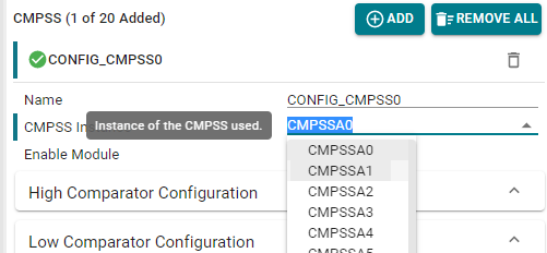
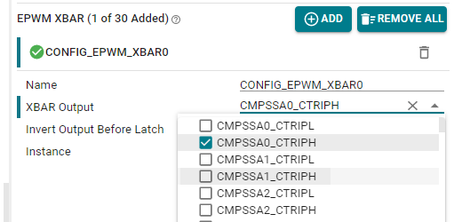
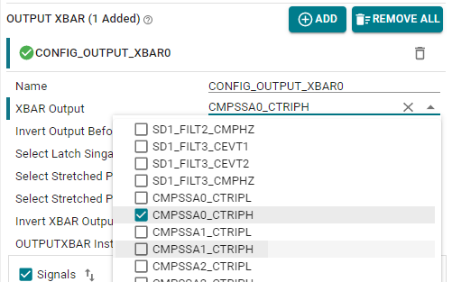
A CMPSS example that enables the CMPSS High comparator and feeds the asynchronous output to GPIO and EPWM
This example enables the CMPSSA0 CMPSSA1 COMPH comparator and feeds the asynchronous CTRIPOUTH signal to the XBAROUT0 pin and CTRIPH to EPWM0B.
CMPSS is configured to generate trip signals to trip the EPWM signals. CMPIN1P is used to give positive input and internal DAC is configured to provide the negative input. Internal DAC is configured to provide a signal at VDD/2. An EPWM signal is generated at EPWM0B and is configured to be tripped by CTRIPOUTH.
When a low input(VSS) is provided to CMPIN1P,
When a high input(higher than VDD/2) is provided to CMPIN1P,
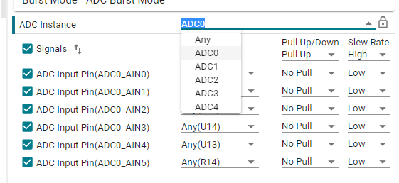
This example sets up ePWM0 to periodically trigger a set of conversions (SOC0,1,12,13,14,15) on ADC0 ADC1 for conversion of inputs on ADC_AIN0, ADC_AIN1 and burst mode conversion on ADC_AIN3.
This demonstrates a batch of conversion on ADC0 ADC1 (inputs on ADC_AIN0 and ADC_AIN1) and burst mode conversion on ADC0 ADC1 (input ADC_AIN3)
ADC0 ADC1 Interrupt ISR is used to read results of ADC0 ADC1 (i.e. digital representations of inputs ADC_AIN0, ADC_AIN1 and average of oversampled ADC_AIN3)
The below watch variables can be used to view ADC conversion results.
Watch Variables gAdc0Result0 - Digital representation of the voltage on pin ADC0_AIN0 ADC1_AIN0 gAdc0result1 - Digital representation of the voltage on pin ADC0_AIN1 ADC1_AIN1 gadc0Result2 - Digital representation of the voltage on pin ADC0_AIN3 ADC1_AIN3
ADC0_AIN0 ADC1_AIN0, ADC0_AIN1 ADC1_AIN1, ADC0_AIN3 ADC1_AIN3 pins should be connected to signals to be converted.
Check example.syscfg


This example sets up ePWM0 to periodically trigger a set of conversions (SOC0,1) on ADC0 ADC1 for conversion of inputs on ADC_AIN0, ADC_AIN1 in differential modes (ADC_AIN0 - ADC_AIN1) on SOC0 and (ADC_AIN1 - ADC_AIN0) on SOC1. Note: In differential mode, the outputs are symmetric across "2112 or 0x840" i.e., if there is a 1v on differential input, expected output should be around 2752 or 0xAC0. if there is a -1v on differential input, expected output should be around 1472 or 0x5C0. Expect overflow if the readings are above 4224 ADC0 ADC1 Interrupt ISR is used to read results of ADC0 ADC1 (i.e. digital representations of inputs ADC_AIN0, ADC_AIN1 and average of oversampled ADC_AIN3) The below watch variables can be used to view ADC conversion results. Watch Variables gAdc0Result0 - Digital representation of the differential voltage on pins ADC0_AIN0 - ADC0_AIN1 ADC1_AIN0 - ADC1_AIN1 gAdc0result1 - Digital representation of the differential voltage on pins ADC0_AIN1 - ADC0_AIN0 ADC1_AIN1 - ADC1_AIN0 External Connections ADC0_AIN0 ADC1_AIN0, ADC0_AIN1 ADC1_AIN1 pins should be connected to signals to be converted. Check example.syscfg
This example sets up ePWM0 to periodically trigger a set of conversions (SOC0,1,2) on ADC0 ADC2 and ADC1. This demonstrates multiple ADCs working together to process a batch of conversions using the available parallelism across multiple ADCs. ADC0 ADC2 Interrupt ISR is used to read results of both ADC0 ADC2 and ADC1. The below watch variables can be used to view ADC conversion results. External Connections ADC0_AIN0 ADC2_AIN0, ADC0_AIN1 ADC2_AIN1, ADC0_AIN2 ADC2_AIN2 and ADC1_AIN0, ADC1_AIN1, ADC1_AIN2 pins should be connected to signals to be converted. Watch Variables gAdc0Result0 - Digital representation of the voltage on pin ADC0_AIN0 ADC2_AIN0 gAdc0result1 - Digital representation of the voltage on pin ADC0_AIN1 ADC2_AIN1 adc0Result2 - Digital representation of the voltage on pin ADC0_AIN2 ADC2_AIN2 adc1Result0 - Digital representation of the voltage on pin ADC1_AIN0 adc1Result1 - Digital representation of the voltage on pin ADC1_AIN1 adc1Result2 - Digital representation of the voltage on pin ADC1_AIN2

This example uses the ADC Post Processing Block to trip a ePWM in case of out of bound input.
ADCINT1 is configured to periodically trigger the ADC. Initially ADC is triggered through software.
Limit detection Post processing block is configured and if ADC results are outside the defined range, the PPB will generate an ADCxEVTy event. This signal is configured as trip source for EPWM0, 1 and 2.
This example showcases one-shot, cycle-by-cycle and direct tripping of PWMs.
External Connections ADC0_AIN2 ADC1_AIN2 pin should be connected to DAC output pin. EPWM0A, EPWM0B, EPWM1A, EPWM1B, EPWM2A, EPWM2B can be connected to an oscilloscope to validate tripping.
Watch Variables adc0Result2 - Digital representation of the voltage on pin ADC0_AIN2 ADC1_AIN2

This example sets up two ADC channels to convert simultaneously. The results will be transferred by DMA into a buffer in RAM.
It configures ePWM0 to trigger SOC0 on ADC0 ADC2 and ADC1. EPWM is only used to trigger the first ADC conversion. INT0 of ADC0 ADC2 is configured to generate interrupt after first conversion and will then disable EPWM SOC generation. INT1 of both ADC's is configured to enable continuous conversion.
DMA channel 0 is triggered at EOC0 of ADC0 ADC2 and will copy conversion result to a buffer in RAM. DMA channel 1 is triggered at EOC0 of ADC1 and will copy conversion result to another buffer in RAM. DMA will generate interrupt after the buffer is filled and will stop conversion on both ADC's.
The below watch variables can be used to view ADC conversion results.
External Connections ADC0_AIN0 ADC2_AIN0 and ADC1_AIN0 pins should be connected to signals to be converted.
Watch Variables gAdc0DataBuffer - Buffers which stores conversion results from ADC0 gAdc1DataBuffer - Buffers which stores conversion results from ADC1


This example uses the ADC module to perform an ADC SOC conversion triggered by software.
In this example ADC0 ADC1 is used to convert the SOC, the user can also select a different one.
This example also showcases how to configure and use the ADC module.

 1.8.20