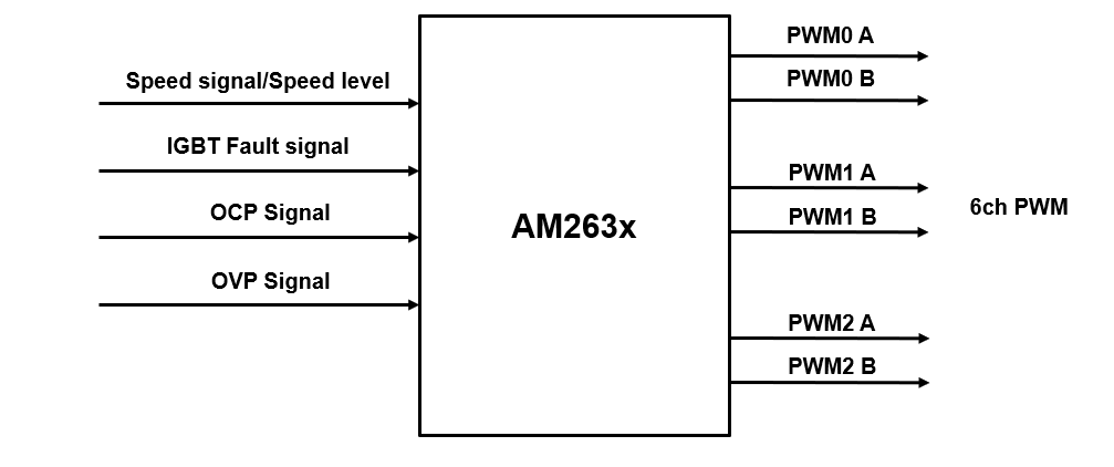
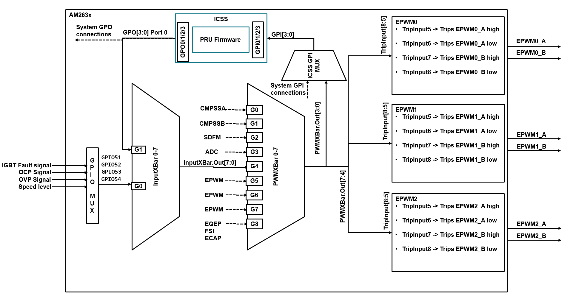
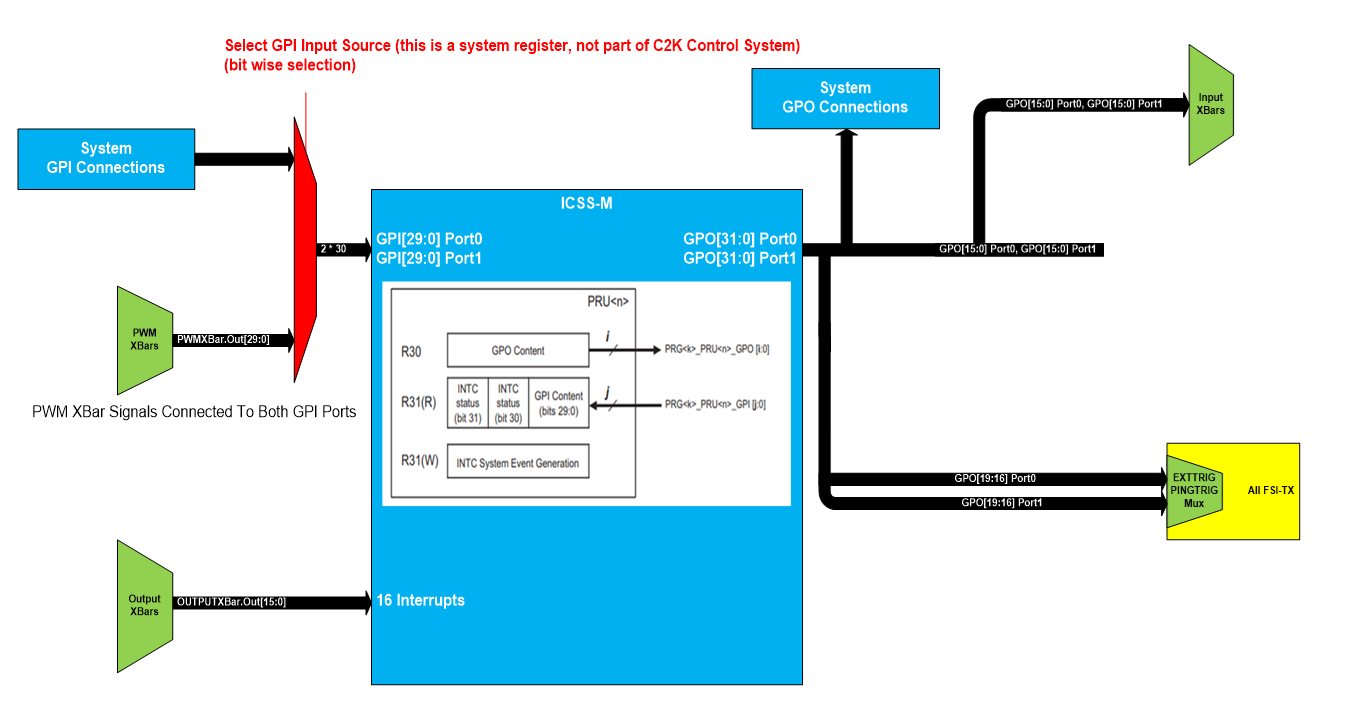
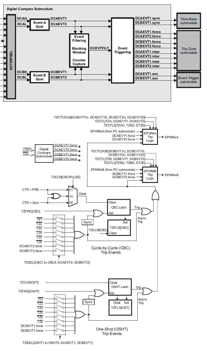
Signal path: GPIO51/52/53/54 -> INPUTXBAR0/1/2/3 -> PWMXBAR0/1/2/3 -> GPI0/1/2/3 ICSS (PRU firmware reads GPI reg, process, writes to GPO reg) GPO0/1/2/3 -> INPUTXBAR4/5/6/7 -> PWMXBAR4/5/6/7 -> EPWM0+1+2 Trip5/6/7/8
.retain ; Required for building .out with assembly file
.retainrefs ; Required for building .out with assembly file
.global main
.sect ".text"
.asg r31, gpi_reg
.asg r30, gpo_reg
.asg r1.b0, offset_reg8
.asg r20, temp_reg32
.asg r21.b0, input_bits_reg8
.asg r22.b0, trip_bits_reg8
.asg r23.b0, clr_reg8
.asg r24.b0, zero_reg8
.asg r25, freewheeling_countdown_reg32
.asg r26, freewheeling_time_reg32
.asg 0, LUT_OFFSET ; 16 byte. Offset of Look up table for PRU FW use. Placed at base of PRU DMEM0 - as optimization
; Initialize before PRU FW load and run
.asg 16, PROTECTION_STATUS_OFFSET ; 1 byte. Offset of Protection status from PRU
.asg 20, PROTECTION_STATUS_CLR_OFFSET ; 1 byte. Offset of Clear request from R5
.asg 24, PRU_FW_VERSION_OFFSET ; 4 byte. Offset of PRU firmware version
.asg 28, FREEWHEELING_TIME_OFFSET ; 4 byte. Offset of Freewheeling time
; Initialize before PRU FW load and run
main:
;Initializations
ldi gpo_reg.b0, 0x00 ;Clear GPO and GPI registers
ldi gpi_reg.b0, 0x00
ldi zero_reg8, 0 ;Initialize constant value registers
ldi offset_reg8, PRU_FW_VERSION_OFFSET
ldi temp_reg32.w0, 0x0002 ;Write firmware version. Version 2
ldi temp_reg32.w2, 0x0000
sbco &temp_reg32, c24, offset_reg8, 4
ldi offset_reg8, FREEWHEELING_TIME_OFFSET ;Initialization of freewheeling time
lbco &freewheeling_countdown_reg32, c24, offset_reg8, 4
poll_gpi:
;Wait for fault
mov input_bits_reg8, gpi_reg.b0 ;1 cycle. Latch input bits
qbeq poll_gpi, input_bits_reg8, 0 ;1 cycle. Poll inputs until non zero. Optimization: Remove this and directly look up. This will reduce latency to enter protection status, but reduces frequency of polling
lbco &trip_bits_reg8, c24, input_bits_reg8, 1 ;3 cycle. Look up in LUT at DMEM0. Optimization: move to PRU core registers
qbeq poll_gpi, trip_bits_reg8, 0 ;1 cycle. Continue to poll if no protection required
;Freewheeling
qbeq end_freewheeling, freewheeling_countdown_reg32, 0 ;1 cycle. Skip freewheeling if no or 0 freewheeling time
ldi gpo_reg.b0, 0x0a ;1 cycle. Turn off all PWMs
freewheeling: ; Freewheeling start.
sub freewheeling_countdown_reg32, freewheeling_countdown_reg32, 1 ; 1 cycle * freewheeling time programmed
qbne freewheeling, freewheeling_countdown_reg32, 0 ; 1 cycle * freewheeling time programmed
end_freewheeling:
;Apply protection and notify CPU
mov gpo_reg.b0, trip_bits_reg8 ;1 cycle. Apply trip output signals to GPO
sbco &trip_bits_reg8, c24, PROTECTION_STATUS_OFFSET, 1 ;2 cycle. Write trip bits as protection status
;Wait for clear command from CPU and clear
poll_clr:
lbco &clr_reg8, c24, PROTECTION_STATUS_CLR_OFFSET, 1 ;3 cycles
qbeq poll_clr, clr_reg8, 0 ;1 cycle. Poll for clear/ack request from R5F
ldi gpo_reg.b0, 0x00 ;1 cycle. Clear trip output signals to GPO
sbco &zero_reg8, c24, PROTECTION_STATUS_OFFSET, 1 ;2 cycle. Clear protection status
sbco &zero_reg8, c24, PROTECTION_STATUS_CLR_OFFSET, 1 ;2 cycle. Clear clear/ack request
ldi offset_reg8, FREEWHEELING_TIME_OFFSET ;1 cycle. Re-Initialization of freewheeling time
lbco &freewheeling_countdown_reg32, c24, offset_reg8, 4 ;3 cycle.
qba poll_gpi ;1 cycle
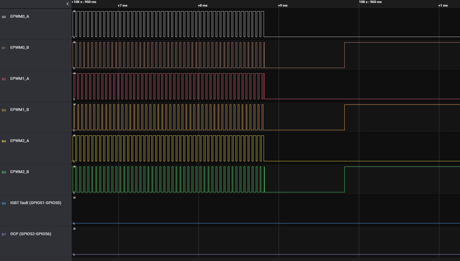
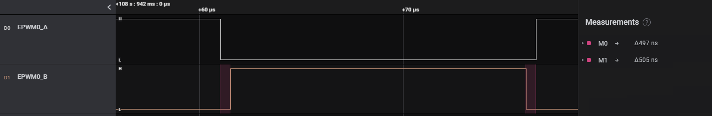
Execution time - from detection of input fault signal to generation of trip output signal : 8 cycles * 5ns. 40ns
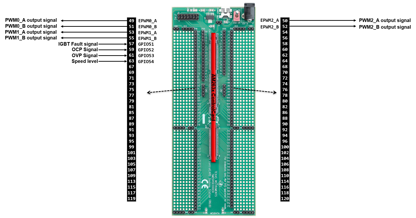
Connect AM263x ControlCard to TMDSHSECDOCK (HSEC180 controlCARD Baseboard Docking Station)
[Cortex_R5_0] EPWM Protection PRU Test Started ...
PRU0 Processor disabled ...
PRU0 IRAM written ...
PRU LUT written ...
Freewheeling time written ...
PRU0 Processor enabled ...
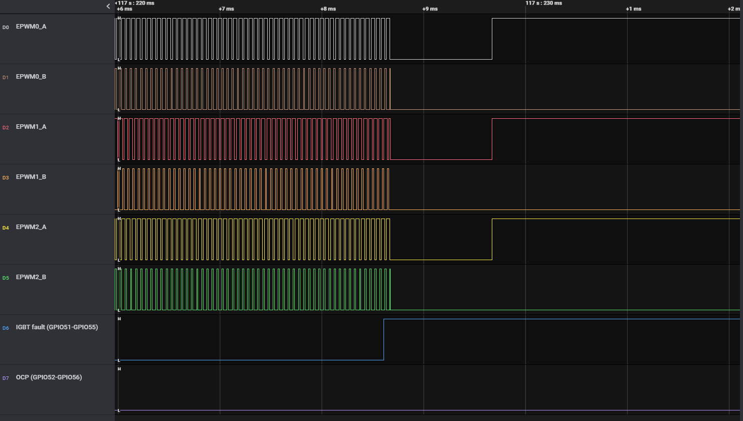
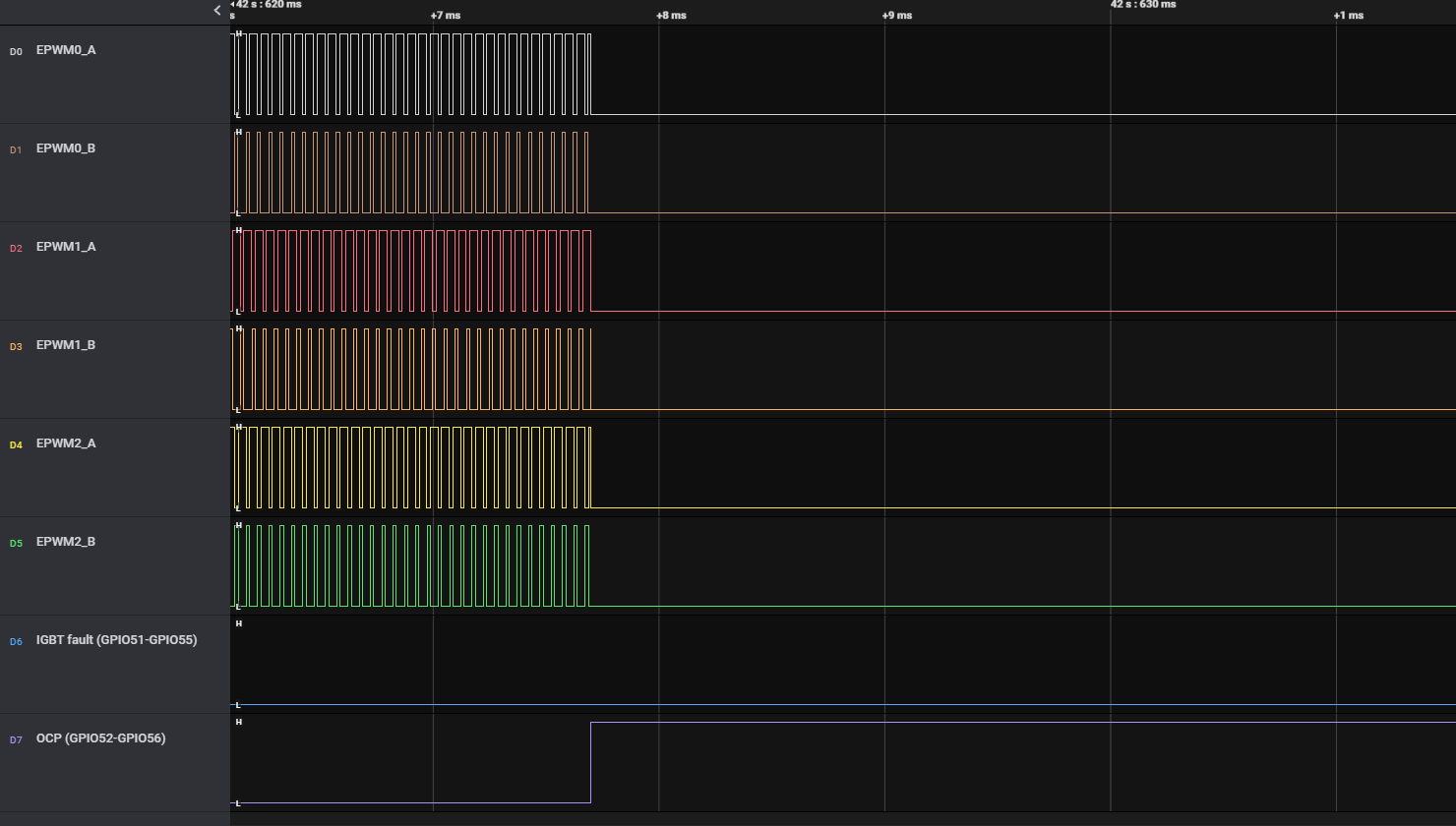
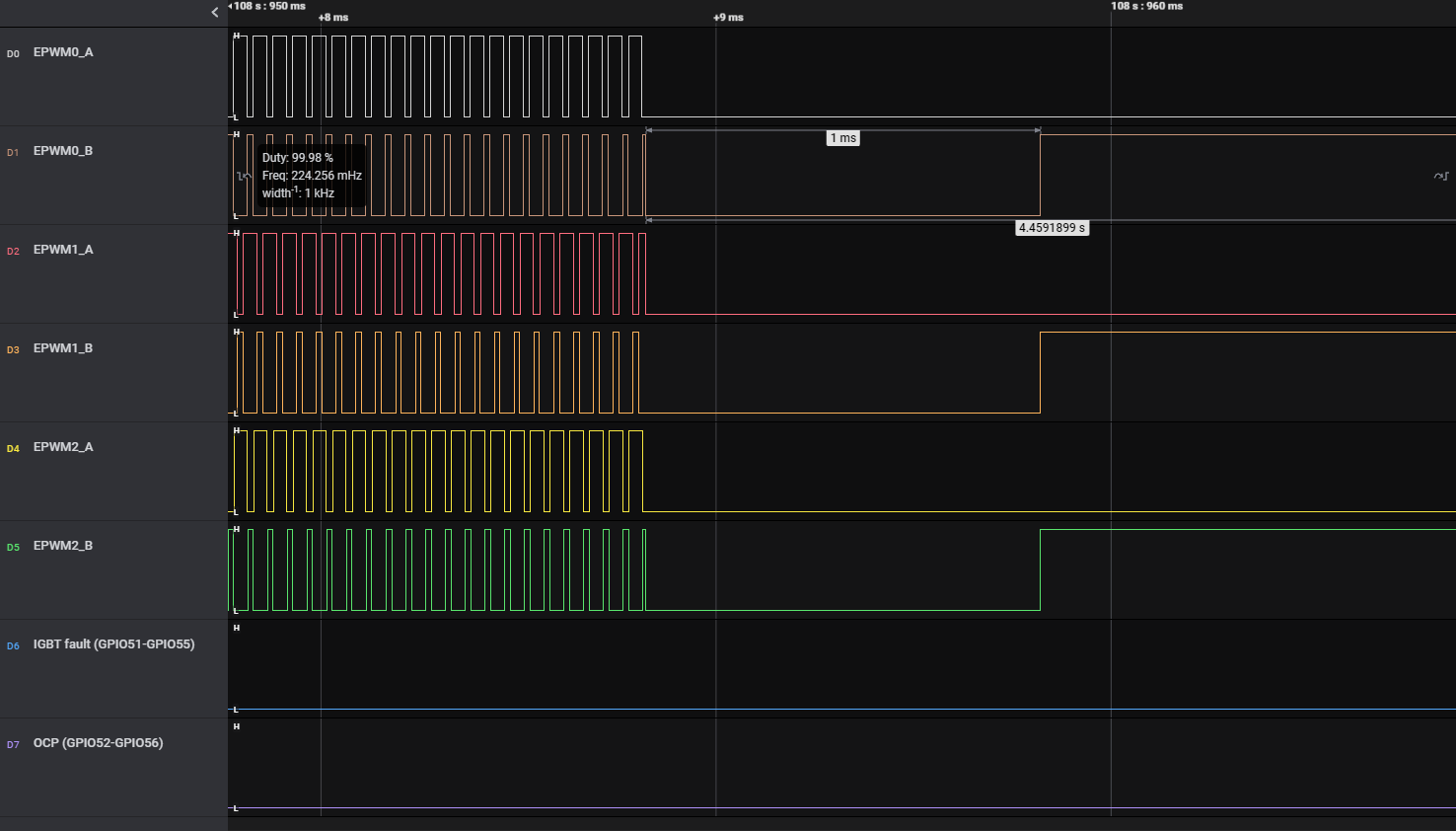
Normal PWM output (check PWM0_A, PWM0_B, PWM1_A, PWM1_B, PWM2_A, PWM2_B)...
Generating test signals (IGBT fault, OCP, OVP, Speed level signals)...
OCP set.
Done...
Waiting to enter protection status...
Waiting to enter protection status...
Entered Protection status 0x0a...
Clearing protection status...
Waiting to clear protection status...
Cleared protection status...
Normal PWM output (check PWM0_A, PWM0_B, PWM1_A, PWM1_B, PWM2_A, PWM2_B)...
Generating test signals (IGBT fault, OCP, OVP, Speed level signals)...
OCP set. IGBT fault set.
Done...
Waiting to enter protection status...
Waiting to enter protection status...
Entered Protection status 0x0a...
Clearing protection status...
Waiting to clear protection status...
Cleared protection status...
Normal PWM output (check PWM0_A, PWM0_B, PWM1_A, PWM1_B, PWM2_A, PWM2_B)...
Generating test signals (IGBT fault, OCP, OVP, Speed level signals)...
OVP set.
Done...
Waiting to enter protection status...
Waiting to enter protection status...
Entered Protection status 0x0a...
Clearing protection status...
Waiting to clear protection status...
Cleared protection status...
Normal PWM output (check PWM0_A, PWM0_B, PWM1_A, PWM1_B, PWM2_A, PWM2_B)...
Generating test signals (IGBT fault, OCP, OVP, Speed level signals)...
OVP set. IGBT fault set.
Done...
Waiting to enter protection status...
Waiting to enter protection status...
Entered Protection status 0x0a...
Clearing protection status...
Waiting to clear protection status...
Cleared protection status...
Normal PWM output (check PWM0_A, PWM0_B, PWM1_A, PWM1_B, PWM2_A, PWM2_B)...
Generating test signals (IGBT fault, OCP, OVP, Speed level signals)...
OCP set. OVP set.
Done...
Waiting to enter protection status...
Waiting to enter protection status...
Entered Protection status 0x0a...
Clearing protection status...
Waiting to clear protection status...
Cleared protection status...
Normal PWM output (check PWM0_A, PWM0_B, PWM1_A, PWM1_B, PWM2_A, PWM2_B)...
Generating test signals (IGBT fault, OCP, OVP, Speed level signals)...
OCP set. OVP set. IGBT fault set.
Done...
Waiting to enter protection status...
Waiting to enter protection status...
Entered Protection status 0x0a...
Clearing protection status...
Waiting to clear protection status...
Cleared protection status...
Normal PWM output (check PWM0_A, PWM0_B, PWM1_A, PWM1_B, PWM2_A, PWM2_B)...
Generating test signals (IGBT fault, OCP, OVP, Speed level signals)...
Speed level set. OCP set.
Done...
Waiting to enter protection status...
Waiting to enter protection status...
Entered Protection status 0x0a...
Clearing protection status...
Waiting to clear protection status...
Cleared protection status...
Normal PWM output (check PWM0_A, PWM0_B, PWM1_A, PWM1_B, PWM2_A, PWM2_B)...
Generating test signals (IGBT fault, OCP, OVP, Speed level signals)...
Speed level set. OCP set. IGBT fault set.
Done...
Waiting to enter protection status...
Waiting to enter protection status...
Entered Protection status 0x0a...
Clearing protection status...
Waiting to clear protection status...
Cleared protection status...
Normal PWM output (check PWM0_A, PWM0_B, PWM1_A, PWM1_B, PWM2_A, PWM2_B)...
Generating test signals (IGBT fault, OCP, OVP, Speed level signals)...
Speed level set. OVP set.
Done...
Waiting to enter protection status...
Waiting to enter protection status...
Entered Protection status 0x06...
Clearing protection status...
Waiting to clear protection status...
Cleared protection status...
Normal PWM output (check PWM0_A, PWM0_B, PWM1_A, PWM1_B, PWM2_A, PWM2_B)...
Generating test signals (IGBT fault, OCP, OVP, Speed level signals)...
Speed level set. IGBT fault set. OVP set.
Done...
Waiting to enter protection status...
Waiting to enter protection status...
Entered Protection status 0x09...
Clearing protection status...
Waiting to clear protection status...
Cleared protection status...
Normal PWM output (check PWM0_A, PWM0_B, PWM1_A, PWM1_B, PWM2_A, PWM2_B)...
Generating test signals (IGBT fault, OCP, OVP, Speed level signals)...
Speed level set. OVP set. OCP set.
Done...
Waiting to enter protection status...
Waiting to enter protection status...
Entered Protection status 0x06...
Clearing protection status...
Waiting to clear protection status...
Cleared protection status...
Normal PWM output (check PWM0_A, PWM0_B, PWM1_A, PWM1_B, PWM2_A, PWM2_B)...
Generating test signals (IGBT fault, OCP, OVP, Speed level signals)...
Speed level set. IGBT fault set. OVP set. OCP set.
Done...
Waiting to enter protection status...
Waiting to enter protection status...
Entered Protection status 0x09...
Clearing protection status...
Waiting to clear protection status...
Cleared protection status...
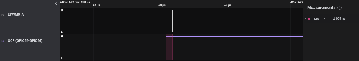
This is the latency of following path: GPIO52 (receives OCP rising edge) -> INPUTXBAR1 -> PWMXBAR1 -> GPI1 ICSS (PRU firmware reads GPI reg, process, writes to GPO reg) GPO0/1/2/3 (0101) -> INPUTXBAR4/5/6/7 -> PWMXBAR4/5/6/7 -> EPWM0+1+2 Trip5/6/7/8 -> PWM0/1/2 A/B(Falling edge)


 1.8.20