Introduction
This example uses DMA to generate a sine wave on the DAC output.
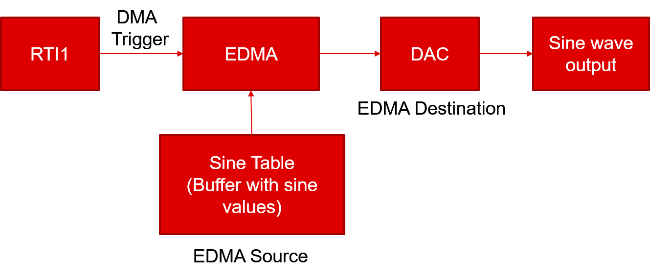
Module Block diagram
The example does the below
- Configures Timer to generate DMA trigger at a rate of 20KHz.
- Calculates sine values and stores it in a buffer (sine table).
- Uses DMA to transfer sine values stored in the sine table to DAC.
- This repeated programming of the DAC registers generates a sine wave.
- The generated output can be viewed throug an oscilloscope on the DAC output pin.
External Connections
- DAC output pin can be connected to an oscilloscope to view the sine wave output.
AM263X-CC
Note: To use the reference voltage generated on ControlCard, make sure that the System VREF source select switch SW8 on ControlCard is set to position 1-2
When using AM263x-CC with TMDSHSECDOCK (HSEC180 controlCARD Baseboard Docking Station)
- Capture waveform on HSEC Pin 9
AM263X-LP
Supported Combinations
| Parameter | Value |
| CPU + OS | r5fss0-0 nortos |
| Toolchain | ti-arm-clang |
| Board | am263x-cc |
| Example folder | examples/drivers/dac/dac_sine_dma/ |
Steps to Run the Example
- When using CCS projects to build, import the CCS project for the required combination and build it using the CCS project menu (see Using SDK with CCS Projects).
- When using makefiles to build, note the required combination and build using make command (see Using SDK with Makefiles)
- Establish connections as mentioned in External Connections section
- Launch a CCS debug session and run the executable, see CCS Launch, Load and Run
- Use an Oscilloscope to view the sine wave on DAC output pin.
See Also
DAC
Sample Output
Shown below is a sample output when the application is run,
DAC Sine DMA Test Started ...
DAC Sine DMA Test Passed!!
All tests have passed!!


 1.8.20