Introduction
This example demonstrates EPWM tripping through ADC limit detection PPB block. ADC0INT1 is configured to periodically trigger the ADC0 channel 2 post initial software forced trigger. The limit detection post-processing block(PPB) is configured and if the ADC results are outside of the defined range, the post-processing block will generate an ADCxEVTy event. This event is configured as EPWM trip source through configuring EPWM XBAR and corresponding EPWM’s trip zone and digital compare sub-modules. The example showcases one-shot, cycle-by-cycle and direct tripping of PWMs through ADCAEVT1 source via Digital compare submodule. DAC is configured to generate a ramp waveform and its output is connected as ADC input. PWM tripping is validated by reading different trip flags.
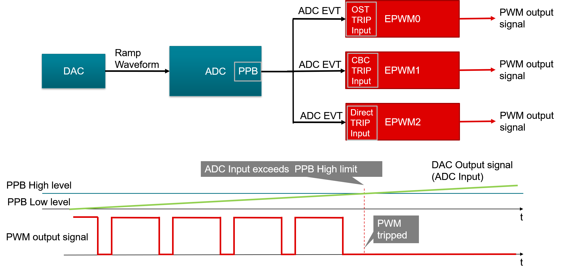
Module Block diagram
The example does the below
- Configures SOC0 of ADC0 to read from Channel 2 and ADC0INT1 to periodically trigger conversions after the initial software forced trigger.
- ADC PPB is configured to generate ADC EVT1 if ADC results are outside the range.
- ADC Event is configured as EPWM trip source through EPWM XBAR.
- Trip Zone and Digital Compare submodule are configured to enable different trip combinations.
- EPWM0 is configured for One Shot trip.
- EPWM1 is configured for Cycle by Cycle trip.
- EPWM2 is configured for Direct trip via Digital compare submodule.
- The ramp waveform on DAC output is routed to ADC input.
- The watch variables storing ADC conversion outputs can be used to view the results.
Watch Variables
- adc0Result2 - Digital representation of the voltage on pin ADC0_AIN2
External Connections
- ADC0_AIN2 pin should be connected to DAC output pin.
- EPWM0A, EPWM0B, EPWM1A, EPWM1B, EPWM2A, EPWM2B can be connected to an oscilloscope to validate tripping.
AM263X-CC
When using AM263x-CC with TMDSHSECDOCK (HSEC180 controlCARD Baseboard Docking Station)
- Connect HSEC Pin 15 (ADC input) to HSEC Pin 9 (DAC out)
- Capture and analyze waveforms at HSEC Pin 49, HSEC Pin 51, HSEC Pin 53, HSEC Pin 55, HSEC Pin 50, HSEC Pin 52
AM263X-LP
Supported Combinations
| Parameter | Value |
| CPU + OS | r5fss0-0 nortos |
| Toolchain | ti-arm-clang |
| Board | am263x-cc, am263x-lp |
| Example folder | examples/drivers/adc/adc_ppb_epwm_trip/ |
Steps to Run the Example
- When using CCS projects to build, import the CCS project for the required combination and build it using the CCS project menu (see Using SDK with CCS Projects).
- When using makefiles to build, note the required combination and build using make command (see Using SDK with Makefiles)
- Establish connections as mentioned in External Connections section
- Launch a CCS debug session and run the executable, see CCS Launch, Load and Run
- Using the watch variables, view the ADC conversion results.
- Observe 6 EPWM waveforms. After ADC input voltage exceeds the PPB limit, PWMs get tripped.
See Also
ADC
Sample Output
Shown below is a sample output when the application is run,
ADC PPB ePWM Trip Test Started ...
ADC PPB ePWM Trip Test Passed!!
All tests have passed!!


 1.8.20