|
AM263Px MCU+ SDK
09.01.00
|


|
|
AM263Px MCU+ SDK
09.01.00
|
|
High performance microcontrollers differ in architecture from traditional microcontrollers. Following diagram shows the differences.

New application software in automotive industry like networking, zonal etc. that runs on these high-performance microcontrollers, requires more than 1 number of CPU, in range of 2-10, and CPU running at core frequencies of 200MHz to 1GHz.
However, in terms of manufacturing, it requires advanced CMOS process nodes and embedded flash is not possible. Therefore, the architecture of these high performance MCU is such that there is no embedded flash and this is very new architecture for microcontroller market.
However, having an external flash architecture comes with its own advantages such as the cost advantage and is estimated of range 20cents to $2 based on flash size.
The other advantage that this gives is memory scalability i.e. to same port, 8MB flash to 128MB flash or more can be attached.
Although having an external flash provides all these advantages, it also comes with its own challenges which needs to be overcome to make external flash microcontroller flexible and robust enough to be used in variety of use case.
Since external flash is connected to microcontroller via pins via tracks on PCB board, there are some serious challenges. First off, number of pins with which external flash is connected is limited therefore, the data bus width is also limited. This limits the performance of XIP and data transfer between external flash and CPU. However, increasing the data bus bits would translate making use of a greater number of pins which itself is a limited resource. Increasing the clock frequency would increase the complexity of board design. Other than this, communication protocol also has an impact on performance. Hence, performance of external flash is limited by a number of parameters and is generally slower than an embedded flash and this concern needs to be addressed.
To make execution from external flash safe and secure, some additional functionality is required. However, these necessary functions also have an impact on performance.
OptiFlash technology is an ecosystem of patented hardware IP, software tools and drivers which aims to at least overcomes all of the previously described generic challenges.
The following diagram shows the OptiFlash technology ecosystem.

AM263Px is 1st device that comes with OptiFlash technology and is next in series with AM263x (AM263x does not have OptiFlash technology).
Following is a representative diagram of AM263x device which does not have OptiFlash technology.

Here, external flash is communicated over QSPI. Any data read/write is being forwarded to QSPI IP.
Coming text will explain how OptiFlash technology is addressing all the previous concerns and new features that are introduced with it.
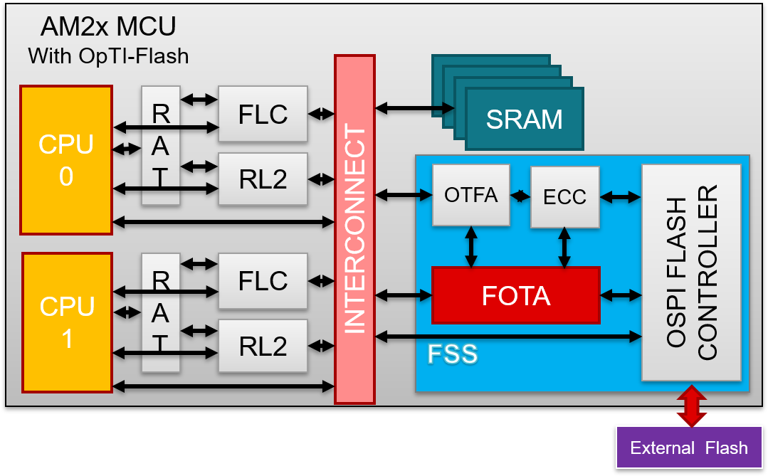
With OptiFlash technology the following hardware blocks has been introduced for XIP performance.

QSPI has been replaced with OSPI or Octal-SPI. The main difference is in the bus width and clock frequency. In AM263Px, OSPI is running at max 133MHz DDR over 8 data lines.
RL2 or remote Layer 2 cache is added. This, basically, is a L2 cache which can be configured to have different size and its cache bank can also be configured to any place in L2 memory.
What this allows is to have a L1 and L2 cache architecture in microcontroller. L1 cache being the CPU cache and L2 being RL2 cache. One point to note is that since external flash only contains read-only data, L2 cache is effectively caching code and rodata only.
FLC or Fast Local Copy is essentially a very simplified DMA but with the ability to allow concurrent execution.
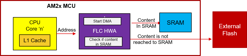
FLC power is in simplicity of programming and Concurrent copy & execution. Only 3 registers are required to be programmed viz. source address, size of transfer and destination address.
Above diagram show the working of FLC. When CPU request an address, if FLC sees that a particular address is copied in the internal SRAM then the data corresponding to that address is returned from SRAM else it is fetched from External Flash. Because the data is returned from internal RAM than external FLASH, fetch time is reduced and this provides some boost in performance.
Although use case of FLC are many, but, from the perspective of system performance improvement, FLC can also be used for implementing overlaying schemes.
Smart placement is a name given to a process, using which functions and other linker-placed objects are distributed across different memories, while accounting for their criticality, directly from the source code with an intention to improve run-time performance. More on this can be read at Smart Placement.
All the above different blocks can be used together to boost the system level performance and the way that can be achieved is
However, step 3 and 4 are optional.
The Logic behind these steps is, suppose, all the functions in a program are in external FLASH and are being XIPed and to improve system performance, it is required to bring a few functions in the internal memory because internal memory is limited. Now the question is what functions are to be brought in the internal memory? Answer to this question is smart placement. Using smart placement, all the performance critical function can be brought in the internal memory which is fast. For few functions, overlay schemes can be used. So all critical function's performance is improved by bringing them in internal memory, however, for rest of the functions which are either not critical or were impossible to be accommodated in the internal memory, then can be accelerated by using L2 cache or RL2.

For safety and security, hardware blocks have been provided. These blocks provide on-the-fly safety and security by splitting up the data in external flash into 32bytes chunk and for each chunk, ECC (Error Correction Code) and MAC (Message Authentication Code) is added as header and footer to that data chunk which is also called metadata.
To enable Safety and Security, all that is required is to enable the hardware. However, it is required to be made sure that the data that is stored in the external flash is also encrypted so as to be read by this safety and security module.
This safety and security module is called ECCM and OTFA.
The way this hardware works is that when CPU requests to fetch an instruction, the entire chunk with its metadata, corresponding to that instruction, is fetched by OSPI controller which is then passed to the ECCM and OTFA hardware which then decrypts and verify data, on-they-fly, and then the instruction is passed on to the CPU to execute.
This allows XIP with full safety and security using hardware accelerators. Using hardware accelerators reduces the impact on performance.
There are many situations, where startup time of any application should be less to achieve system level performance goal. OptiFlash technology brings in some hardware and software features that helps to reduce boot/startup time of an application.
Startup code is usually a code that is badly cached code and even effectiveness of pre-fetch hardware is less. The reason behind this is, startup code always executes once. Other than this, because, startup code would also be calling different function that would be placed all over the memory by the linker in jumbled order. For same reason, performing XIP with L1 and L2 cache enabled (pre-fetch is enabled by default), would not be sufficient.
On software side, order the code layout in memory based on call graph function preorder using metainfo.
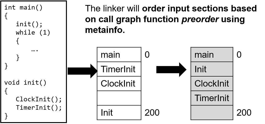
In the above image, before, memory ordering is applied, linker would place different functions in different places based on different parameters. However, with correct ordering, in memory, ClockInit function is placed before TimerInit, because, ClockInit in called before TimerInit.
The above is a very simple example, but, in a real-world, this is more complex. However, this complexity can be handled by compiler/linker.
But by attaining this sort of memory placement which compliments the instruction fetching pattern of CPU of a given type of code, this maximizes usage of pre-fetch hardware.
On the Hardware side, FLC is to be used as it allows simultaneous copy and execution. Before understanding how FLC optimizes boot time, it is important to understand how boot process and bootloader works in MCU+ devices.

Bootloader itself takes some time before it actually starts copying the application. That time it spends by initializing some peripherals, PLLs, etc. or in some complex bootloader, which would integrate entire TCP/IP stack to wait for some message over wire would then be spending some time there as well.
The main idea is that why not to download the application while bootloader is busy somewhere else! However, it is not as straight forward. Let’s say, same idea is rather implemented by DMA, then the problem with this implementation would be that CPU has to wait for DMA to complete copying before CPU can start executing. And this implementation would not work in case where time to download code is more than the time bootloader wait.
This is where FLC comes into picture. FLC allows copying and execution simultaneously. Take the previous case, where, time to copy is more than bootloader wait time.
In context to the above diagram, the way FLC would solve this problem is that for the amount of time bootloader would wait or is busy in performing some other functions, in the background FLC would be copying application startup code. Now when bootloader is finished and switches over the application, CPU would start executing application code. Now for the amount of code that is copied by the FLC, would be returned from faster internal SRAM, rather than being fetched from slower external flash and for rest of the code would be normal XIP. In this manner, boot time of the application can be reduced.

When it comes to high performance MCU which has many cores, using traditional method of compilation is not efficient. Normally, for a microcontroller, compilation goes like the follows:
However, this way of compilation does not scale well. Because if all core's application is using same library, for ex. FreeRTOS or LwIP, etc. then those libraries will be sitting 4 number of times if 4 core's application is using same library.
To address this issue, if all the libraries are placed in a shared memory and then all cores calls these functions from shared memory.
This would change the compilation process to the following:
To enable this sharing of code, OptiFlash technology provides hardware and software tools solution. Software tool is called OptiShare.
During compilation of multi-core project, OptiShare is responsible to identify common code and separation of it from rest of all core's binaries.

However, this way of separating common code does not work standalone. Special hardware needs to be programmed, for this shared code scheme needs to work.
This special hardware that is introduced with OptiFlash technology is called RAT or Region Address Translation.

At run time, this hardware needs to be programmed by the application software before any shared code be called, otherwise, CPU Abort Exceptions will occur.

In typical microcontroller with embedded flash, to be able to perform FOTA, embedded flash size should be more than the double the size of application, because, at a time 2 copy of same application would be stored, in flash. One would be an active application and other would be different version of the application. However, this puts high constraint on embedded flash requirement and this requirement translates to increased BOM cost. Effectively, for an active application, available internal memory is half of total internal memory.
With external flash solution with OptiFlash technology technology, entire internal memory can be used for active image of application. For example, in AM263Px, internal RAM is 3.5MB of total internal memory. An active image of application can use entire internal memory and for new version image of application can be stored in external Flash. Therefore, when looking from typical microcontroller perspective, effective total memory available in AM263Px is alteast 7MB.
However, because OptiFlash technology technology enables XIP, FOTA is difficult to be performed. External flash is connected to microcontroller over 8 data lines (OSPI) and on same data lines, both reads and writes would happen. And in FOTA, writes would be happening while XIP is going on. During writing, reading should be stopped which also mean that XIP needs to be stopped and this would have a huge impact on performance and increased complexity in system design.
Although, FOTA is usually a very low priority task and XIP downtime can be managed in most situation. However, in case, XIP downtime is coming out to be critical, then RWW flash can be used with OptiFlash technology FOTA hardware accelerator.
This role of this accelerator is to schedule reads and writes over same 8 data lines of OSPI. The aim of this hardware is to minimize XIP downtime.
An application has been developed on which XIP performance benchmarks has been done to see how much performance degradation is seen with OptiFlash technology.
The application that is to benchmark performance is an application that would simulate AutoSAR cache miss rate. .text section is in different memories and data in On-Chip RAM. Each test calls 16 separate functions 500 total times in random order. The most instruction intensive example achieves a instruction cache miss rate (ICM/sec) of ~3-4 million per second when run entirely from OCMRAM. This is a rate that we have similarly seen in real-world customer examples.
With Safety and Security Enabled.
| RL2 Cache Size (KB) | Performance Degradation |
|---|---|
| 0KB | 2.36x |
| 8KB | 2.23x |
| 32KB | 1.93x |
| 128KB | 1.10x |
In above table, when Layer 2 cache was disabled, i.e. RL2 is disabled, the above application performed 2.36 times worse than when ran from internal memory. This is when both safety and security is enabled. Now, when L2 cache has been enabled with size of 128KB, the same application performed with just 10% degradation in performance as compared to internal flash.
Below table is without Safety and Security Enabled.
| RL2 Cache Size (KB) | Performance Degradation |
|---|---|
| 0KB | 2.20x |
| 8KB | 1.90x |
| 32KB | 1.73x |
| 128KB | 1.10x |
When on same application, Smart Placement is applied, then 10% boost in performance is seen. More on this can be read at Memory Benchmark with Smart Placement.
 1.8.20