Note
This section is under development
5.1. Board Design Considerations
5.1.1. Introduction
This notes applies to the following devices: • TMS570LSxx and TMS570LC43x • RM4x and RM57Lx
5.1.2. HDK vs Datasheet
In case of any discrepancy between the TI HDKs and the device datasheet, always follow the datasheet. Despite the designer’s best efforts, the HDKs may contain errors which may still function but are not completely aligned with the datasheet specification. Therefore the EVM designs should not be considered as reference designs to be blindly reused.
5.1.3. Clocking Circuit
The Hercules devices offer three options for clock generation: using external crystal, using external oscillator, or feeding the external clock to the EXTCLKIN pin. The frequency of the basic input clock at OSCIN is in the range of 5MHz ~ 20 MHz. The phase lock loop (PLL)is used to multiply the input frequency to some higher frequency.
5.1.3.1. Using Crystal/Resonator as Clock Source
The on-chip oscillator circuit of all the TMS570/RMx devices enables a crystal/resonator connected to the OSCIN and OSCOUT pins. The internal oscillator is a single-stage inverter held in bias by an integrated bias resistor. The crystal is connected across the OSCIN and OSCOUT pins. Kelvin_GND should not be connected to any other GND.
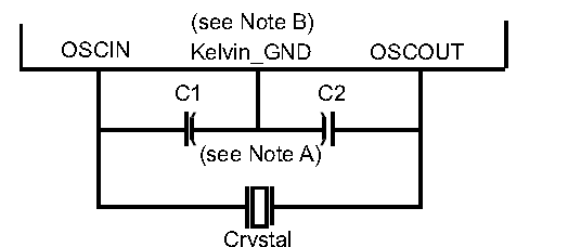
Figure above shows the external circuitry and connections required for using the internal oscillator, along with the equation defining the relationship between the manufacturer’s specified crystal load capacitance CLOAD, formed by two external capacitors C1 and C2. The effective load capacitance, CLOAD, appears to the crystal circuit as the series combination of C1 and C2. Correct CLOAD is important for proper operating frequency. Crystals are available with a variety of CLOAD values.
CLOAD = (C1 * C2 ) / (C1 + C2 ) + CS
CS is the stray capacitance in the oscillator circuit. Stray capacitance is a function of trace lengths, PCB construction, and microcontroller pin design. For a typical design, CS should be approximately 2pF to 4pF. Because C1 and C2 are normally of equal value, the calculation for a typical circuit simplifies slightly to: C1 and C2 = (CLOAD – 3pF) * 2
NOTE: TI strongly encourages each customer to submit samples of the device to the resonator/crystal vendors for validation. The vendors are equipped to determine which load capacitors will best tune their resonator/crystal to the microcontroller device for optimum start-up and operation over temperature and voltage extremes.
5.1.3.2. Using External Oscillator
An external oscillator source can be used by connecting a 3.3-V clock signal to the OSCIN pin and leaving the OSCOUT pin unconnected (open). Kelvin_GND is connected to board digital GND.
5.1.3.3. Using External clock Inputs
The device supports up to two external clock inputs (EXTCLKIN1, EXTCLKIN2). This clock input must be a square-wave input. The maximum clock frequency is 80MHz. The electrical and timing requirements for these clock inputs are specified in device datasheet. The external clock sources are not checked for validity. They are assumed valid when enabled.
5.1.3.4. Oscillator Failure
TMS570 and RMx microcontroller has a built in LPOCLKDET circuitry. The LPOCLKDET (low-power oscillator and clock detect) compares the oscillator input frequency with the internal LPO HF. The clock detect circuit works by checking for a rising edge on one clock (oscillator or HF LPO) between rising edges of the other clock. In case the OSCIN frequency falls out of a frequency window, the CLKDET flags this condition in the global status register (GLBSTAT bit 0: OSC FAIL) and switches all clock domains sourced by OSCIN to the HFLPO clock (limp mode clock). Application firmware should detect the input clock failure and initiate a necessary shut-down procedure for the system.
5.1.3.5. External Clock (ECLK) Output
The ECLK pin can be configured to output a pre-scaled clock signal of the peripheral interface clock (VCLK) frequency. This low-frequency output can be monitored externally as an indicator of the device operating frequency. It also can be used as a clock source for other device. ECLK pin can be configured as a GPIO pin.
5.1.3.6. Crystal Oscillator Circuit Layout
The key layout objectives should be to minimize both the loop area of the oscillator signals and the overall trace length. A poor oscillator layout can result in unreliable or inaccurate oscillator operation and can also be a noise source.
5.1.4. Reset
5.1.4.1. Warm Reset (nRST)
The nRST pin is open-drain bidirectional (input and output) with a glitch filter. The internal circuitry drives the signal low on detecting any device reset condition. An external circuit can assert a device reset by forcing the signal low. On this terminal, the output buffer is implemented as an open drain (drives low only). To ensure an external reset is not arbitrarily generated, TI recommends that an external pullup resistor is connected to this terminal.
The nRST pin has an internal weak pullup. If the open drain reset circuit and its relative switch need a capacitor in order to filter its input signal, an external pullup can speed up the charger of this capacitor.
Caution: Do not connect the nRST pin to a strong high voltage level without a pullup resistor.
The RST pin should never be left floating. It can be driven from a voltage supervisor or other control chip. It can be connected to an external RC combination or it can be pulled up using a 0 to 100K resistor connected to VCCIO (3.3V).
The nRST pin input contains a glitch filter to prevent noise from causing a system reset. It can filter out the pulses less than 475ns (2.1MHz). We still recommend to protect the nRST signal from noise particularly in applications that involve power switching can couple into the reset line. The reset PCB trace should be routed away from noisy signals. Do not run the reset trace close to the edge of the board or parallel to other traces with fast transients.
If the RST signal source is another board, it is recommended to add a buffer IC on the TMS570 board to filter the signal.
A simple push-switch can be used to provide a manual reset. To protect against possible device damage due to electrostatic discharge and to avoid ringing on the nRST signal caused by switch bounce and stray inductance, add a low-value resistor (100 Ω) in series with the switch.
5.1.4.2. Power-On Reset (nPORRST)
This is the power-on reset. This reset must be asserted by an external circuitry whenever any power supply is outside the specified recommended range. This signal has a glitch filter on it. It also has an internal pulldown.
During the device is powered up, the nPORRST must be hold down for at least 1ms after VCC reaches to VCCPORH. When the device is powered down, the nPORRST must be hold down for at least 1ms after VCCIO and VCCP reaches to VCCIOPORL.
For the nPORRST pin, simple R-C filter is adequate. However, ESD protection diodes may offer a better protection.
5.1.5. Debug interface/JTAG Signals
For target-level debug interface, all TMS570Lx/RMx devices use five of the standard JTAG signals (nTRST, TCK, TMS, TDI, and TDO). It also requires a return test clock signal (RTCK).
Hercules microcontrollers have default internal pull-up on TMS, TDI, and internal pull-down on nTRST, TCK and TDO signals. External pull-up are not required if these connections are kept short. If the JTAG signals are greater than 2 inches (51 mm) or routed near an area where they could pick up noise, the JTAG signals should be externally pulled. If external pull resistors are used for JTAG signals, they should not oppose the internal pull type on those JTAG signal pins. Series termination resistors are required for TCK, RTCK and TDO.
The nTRST (Test Reset) pin when driven high, gives control of the device operations to the emulator. This pin has an internal weak pulldown resistor. In a noisy environment, this pin can pick up a strong noise signal, putting the device in JTAG test mode. It is highly recommended to add an external pulldown resistor (1 kΩ to 10 kΩ) to offer adequate protection.
The JTAG connector should be placed within 6 inches (152 mm) or less from the corresponding pins on the Microcontroller. If this is not possible, signal buffers should be added.
5.1.6. Unused I/O Signals
All I/O signals except nRST are configured as inputs while nPORRST is low and immediately after nPORRST goes High. While nPORRST is low, the input buffers are disabled, and the output buffers are disabled with the default pulls enabled.
All output-only signals have the output buffer disabled and the default pull enabled while nPORRST is low, and are configured as outputs with the pulls disabled immediately after nPORRST goes High.
What to do with unused I/O pins? Good CMOS handling practices state that all unused pins should be tied off and not left floating. On Hercules devices, almost all I/O pins have internal pull (either pullup or pulldown), so the unused I/O pins can be configured as outputs and left unconnected or configured as input with enabled internal pull.
5.1.7. Analog-to-Digital Converter (MibADC)
The MibADC has a separate power bus for its analog circuitry that enhances the MibADC performance by preventing digital switching noise on the logic circuitry which could be present on VSS and VCC from coupling into the ADC analog stage. Make sure the MibADC is not powered by VCCIO.
5.1.7.1. Power and Reference Voltage
VCCAD and VSSAD are not truly analog power and grounds. They contain digital noise generated during conversion. VSSAD is also connected to VSS through p-substrate inside the IC, the high frequency VSS current in the digital and core area can also flow through this VSSAD pin to the board ground. A minimum 100nF decoupling capacitor should be placed between VCCAD and VSSAD. This decoupling capacitor should be placed close the pins.
VREFHI and VREFLO are the reference voltages for the conversion. They should be extremely clean. Random noise on these two pins leads to random noise on the conversion result. A minimum 100nF decoupling capacitor should be placed between VREFHI and VREFLO. This decoupling capacitor should be placed close the pins.
Do not share VIAs between VSSAD and VREFLO or between VCCAD and VREFHI because the self-inductance of the common VIA couples digital noise to the voltage reference pins.
5.1.7.2. Driving ADC Input Pins
Optimal ADC accuracy is achieved with a low-impedance source (RS ) and a large input filter capacitor (CS ). As the signal source impedance increases and capacitance decreases, noise on the conversion result increases. Noise sources include coupling from other signals, power supplies, external devices, and from the microcontroller itself.
It is a good practice to use an op-amp driver circuit for signal conditioning of input analog signals and as a buffer. The op-amp isolates the ADC, acts as a low-impedance source to charge the sample capacitor, and it can be configured as a unity gain buffer or level shifter. It provides low/stable output impedance and protects the ADC inputs.
If the input frequency and sampling frequency is low, or the input signal driving strength is strong, the OP-AMP is not a MUST.
Usually, the analog input carries all kinds of noise. You should have some prior understanding of the nature of the input signals to be measured, for example, the minimum or maximum frequency. Then, a filter can be designed to improve the signal to noise ratio (SNR).
The external Rext and Cext form a low-pass filter. Rext isolates the ADC from the op-amp, and Cext acts as a reservoir and helps in signal stability during sampling. Please refer to SPNA061 for selecting the optimum capacitor value and the resistor value.
5.1.7.3. Unused MibADC Input Pins
MibADC input pins are always defined as input without internal pull. It is recommended that all unused MibADC inputs are terminated to the analog ground (VSS). Having high-input impedance if left open, these pins can pick up noise signals and affect the performance of other inputs to the MibADC.
5.1.7.4. MibADC Connections if the MibADC is Not Used
It is recommended to keep the connections for the analog power pins - even if the MibADC is not used. ADCREFHI and ADCREFLO need to be connected to VCCAD and GND.
5.1.8. EMIF Interface to Asynchronous Memory
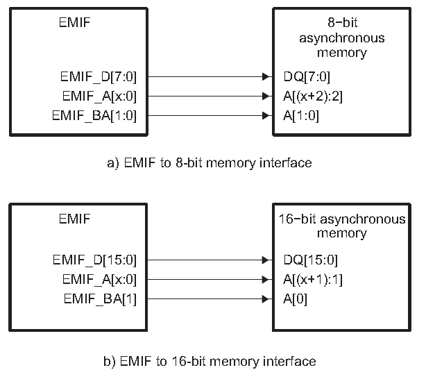
The EMIF address pin EMIF_A[0] always provides the least-significant bit of a 32-bit word address. Therefore, when interfacing to a 16-bit or 8-bit asynchronous device, the EMIF_BA[1] and EMIF_BA[0] pins provide the least-significant bits of the halfword or byte address, respectively. Additionally, when the EMIF interfaces to a 16-bit asynchronous device, the EMIF_BA[0] pin can serve as the upper address line (EMIF_ADDR[22] for RM57/TMS570LC43x, or EMIF_ADDR[13] for RM46/TMS570LS12x). Weak pullups are recommended on chip selects
Figure 8-1 shows the mapping between the EMIF and the connected device’s data and address pins for various programmed data bus widths. The data bus width may be configured in the asynchronous n configuration register (CEnCFG).
5.1.9. Universal Serial Bus (USB)
Three USB ports are provided on several Hercules devices (RM48, RM46), and two of them may be used simultaneously. Hercules device provides USB controller only, so an external USB transceiver is needed for each USB port.
The USB module on those devices supports the following configurations: 1 USB Host Port + 1 USB Device Port, OR 2 USB Host Ports Interface signals for the USB host port #2 are multiplexed with interface signals for the USB device port. If the application requires the use of the USB device port, then the USB host port #2 must first be powered down. For pin multiplex, and signals mapping between MCU and the transceiver, please refer to the Technical Reference Manual (TRM).
It is important to provide transient suppression for USB connectors. For best ESD and EMI performance, create a chassis ground to which the metal shield of the USB connector is connected.
5.1.10. Serial Communication Ports (SPI, SCI, LIN, I2C, and CAN)
Normally SPI and I2C are board-level interfaces that are connected to other devices on the board. Pay close attention to the drive capability and trace length, which depends on the selected frequency of these signals. SCL and SDA pins of the I2C must be externally pulled-up to 3.3V for proper operation.
SCI, LIN and CAN interfaces require transceivers to transform the signal into the required electrical signaling. CAN bus network must have a terminating resistor between CAN_H and CAN_L for it to work properly. The typical termination is one 120 ohm resistor at each end of the bus.
5.1.11. Quadrature Encoder Pulse (eQEP)
Some Hercules devices support connection to a quadrature encoder that tracks position, direction of rotation, and estimates velocity. The frequency of the eQEP inputs can be as high as ¼ of the CPU frequency. Pins used for the eQEP are eQEPxA, eQExB, eQEPxI and eQEPxS.
A series resistor followed by a capacitor to digital ground should be placed on each eQEP input to filter the inputs from noise that would violate the input electrical specifications of the device. A common value for the series resistor is 100Ω and for the capacitor is 1nF.
5.1.12. Series Termination Resistors
As a general rule, transmission line (trace) termination is necessary when the round trip propagation time of the signal is equal to or greater than the transition (rise or fall) time of the driver; otherwise, there will be data errors caused by signal degradation, line noise, and, reflections. Series termination is effective in reducing the driver’s edge rate, and it consumes low power. It is recommended for single receiver, point-to-point and star topologies. Series termination provides good signal quality by damping overshoot and undershoot, and effectively reducing line noise and EMI. Its drawbacks are that it slows the signal’s rise and fall time, and that it should not be used with distributed loads.
Output series termination is best placed within 0.5 in (12.7 mm) of the output pin. The values used are system dependent but often are one of 10 ohms, 22 ohms or 33 ohms.
For distributed loads, AC termination is recommended. the RC time constant should be greater than the transmission line’s round-trip propagation time.
5.1.13. Power Supply
The Hercules devices have multiple power supply pins. This includes: • CPU core supply (VCC) • Digital I/O logic supply voltage (VCCIO) • ADC analog supply voltage (VCCAD) • ADC reference source (ADREFHI, ADCREFLO) • Flash pump supply voltage (VCCP) • Digital logic supply ground (VSS) • ADC analog ground (VSSAD)
All the power supply pins must be connected for proper operation. All Hercules devices have multiple supply pins for the core, I/O, and ADC supplies. All such pins must be connected to the proper supply voltage for proper operation. Do not leave any of the supply pins unconnected. The voltage level for I/O pins and flash pump is 3.3 V; whereas, the core supply voltage is either 1.2. For more information, see the Electrical Specifications section of the device-specific data sheets.
5.1.13.1. Power Sequencing
A voltage monitor (VMON) is implemented on all the Hercules devices. The use of VMON eliminates the requirement for a specific sequence when powering up the core and I/O voltage supplies.
It is recommended that no voltage larger than a diode drop (0.7 V) should be applied to any input pin prior to powering up the device. Voltages applied to pins of an unpowered device can bias internal p-n junctions in unintended ways and produce unpredictable results.
The Hercules devices need to follow the power-down sequencing. During power-down, the nPORRST should be asserted low at least 1ms before the VCCIO supply reaches 1.14 V. This helps to keep on-chip flash logic in reset prior to the VCCIO/VCC power supplies ramping down.
It is recommended that you use the external voltage supervisors to meet this constraint.
5.1.13.2. Decoupling Capacitors
Hercules devices are fabricated using advanced CMOS technology. The CMOS circuits draw large currents at every transition, producing current spikes on the supply rails. These rising and falling glitches have to be filtered before they traverse into the sensitive circuit area. The bypass or decoupling capacitors placed across power supply pins and ground are used for such filtering.
Hercules devices have several power supply pins. You need to use one capacitor on each power supply pin and should place this capacitor as close to the pin as possible, without using any via. Typically small (100nF), low-ESR ceramic capacitors are used for this purpose.
Adding bypass capacitors to the analog supply pins helps reduce power-supply noise entering the analog circuit.
5.1.13.3. ESD Protection
Hercules devices comply with TI standard ESD specifications and are tested for ESD compliance. Hercules devices offer device-level ESD specifications like the charge device model (CDM, ±500 V for all pins and ±750V for corner pins) and the human body model (HBM, ±2.0 KV). Device level ESD specifications are not sufficient to protect devices in a system. The energy associated with a system-level ESD strike is much higher than a device-level ESD strike.
Any signal from the Hercules microcontroller that is exposed outside the system enclosure via a connector should have an ESD protection.
5.2. PCB Layout Guidlines
..Note:: under construction