8.1. FreeRTOS FAQ
What are Data Abort and Prefetch Abort and how do I debug them?
When Cortex-R4/R4F/R5F can’t access memory successfully, an abort is generated. An error occurring on an instruction fetch generates a prefectch abort (PABT), and errors occurring on data accesses generate data abort (DABT).
Some of the reasons for the abort are: - a permission fault indicated by the MPU - an error response to a transaction on the AXI/AMBA memory bus - an error detected in the data by the ECC checking logic
Hence, a Prefetch Abort is an indication of an attempted illegal memory access which can be caused by attempting to access invalid instruction memory. It can be caused, for example, by double-bit ECC error, or MPU configuration not having correct permission, etc.
A Data Abort is an indication from a memory system to a core when there is an atempt to access invalid data memory. It could be caused by memory location not being implemented, memory location being read or write only in Privileged Mode (when processor is in User Mode), error being detected in the data by ECC checking logic, or etc.
When an abort happens, the fault status and fault address can be retrieved through CP15 registers. The CP15 IFAR, Instruction Fault Address Register, holds the address of instructions that cause a prefetch abort. The CP15 DFAR, Data Fault Address Register, holds the address of the fault when a precise abort occurs.
The Fault Status Registers, IFSR and DFSR, record the type of abort that occruurd, and whether on a read or a write. These registers will help to identify the offending code.
How can I have more than one timer?
HalCoGen FreeRTOS template doesn’t allow to setup 1-3 RTI compare modules. The second RTI compare will need to be enabled manually. The RTI configuration is in the function of prvSetupTimerInterrupt(void) in os_port.c. The complete procedure of manually adding a additional timer (for example a 5 ms timer) in addition to a 1ms timer gernated by HalCoGen FreeRTOS is:
In HalCoGen “VIM RAM” rename to “rtiCompare1Interrupt” interrupt 0x00000010:03
In HalCoGen “VIM CHANNEL 0-31” enable interrupt 3 RTI Compare 1
In HalCoGen generate code
added HL_RTI.h
added HL_reg_RTI.h
added HL_RTI.c
in os_port.c add the following lines at the end of method prvSetupTimerInterrupt
/* Enable 5ms compare1 timer */
portRTI_CNT0_COMP1_REG = portRTI_CNT0_COMP0_REG * 5; //5ms
portRTI_CNT0_UDCP1_REG = portRTI_CNT0_UDCP0_REG * 5; //5ms
portRTI_SETINTENA_REG = 0x03;
add the following lines inside /* USER CODE BEGIN (2) */
#define portRTI_CNT0_COMP1_REG ( * ( ( volatile uint32_t * ) 0xFFFFFC58 ) )
#define portRTI_CNT0_UDCP1_REG ( * ( ( volatile uint32_t * ) 0xFFFFFC5C ) )
where is needed in your code, add:
#include "HL_reg_rti.h"
#include "HL_rti.h"

void rtiNotification(rtiBASE_t *rtiREG, uint32 notification)
{
    gioSetBit(hetPORT1, 0, gioGetBit(hetPORT1, 0) ^ 1);
}
Why aren’t IP packets sent when using LWIP with FreeRTOS?
When running LWIP with FreeRTOS using static IP address, everything seems fine with link status up, but the pnig fails, or no data sending out of the Hercules Ethernet port.
These may be related to the MPU configuration if the devices support Cache. The configuration for MPU regions need to be type of NORMAL_OIWTNOWA_NONSHARED (Cache Write-Through). If using HalCoGen FreeRTOS, the MPU settings for the first 4 regions are grayed out and not configurable. They will need to set manually in vPortStoreTaskMPUSettings() in os_port.c
How to debug FreeRTOS stack overflow issue?
Usually, when a stack overflow occurs, it can cause a Data Entry Interrupt. From the LR register, the offending address and function can be located. Depending on which function causes the issue, one of the stack size may need to be adjusted.
TI has scripts from cg_xml package in Code Generation Tools XML Processing Utilities which can be used to perform static stack analysis. Please refer to the CodeGen Tool page for detailed info which might be helpful:
8.2. F021 Flash FAQ
Hercules F021 Flash API is a library of routines that when called with the proper parameters in the proper sequence, erases, programs, or verifies flash memory on Hercules microcontrollers using the F021(65nm) process. These routines must be run in a privileged mode to allow access to the flash memory controller registers.
- Can F021 Flash APIs run in user mode?
No, the F021 Flash APIs must be run in a privileged mode (a mode other than user) to allow access to the Flash memory controller registers.
- How does RWAIT work?
The CPU runs faster than the flash memory. Wait states are cycles the CPU must wait in order to retrieve data from the flash memory which has access times longer than a CPU clock.
The TCM flash (flash on Cortex-R4 devices) can support zero address and data wait states up to a CPU speed of 55 MHz in non-pipelined mode. The TCM flash supports a maximum CPU clock speed of 220 MHz in pipelined mode with one address wait state and three data wait states.
L2FMC (Flash on Cortex-R5F devices) can support zero data wait state up to 45 MHz in non-pipelined mode. L2 flash is clocked by HCLK and is limited to maximum 150 MHz.
The number of wait states is correlated to HCLK frequency. The required wait states for each HCLK frequency can be found in the device-specific data sheet.
- Can we change the device system clock before erasing or programming the flash?
Yes, but the Fapi_initializeFlashBanks(), and Fapi_setActiveFlashBank() must be called again before any asynchronous flash operations.
- How to calculate and program ECC to ECC space when programming the data to flash?
There are four programming modes of Fapi_issueProgrammingCommand(). Fapi_AutoEccGeneration will enable the API to be used to program the supplied data portion in Flash along with automatically generated ECC. ECC is calculated on 64-bit aligned addresses up to the data width of the bank.
- Can I use big data buffer when programming the flash using Fapi_issueProgrammingCommand()?
The size of the data buffer can be any size between 1 bytes and the flash bank width. The bank width of TCM flash (flash on Cortex-R4 devices) is 16 bytes, and the bank width of L2FMC is 32 bytes. Please find the bank width in flash bank configuration register (FCFG_BANK ).
- Can we erase/program one flash sector in the same bank?
All of the Flash APIs that program, erase, blank check or margin verify must be called from a bank other than the one in which code is being executed. If programming or erasing bank 0 of the device which has only one flash bank, these routines must be executed in RAM.
- Does Cortex-R5F device use the same flash API library as Cortex-R4F device?
No, they use different flash API library. Cortex-R5F devices (TMS570LC43x, and RM57Lx) use L2FMC flash memory controller which is different from TCM flash used on Cortex-R4 devices. The flash API library with the suffix of “_L2FMC”
- Why do I get error when performing blank check on TMC570LC43x device?
The flash memory is protected by Single Error Correction Double Error Detection (SECDED). On this Cortex-R5 based device, ECC is enabled by default. Erasing is done on Flash memory without the ECC being programmed. So reading a location with invalid ECC will generate correctable or uncorrectable error.
- Are Interrupts disabled inside the Flash APIs?
The interrupts are not disabled inside the flash APIs. It is recommended that you disable the interrupts before calling flash API.
- Can Flash API library run from RAM instead of Flash?
Yes, it is possible. Please refer to CAN bootloader examples in Hercules examples git repo. http://git.ti.com/hercules_examples
- Is it mandatory to use the F021 Flash API to erase/program the Flash on Hercules parts?
Use of F021 Flash API is mandatory for anyone implementing routines to erase / program Flash memory on Hercules parts.
- Can I get the source code for the F021 Flash API?
Yes, the source code can be provided with a NDA. However, recompiling or redistributing the source is not allowed.
- What is the compiler version used for generating the F021 Flash API library?
F021 Flash API was compiled using TI’s code generation tools for ARM version 5.1.3.
- Can the F021 Flash API be compiled with newer version of the ARM Compiler from TI / IAR / KEIL / GCC?
The F021 Flash API library is distributed in the ARM standard EABI ELF format and is compiled using TI’s code generation tools for ARM version 5.1.3. Users are not expected to recompile this library in any way, as then the specified functionality is not verified / supported any more.
- Can this F021 Flash library be used in code projects using any other tool chain? Are there any constraints or restrictions?
The F021 Flash API library can be used in any code project that uses tools compliant to the ARM standard EABI format.
- Is therte an example of using F021 Flas APIs?
Yes. Examples using F021 Flash API can typically be found in bootloader code. Please refer to CAN bootloader as example:
Please refer to readme.txt to import the CAN bootloader for a particular platform into Code Composer Studio.
The F021 Flash API is called from .\SafetyMCU_Bootloaders\source\bl_flash.c.
bl_flash.c can be used as a reference to implement your application specific functions to call F021 Flash APIs.
- Is the F021 Flash API compatible to IAR?
The F021 library is compatible with IAR v7.x and older version compiler, abd incompatible with IAR C 8.x compiler:
The F021 Flash API library is okay to use in IAR projects that require using the flash API up to v7.x of IAR’s ARM compiler. Starting from v8.x of IAR ARM compiler, the wchar data type was changed to be 32-bit wide instead of 16-bit wide. This causes warnings to be created any time someone uses any library not compiled using IAR’s v8.x. Safety-critical application developers are not allowed to ignore compiler warnings.
The solution is to use the old IAR C 7.x compiler.
8.3. Emulated EEPROM (FEE)
Many applications require storing small quantities of system related data (e.g., calibration values, device configuration) in a non-volatile memory, so that it can be used or modified and reused even after power cycling the system. EEPROMs are primarily used for this purpose. EEPROMs have the ability to erase and write individual bytes of memory many times over and the programmed locations retain the data over a long period even when the system is powered down.
The Hercules devices do not have a traditional EEPROM on the chip. The objective of TI FEE Driver is to provide a set of software functions intended to use a sector of on-chip Flash memory as the emulated EEPROM (FEE). These software functions are transparently used by the application program for writing, reading and modifying the data.
The Hercules devices do not have a traditional EEPROM on the chip. The objective of TI FEE Driver is to provide a set of software functions intended to use a sector of on-chip Flash memory as the emulated EEPROM (FEE). These software functions are transparently used by the application program for writing, reading and modifying the data.
What are the difference between EEPROM and Flash Emulated EEPROM (FEE)?
The EEPROM is connected to the host microcontroller via a serial interface. The I2C and SPI are quite popular due to the minimal number of pins. The most of EEPROM allows byte-by-byte program or erase operations. Compared to EEPROM, FEE has higher density. Every FEE location reads 0xFFFF after erased. Through programming, the cell can be changed to logical 0. Any word can be overwritten to change a bit from logical 1 to 0; but not the other way.
The major difference between EEPROM and FEE is the time for write and erase. A typical FEE write time is 40µs/144-bit word; whereas, EEPROM typically requires 5 to 10ms.
Is emulated EEPROM protected by ECC?
Yes, access to the FEE flash bank (bank 7) is protected by dedicated SECDED logic inside the digital interface to the flash banks. The ECC protection on Cortex-R5F based Hercules devices (TMS570LC43x, and RM57Lx) is enabled by default. The ECC protection on Cortex-R4/R4F based Hercules devices (TMS570LSx, and RM4xLx) is disabled by default.
How to enable FEE ECC check?
On Cortex-R4 based Hercules devices, the ECC protection for accesses to the EEPROM emulation flash bank can be enabled by writing 0xA to the EE_EDACEN field of the flash module’s Error Correction Control Register 1 (EE_CTRL1).
How can I enable the single and double bit Error Corrections?
FEE software provides a mechanism to detect single and double bit errors. In order to use this feature, application has to make sure that “EE_EDACMODE[3:0]: Error Correction Mode” in “EE_CTRL1” should be set to a value other than 0101, “EE_ONE_EN: Error on One Fail Enable” should be enabled, “EE_ZERO_EN: Error on Zero Fail Enable” should be enabled, “EE_EDACEN[3:0]: Error Detection and Correction Enable” should be set to a value other than 0101.
Is Checksum used for FEE block protection?
Yes, CRC checksum is an option in FEE block header. If CRC is enabled, during writing of a block, CRC of the data to be written is calculated and checked against the CRC of the same block which is already existing in FEE Flash. If CRC matches, data is not written. If CRC is not enabled, then data is compared byte by byte. If data does not match, write will be initiated.
What is the Checksum algorithm used in FEE driver?
The algorithm used in FEE driver is Fletcher-16 checksum.
What is the weakness of Fletcher-16 checksum?
The Fletcher-16 checksum cannot distinguish between blocks of all 0 bits and blocks of all 1 bits. For example, if a 16-bit block in the data word changes from 0x0000 to 0xFFFF, the Fletcher checksum remains the same. This also means a sequence of all 00 bytes has the same checksum as a sequence (of the same size) of all FF bytes.
Can we call all the FEE APIs in USER mode?
No. FEE needs following API’s to be executed in Privilege mode: TI_Fee_Init, and TI_FeeInternal_WriteDataF021
Can I call TI_Fee_Init() API more than one time?
No. TI_Fee_Init() provides functionality for initializing the TI FEE module. This routine must be called only once at the beginning before commencing any data operation.
- Can I call TI_Fee_Init() API more than one time?
No. TI_Fee_Init() provides functionality for initializing the TI FEE module. This routine must be called only once at the beginning before commencing any data operation.
- What happens if there is a RESET during flash is been erasing?
In next initialization, this sector is added to the erase queue since sector header will not match with the expected sector header states (Active, Copy, Ready for Erase, Empty). Erasing will happen in the background.
- What happens if there is a RESET during writing data?
Block is written in following way:
- Block status is programmed as start program block.
- Block number and block size are written.
- Write data of the block.
- After completion of writing of data, Checksum and address of previous block are written
- Block status is marked as Active.
If reset happens after setp 1, then in next initialization, writing of next block is shifted by 24 bytes. If reset happens after step 2, step 3, step 4 or step 5, then the writing of next block will happen after current block size + block header.
- Can I call TI_Fee_Init() API more than one time?
No. TI_Fee_Init() provides functionality for initializing the TI FEE module. This routine must be called only once at the beginning before commencing any data operation.
- Can I run FEE operation in interrupt ISR?
We strongly recommend not to use Flash Sync Operation (FEE Write especially) inside ISR. FEE write can initiate an Flash Erase operation during the Page Swap (i.e., if Virtual Sector is full and moves to different Virtual Sector and perform erase of old Virtual sector). which could take considerable amount of time and also it varied from device to device and with ageing too.
You can initiate a Async Write (TI_Fee_WriteAsync) inside ISR and perform TI_Fee_Mainfunction outside of ISR. The actual write is performed in TI_Fee_MainFunction.
8.4. DCAN Remote Frame FAQ
What is the remote frame used for?
The intended purpose of the remote frame is to solicit the transmission of data from another node.
What is the difference between remote frame and data frame?
There are four different CAN message frames or types that can be transmitted on CAN bus: Data frame, remote frame, Error frame, and Overload frame.
The Data frame is the most common message type, and the data frame is used by the transmitter to send a message to the receiver. The remote frame is similar to the data frame, with two important differences. First, this type of message is explicitly marked as a remote frame by a recessive RTR bit in the arbitration field, and secondly, tere is no data. The remote frame is used by a receiver to to request transmission of a message that has the same ID from the transmitter.
Is a transmit object used for remote frame?
No, the remote frame is stored in a receive object. Setting the TxRqst bit of a receive object will cause the transmission of a Remote Frame with the receive object’s identifier. This Remote Frame triggers the other CAN node to start the transmission of the matching Data Frame.
Should the DLC of remote frame be identical to the DLC of the corresponding (requested) data frame?
No, the DLC of remote frame doesn’t affect the data length code (DLC) of the requested data frame. The requested CAN node needs to knw the correct DLC.
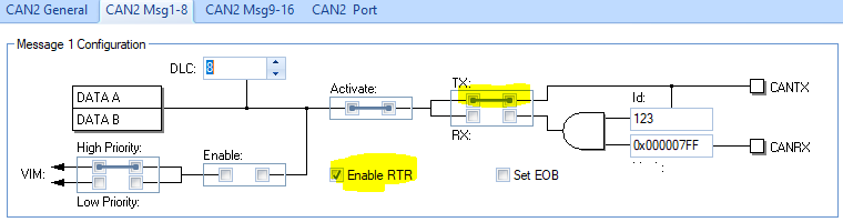
How to configure the remote frame?
The message object for the remore frame should be configured as “receive” (DIR=0). Please refer to the example code in example folder.
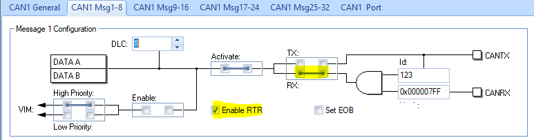
How to configure the requested data frame to response the remote frame automatically?
To receive a remote frame, the message object should be configiued as transmitter with RmtEN enabled. The data field should be filled before enabling the RmtEN (remote).
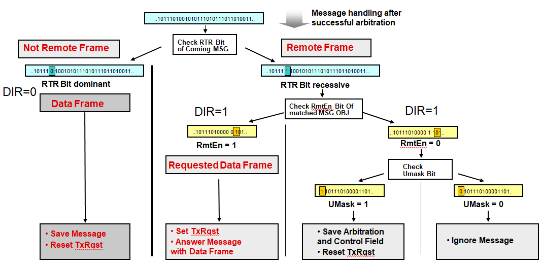
When a Remote Frame is received, three different configurations of the matching message object have to be considered:
1. Dir = 1 (direction = transmit), RmtEn = 1, UMask = 1 or 0. The TxRqst bit of this message object is set at the reception of a matching Remote Frame. The rest of the message object remains unchanged. 2. Dir = 1 (direction = transmit), RmtEn = 0, UMask = 0. The Remote Frame is ignored, this message object remains unchanged. 3. Dir = 1 (direction = transmit), RmtEn = 0, UMask = 1. The Remote Frame is treated similar to a received Data Frame. At the reception of a matching Remote Frame, the TxRqst bit of this message object is reset. The arbitration and control bits (Identifier + IDE + RTR + DLC) from the shift register are stored in the message object in the Message RAM and the NewDat bit of this message object is set. The data bytes of the message object remain unchanged.
Please refer to the example code in example folder.
8.5. JTAG Connection
Is JTAG RTCK required for target connection?
RTCK is not a standard JTAG signal. The asynchronous TAP controller does not require local synchronization, so the RTCK is not a MSUT.
But, occasionally a target device requires the JTAG interface to be externally synchronized to a clock within the device due to it being slow, non-continuous, or variable. The adaptive clocking feature uses the RTCK to address this requirement. When adaptive clocking is enabled, the debug unit issues a TCK signal and waits for the RTCK signal to return before sampling TDO.
If you emulator supports adaptive clock feature, and you are planning to use this feature, you need RTCK from the target device.
What are the dfifference between JTAG and ETM?
JTAG: The functionality usually offered by JTAG is Debug Access and Boundary Scan: 1. Debug Access is used by debugger tools (for example XDS110, XDS2x) to access the internals of a chip making its resources and functionality available and modifiable, e.g. registers, memories and the system state. 2. Boundary Scan is used by hardware test tools to test the physical connection of a device, e.g. on a PCB. This is usually not the task of a debugger tool.
ETM: The Embedded Trace Macrocell (ETM) interface enables you to connect an external ETM unit (for example XDS560V2 Pro) to the processor for real-time code tracing of the core. JTAG signals are also required for ETM trace.
Why should the nTRST signal be pulled LOW?
nTRST is JTAG “Test Reset”. It is low active. The nTRST is used for an asynchronous reset of the state machine of the JTAG Test Access Port (TAP). The debugger drives it by a push-pull driver. It resets the TAP by a certain JTAG sequence. The target device requires that the nTRST is first held low for a few TCK cycles and then raised after the TCK signal has started running, so the device can detect a rising edge on nTRST.
A pull-down resistor should be added onto nTRST on target side. It ensures the on-chip debug logic is inactive when the debugger is not connected.
From the debugger point of view, nTRST is optional.
The JTAG connection is lost after the program is loaded to flash.
The problem might be caused by the code you have programmed. The code in the flash makes the CPU enter an exception state repeatedly, and the CPU is not able to enter a debug state.
Please try this procedure to let CPU enter a debug state:
- Open the target configuration window, and launch the selected the configuration
- Switch to debug window.
- Press the reset (nRST) button and hold it.
- Click “Connect Target” immediately after you release the nRST button.
- The board should be connected after couple tries.
Unable to access the target device through JTAG
Try the following steps:
- From the View menu in CCS open the Target Configuration View.
- Find the .ccxml file that is part of your project.
- Right click on it and choose “Launch selected configuration”. This will start a debug session in CCS but won’t connect to anything yet.
- When the debug view opens click on the top level node in the tree (it will be the name of the .ccxml file). Select “Show all cores”.
- Under “Non debuggable devices” select the one that ends in ICEPick_C.
- Click on the connect button on the toolbar.
- Open the registers view.
- If you expand core registers. Do the TAP registers have values other than 0 or 1?
- Next select the DAP under “Non debuggable devices” and see if you can connect to that.
8.6. High End Timer (N2HET)
The N2HET is an advanced intelligent timer that provides sophisticated timing functions for real-time applications. The timer is software-controlled, with a specialized timer micromachine and an attached I/O port. The N2HET can be used for pulse-width-modulated outputs, capture or compare inputs, or GPIO. The High-End Timer Transfer Unit (HTU) can perform DMA-type transactions to transfer N2HET data to or from main memory.
Can we use N2HET pins for another purpose?
Each NHET channel can be independently controlled either by the timer program or via the general-purpose I/O control registers. If you have an NHET2 pin that needs to be configured as a general-purpose output, please ensure that the NHET2 timer program does not use this pin as an output function.
Should the N2HET RAM be initialized before using?
After device power up, the N2HET RAM contents including the parity bits cannot be guaranteed. In order to avoid false parity failures due to the random state in which RAM powers up, the RAM has to be initialized.
Before initializing the N2HET RAM, the N2HET parity logic needs to be enabled. With parity enabled, the N2HET parity RAM will be initialized automatically by N2HET at the same time that the N2HET instruction RAM is initialized by the CPU
How to initialize the N2HET RAM?
To start with a clean N2HET RAM ,the complete N2HET RAM has to be initialized with zeros and the parity bits set accordingly by configuring the following registers in the system module: • Memory Hardware Initialization Global Control Register (MINITGCR) • Memory Initialization Enable Register (MSINENA) For more details on RAM hardware initialization support, refer to the system module reference guide.
How to select the Loop resolution time (LRP)?
The timer program is a set of instructions executed sequentially, one after the other. Reaching the end, the timer program restarts on every resolution loop. The start address is fixed at N2HET RAM address 00h.
Most instructions execute in one cycle (VCLK2 cycles), but a few take two or three cycles (VCLK2 cycles).
The loop resolution period (LRP) must be selected to be larger than the number of time slots (VCLK2 cycles) required to complete the worst-case execution path through the N2HET program. Otherwise a program overflow condition may occur.
What are the architectural restrictions on N2HET programs?
Four restrictions apply to N2HET programs: • The size of an N2HET program must be greater than one instruction. • An extra wait state is incurred by any instruction that modifies a field in the next instruction to be executed. • Only one instruction (using high resolution) is allowed per high resolution pin. • Consecutive break points are not supported. Instructions with break points must have at least a distance of two instructions. To enforce restriction #3, the high resolution pin structures respond only to the first instruction that is executed matching their pin number with hr_lr=HIGH, regardless of whether or not the en_pin_action field is ON. Subsequent instructions are ignored by the high resolution pin structure for the remainder of the loop resolution period.
How to check the parity detection logic of N2HET RAM?
The N2HET RAM is organized into two sections. The first contains the N2HET program itself. The second contains parity protection bits for the N2HET program.
To test the parity detection logic, the N2HET parity RAM has to be made accessible to the CPU in order to allow a diagnostic program to insert parity errors. The control register bit HETPCR.TEST must be set in order to make the parity RAM accessible.
What is the HR structure Sharing used for?
The HR Structure Sharing allows two HR structures to share the same pin for input capture only. If the bits in HETHRSH are set, the HR structures N and N+1 are connected to pin N. In this structure, pin N+1 remains available for general-purpose input/output.
How does XOR-shared HR Structure work?
Usually the N2HET design allows only one HR structure to generate HR edges on a pin configured as output pin. The HETXOR register allow a logical XOR of the output signals of two consecutive HR structures N (even) and N+1 (odd).
In this way, it is possible to generate pulses smaller than the loop resolution clock since both edges can be generated by two independent HR structures. This is especially required for symmetrical PWM.
8.7. CPU Compare Module Selftest FAQ
- Do I have to initialize the MCU registers during system start-up?
Yes. Not all internal registers of the Cortex-R4F CPU have fixed values upon reset. To avoid an erroneous CCMR4F compare error, the application software needs to ensure that the CPU registers of both CPUs are initialized with the same values before the registers are used, including function calls where the register values are pushed onto the stack.
- Do I have to dissable the IRQ and FIQ before running CCM-R4F selftest?
Yes, the CCM selftest is not interruptable.
- Why does CCM-R4F self-test get stuck?
CCM selftest needs to be run when the debugger is not connected. Certain debug operations place the CPU in a halting debug state where the code execution is halted. Because halting debug events are asynchronous, there is a possibility for the debug requests to cause loss of lockstep. CCM-R4F will disable upon detection of halting debug requests. Core compare error will not be generated and flags will not update. A CPU reset is needed to ensure the CPUs are again in lockstep and will also re-enable the CCM-R4F.
The Error flags generated by CCM-R4F in 4 operating modes?
CCM-R4F Mode Key CCM-R4 Selftest Failure
ESM 1.31
CCM-R4 Compare Failure
ESM 2.2
Lock-step Mode 0000b Enabled Enabled Self-test Mode 0110b Enabled Disabled Error Forcing Mode 1001b Error Error Self-test Error Forcing Mode 1111b Error Enabled
The CCM-R4F module has four operating modes, each with its own purpose:
- Self-test error forcing mode: this mode ensures that any error during the self-test of the CCM-R4 compare logic itself is actually flagged as a self-test error in the CCM-R4 status register. This also sets the CCM-R4 self-test error flag in the ESM (group 1 channel 31). The application must look for these error flags to become set and then clear them. The compare error flag is not set in this mode.
- Self-test mode: this mode runs the actual self-test on the CCM-R4 logic. This self-test is expected to pass. Any error is indicated on the STE flag inside CCM-R4 as well as on ESM group1 channel 31. This is a real error which indicates that the CCM-R4 logic cannot be verified to be correct.
- Error-forcing mode: this mode actually forces a compare error from the CCM-R4 module. This causes the compare error as well as the self-test error flags to be set inside the CCM module. Also the corresponding ESM flags are set. This mode checks that the CCM-R4 compare error output is not stuck-low, and that the connection between the CCM-R4 module and the ESM group2 channel 2 is okay. Once the application detects that the appropriate flags are indeed set, these flags can be cleared and the CCM-R4F module can be restored to be in lock-step compare mode.
- Lock-step mode: this is the default mode.
- Can nERROR pin directly connect to nRST pin?
It is not recommended to directly connect the nERROR signal to the nRST signal. The nERROR signal can be driven out by the application when running a self-check on the nERROR pin itself, or when running a self-test on the CPU Compare Module. Instead, the nERROR signal needs to be monitored by a smart logic which can respond to the nERROR signal being driven low once the application has indicated that it is now done with all the self-tests that use the nERROR signal.
- How do I know if the nERROR pin functions properly?
The error response generation mechanism is testable by software by forcing an error condition. This allows testing the nERROR pin functionality. By writing a dedicated key to the ESM Error Key Register (ESMEKR), the nERROR pin is set to low for the specified time.
- Why are there 2 ESM status registers for group 2?
There are two status registers or ESM group 2: ESMSR2 (status register 2) and ESMSSR2 (status shadow register 2). If an error occurs in Group 2, the ESM module will set the corresponding error flags in ESMSR2 and ESMSSR2. If an RST is triggered or the error interrupt has been served, the error flag of Group2 should be read from ESMSSR2 because the error flag in ESMSR2 will be cleared by RST.
- nERROR pin is connected to another device. When the nERROR is asserted, how does the device know the error source?
There is no way for the external monitor circuit outside microcontroller to identify the source of the error.
- Is there any way to disable CCM-R4F Lock-step?
The CCM-R4F will compare all the time unless you put the CCM-R4F in test mode and leave it in test mode. In this test mode, it will not check and report any error.
- I am using Hercules Cortex-R5F HDK (TMS570LC43x HDK, and RM57Lx HDK). As soon as the debugger is connected to the target (TMS570LC43x, or RM57Lx), the nERROR LED is turned on. ESM status indicates a CPU compare error.
In CCM-R4 or CCM-R5 the logic is that the compare will be disabled when the CPU is in debug state. The reason is that a debug event is asynchronous. It is possible the asynchronous debug requests can cause the CPUs to be out of lockstep (documented in TRM). The CCM will remain in disable state until a power up reset is generated. This is why we ask users not to do CCM self test when in debug mode.
The difference between LSxx devices and LC43xx devices is on the debug state broadcasting. In LSxx devices, the signal that indicates the CPU is in debug mode is broadcasted to the rest of the sytem. Everyone sees it including the CCMR4. As soon as CCM-R4 sees the DBGACKm signal it stops to compare. In LC43xx the DBGACKm is first routed to the on-chip CTI (Cross Trigger Interface). By default, the CTI is disabled. Therefore, the CTI actually disable the DBGACKm from broadcasting to the rest of the system. So CCM-R5F never sees the CPU in the debug state and continues to compare even in debug mode. But once you enable CTI (CCS->Scripts), you will see proper behavior. However, for the problem that you are seeing, it is right at the connection time and you have not the CTI enabled yet.
8.8. Flash Diagnostic Modes FAQ
The Flash wrapper can be put in diagnostic mode to verify various logic. There are multiple diagnostic modes supported by the wrapper. A specific diagnostic mode is selected via the DIAG_MODE control bits in the diagnostic control register (FDIAGCTRL),
What is the usage of the Flash Mirror?
The mirrored flash is mainly used for diagnostic. Normally the flash memory is mapped to starting address at 0x0 of the CPU’s memory map. However, the flash memory is also mapped to 0x20000000 in the CPU’s memory map.
The mirrored flash has he same content as the main flash does. Any data written to the main flash will be reflected in the mirrored flash. They are physically the same memory. The flash can not be erased and programmed using the address of mirrored flash (staring from 0x20000000)
Can I run diagnostic mode 1 for main program flash?
No. The diagnostic mode 1 is for ECC diagnostic on the bus2 (used to access EEPROM). The flash wrapper has two buses, the bus1 and bus2. The bus1 is used by the CPU to access the program flash for which the program and data are stored. The CPU will use the bus2 to access the OTP sectors, EEPROM emulation flash bank. When CPU accesses the program flash via bus1, the CPU’s built-in SECDED logic will perform the ECC checking. Note this ECC logic is inside the CPU, not inside the flash wrapper. When CPU accesses via bus2 for the EEPROM bank or the OTP sectors the ECC checking is done inside the flash wrapper. The reason is that the CPU’s level 2 interface (AXI-M bus) which is connected to the flash memory system’s bus2 does not have ECC checking capability. Therefore, the flash wrapper has its own ECC logic just for bus2 accesses.
Flash diagnostic test uses data from the ECC syndrome. How is the value in syndrome table calculated?
According the ECC encoding table in TRM, for one ECC bit (ECC[x]), we need to XOR all address and data bits marked with an “x” in the table (Table 5-1, in TMS570LS31x TRM), and additionally if “parity” is marked as “odd” the row needs to be XOR’ed with “1”. If parity is “EVEN” then the result of the row is already the ECC[x] bit.
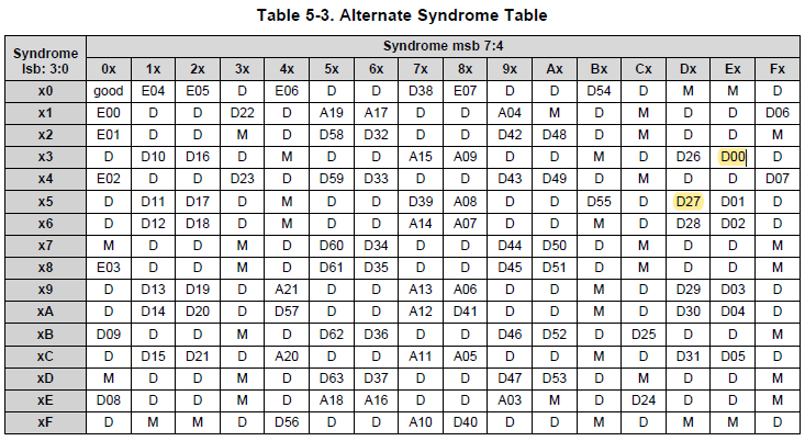
Example 1: For address 0x00000000 and data 0x00000000, the ECC is 0x0C. The ECC result for address 0x00000000 and data 0x00000001 is 0xEF. The syndrome is 0x0C XOR 0xEF = 0xE3 for single data bit 0 error at address 0x00000000.
Example 2: For address 0x00000000 and data 0x00000000, the ECC is 0x0C. The ECC result for address 0x00000000 and data 0x08000000 is 0xD9. The syndrome is 0x0C XOR 0xD9 = 0xD5 for single data bit 27 error at address 0x00000000.
Difference of ECC detection and correction between program flash and FEE?
The CPU is checking the ECC for memories on the ATCM and BTCM and the Flash Wrapper is checking the ECC for the EEPROM region.
Why should a developer use the SafeTI Diagnostics Library?
SafeTI Diagnostics Library followed the ASILD/SIL3 software development process. TI provides the SafeTI Diagnostics Library in the form of a library and also source files for maximum flexibility to customers. It can be used along with or independent of HALCoGen.
Can I use HALCoGen with the SafeTI Diagnostic Library?
Yes, HALCoGen has a safety library example. This example describes the steps to create a sample startup which configures and runs safety diagnostic tests using the SafeTI Diagnostic Library. Open HALCoGen –> Help –> Help Topics –> Contents (left panel) –> Examples –> example_SafetyLib.c. Click example_SafetyLib.c, the right panel will show the steps.
Which of these routines does TI recommend customers use?
HALCoGen Safety Function was developed long before SafeTI Diagnostics Library was available. So for legacy reasons HALCoGen still supports these safety functions with respect to boot code. There is still a need to evaluate run time and periodic needs for diagnostic execution according to the application specific FTTI requirements. Each customer is encouraged to evaluate the specific needs of their project in regard to their safety requirements and development schedules and although it is not a requirement for system certification, the use of the SafeTI Diagnostics Library can aid in time to market since many of the safety mechanisms described in the device specific safety manuals are implemented in the SafeTI Diagnostics Library. This allows for a faster understanding of the diagnostic measures as well as faster implementation in the application level code.
** Continue ...**
8.9. Troubleshooting Abort Exceptions
What are exceptions?
An “Exception” is an event that makes the processor temporarily halt the normal flow of program execution, for example, to service an interrupt from a peripheral. Before attempting to handle an exception, the processor preserves the critical parts of the current processor state so that the original program can resume when the handler routine has finished.
In practical situations, exceptions can be mainly categorized into the following:
- Interrupts (Normal Interrupts IRQs and Fast Interrupts FIQs/NMIs)
- Aborts (Data Abort, Prefetch Abort)
- Undefined Instruction (UNDEF) exceptions
What is the exception priority order?
When several exceptions occur simultaneously, they are serviced in a fixed order of priority. Each exception is handled in turn before execution of the user program continues. It is not possible for all exceptions to occur concurrently. For example, the Undefined Instruction and SVC exceptions are mutually exclusive because they are both triggered by executing an instruction.
Because the Data Abort exception has a higher priority than the FIQ exception, the Data Abort is actually registered before the FIQ is handled. The Data Abort handler is entered, but control is then passed immediately to the FIQ handler. When the FIQ has been handled, control returns to the Data Abort handler. This means that the data transfer error does not escape detection as it would if the FIQ were handled first.
Exceptions Priority Reset 1 (highest) Data Abort 2 FIQ 3 IRQ 4 Prefetch Abort 5 SVC 6 Undefined Abort 6 (lowest) IRQs are disabled on entry to all exceptions. FIQs are disabled on entry to FIQs and Reset.
What is the processor response to an exception?
When an exception occurs, the ARM CPU:
Copies CPSR into SPSR_ <mode>
Sets appropriate CPSR bits
- If core currently in Thumb state then ARM state is entered
- Mode field bits
- Interrupt disable bits (if appropriate)
Stores the return address in LR_<mode>
Sets PC to vector address
Differences among the aborts (DABT, PABT, and UNDEF)
The processor takes the data abort if data is read from or written to a protected or faulty memory location. The data abort can be either synchronous or asynchronous.
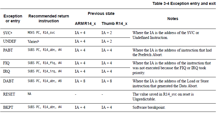
The instruction that caused the data abort is at R14_ABT – 8 which means that the pointer points two instructions beyond the instruction that caused the abort.
The processor takes the prefetch abort if it tries to execute an instruction form a protected or faulty memory location. All prefetch aborts are synchronous.
The instruction that caused the data abort is at R14_ABT – 4. lr_ABT points to the instruction following the one that caused the exception. The handler must return to lr_ABT – 4
The processor takes the undefined instruction exception when it encounters an instruction that is undefined in the appropriate version of the ARM instruction set, or which is for the VFP when the VFP is disabled. The undefined instruction exception can be used to emulate undefined instructions, or simply to handle fault situations.
The instruction that caused the UNDEF abort is at R14_UND – 4.
Why are the return addresses of prefetch abort and data abort different?
For prefetch, the return address is: R14_abt = address of the aborted instruction + 4, and for data abort, the return address is: R14_abt = address of the aborted instruction + 8.
The CPU program counter (PC) is updated at specific points during execution. Exceptions can occur during different phases of fetching/decoding/execution.
In the case of the prefetch abort, the exception occurs only when the processor actually attempts to execute the instruction. The program counter is not updated at the time the prefetch abort is issued, lr_ABT points to the instruction following the one that caused the exception.
In the case of the data abort, the instruction is being executed, and the instruction’s execution causes the exception. When a load or store instruction tries to access memory, the program counter has been updated. A stored value of (pc – 4) in lr_ABT points to the second instruction beyond the address where the exception was generated.
Please refer to Table 3-4 from ARM TRM. This table summarizes the PC value preserved in the relevant R14 on exception entry, and the instruction ARM recommends for exiting the exception handler.
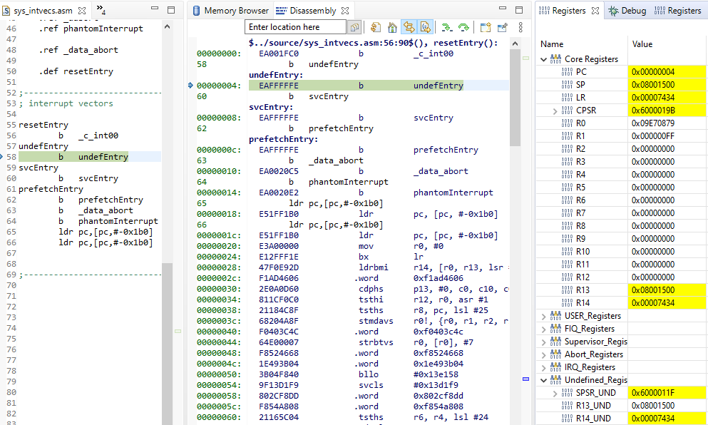
How do I know there is an abort?
When an abort happens, the program gets halted at the Exception Vector Table. Program Counter halts at the address 0x0C(PABT), 0x10(DABT), or 0x04 (UNDEF) if a breakpoint is set at the exception vector address.
There are three important ARM Cortex-R4/R5 registers that can be used to confirm the current state of the processor:
CPSR: The CPSR can be used to verify the current mode of the processor. The mode bits of the CPSR register can be used to check if the current mode is Abort.
M[4:0] Mode 10000 User 10001 FIQ 10010 IRQ 10011 Supervisor 10111 Abort 11011 Undefined 11111 System SPSR: The SPSR can be used to check the previous mode just before entering the exception. For example, if the processor moves from System to Abort Mode, SPSR shows the mode as “System” while CPSR shows the mode as “Abort”. The bit definitions of SPSR register are the same as that of the CPSR register.
R14 Register: The R14 register is used to find the actual instruction or function call that caused the synchronous abort. The actual address of the instruction that triggered the Exception will be R14 - x, where “x” depends on the type of exception.
For details, see Table 3.4, “Exception Entry and Exit” in the Cortex-R4/R5 TRM: https://developer.arm.com/documentation/ddi0363/e/
Undefined Instruction Exceptions (UNDEF)
Undefined instruction exception can occur if the CPU does not understand the fetched instruction.
There are no Fault Status and Fault address registers associated with this exception; only Link register (R14_UND) provides relevant information. The instruction that caused the UNDEF abort is at R14_UND – 4.
7.1 Possible reasons for the execution of a faulty instruction
- Branch to RAM code that has been corrupted or not yet initialized with required functions
- Return address on the stack has been corrupted (for example, stack overflow or pop/push count mismatch).
- Function pointer is not initialized or corrupted.
7.2 Handling Undefined Instruction Exception
- Confirm whether the CPU control is stuck in an Undefined Instruction exception by checking the halt address. If the address is 0x04, then the control has ended in an Undefined Instruction Exception.
- Check the value of the R14_UND register. R14_UND – X provides the address of the instruction which caused the undefined instruction exception. “X” depends on the mode (X=4 for ARM mode, and X=2 for Thumb mode).
- Check the instruction at the address read from R14_UND - X.
- If it is a valid instruction, check whether the mode used (ARM or THUMB) for execution is correct (A mode mismatch for a valid instruction can cause undefined instruction exception).
- If the instruction is invalid, check for address corruption or RAM corruption.
7.3 Example:
When the VFP is not enabled, the processor takes the Undefined Instruction exception when performing a floating operation. CPSR[4:0]=b11011.
The instruction that causes the UNDEF exception is vldr s0, [r13, 0xc] at 0x00007430.
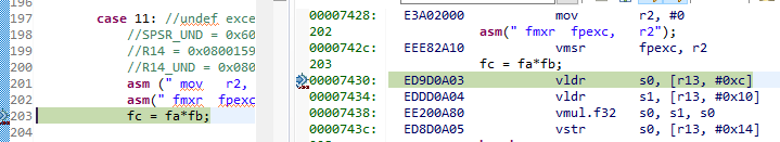
The r14_UND = 0x00007434. The mode before entering UNDEF abort is SPSR_UND[4:0]=b11111 (system mode).
Data Abort Exception (DABT)
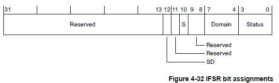
A Data Abort Exception is a response of an invalid data access. If the exception is confirmed to be a Data Abort, as the first step, check the value of the Data Fault Status Register (DFSR) of the Cortex-R CPU.
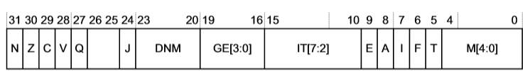
DFSR Register The Figure bellow shows the DFSR register bit assignments:

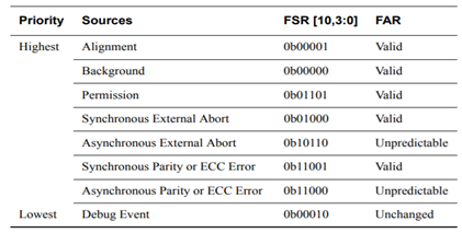
Use the “S” Bit [10] and “Status Bits” [0:3] to understand the nature of the Data Abort. See Table below for status description:
SD Bit
The SD Bit distinguishes between an AXI Decode or Slave error on an external abort. This bit is valid only for external aborts. For all other types of abort, this bit is set to zero:
0 = AXI Decode error (DECERR) or AHB error caused the abort
1 = AXI Slave error (SLVERR) or unsupported exclusive access caused the abort. Example: exclusive access using the AHB peripheral port
RW Bit
The RW bit indicates whether a read or write access caused the abort.
0 = read access caused the abort
1 = write access caused the abort
Common Types of Data Abort
9.1 Background: Memory Protection Unit (MPU) settings must be correct for any region that the CPU is going to access. If the address that the CPU issues falls outside any of the defined regions and the MPU is enabled, the MPU is hard-wired to abort the access. That is, all accesses for an address that is not mapped to a region in the MPU generate a background fault.
A background fault does not occur if the background region is enabled and the access is Privileged. An MPU
background fault might indicate a stack overflow, and be rectified by allocating more stack.
9.2 Permission: This can happen when MPU settings prevent the access of a region. For example, if a User mode application attempts to access a Privileged mode access only region a permission fault occurs.
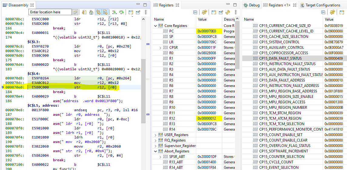
Example:
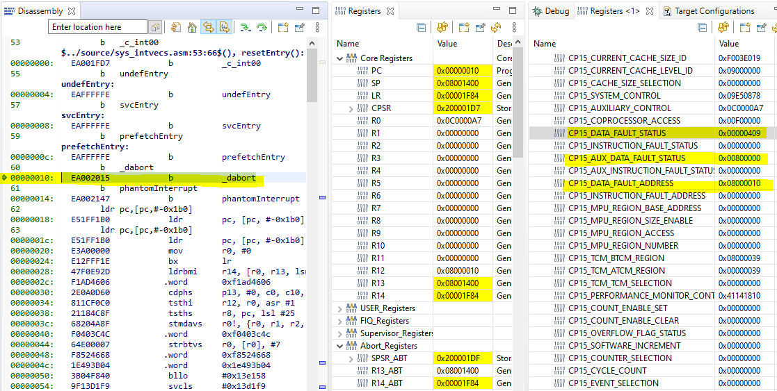
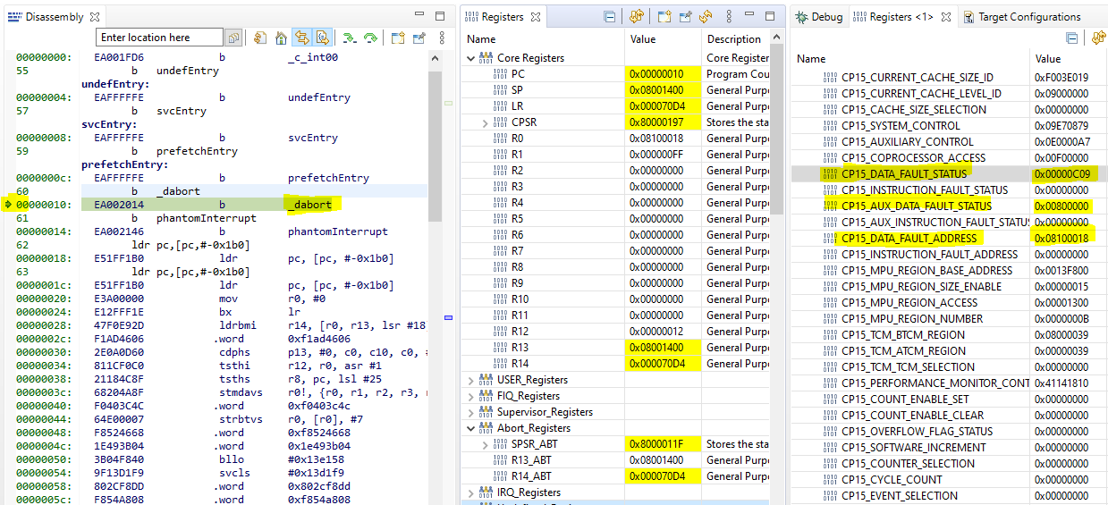
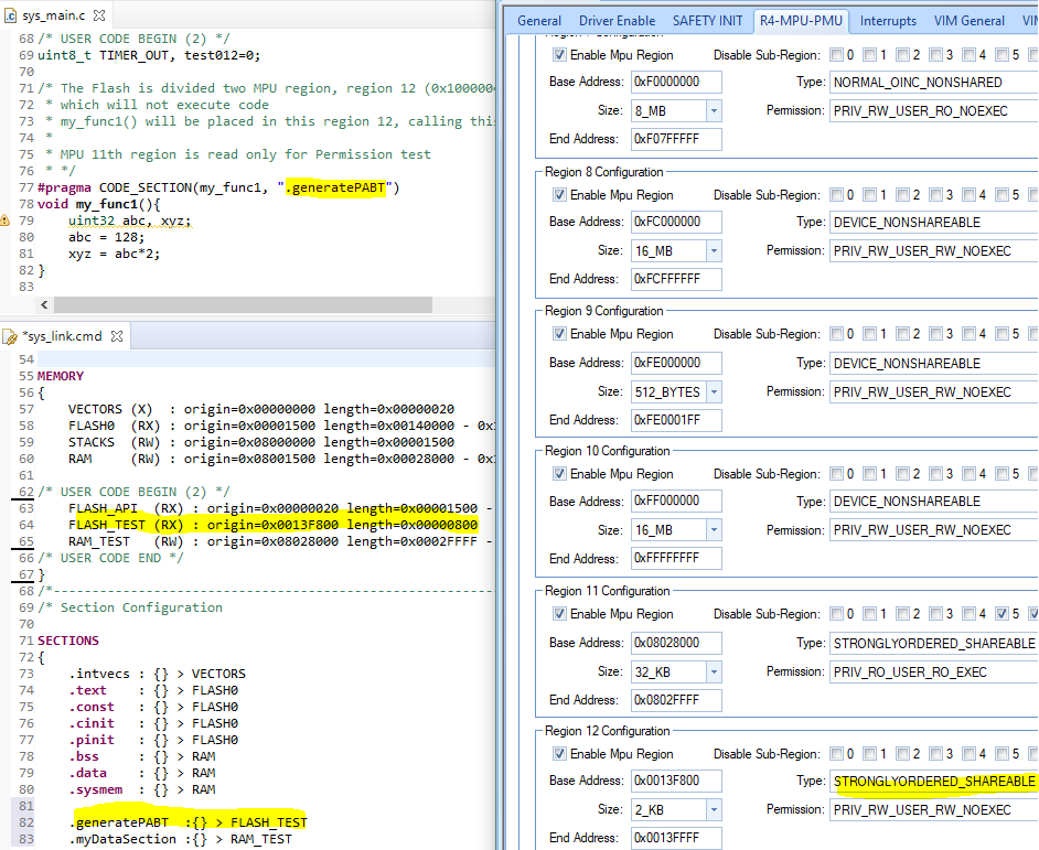
A write operation shown below triggered the abort. The MPU setting for memory location at 0x08028008 is read only.
As shown in Figure below, the DFAR register shows the address that triggered the Data Abort because it is a Permission Error (verified using DFSR) at BTCM (verified using ADFSR). R14_abt – 8 (0x000070E0) points to the instruction that caused that access. It shows a STR operation.
Instructions cannot be executed from regions with Device or Strongly-Ordered memory type attributes.
9.3 Synchronous/Asynchronous External: This happens when the access has been transferred from the CPU to the AXI/AHB Bus and encountered an error. This is the most common fault type that happens with Data Abort. If the Abort is Synchronous, you can check the actual memory address that when accessed resulted in Data Abort using Data Fault Address Register (DFAR), which holds the address of the fault when a synchronous abort occurred.
9.4 Synchronous/Asynchronous ECC: This happens if an ECC error is detected at TCM interfaces or in the cache.
- Examples of Data Abort Exception
10.1 Synchronous abort exceptions
In general, “load” instructions from areas or “store” instructions to memory causing an error are synchronous. DFAR shows the target address of the access. Also, as described in the previous section, R14_abt – 8 points to the instruction that caused that access.
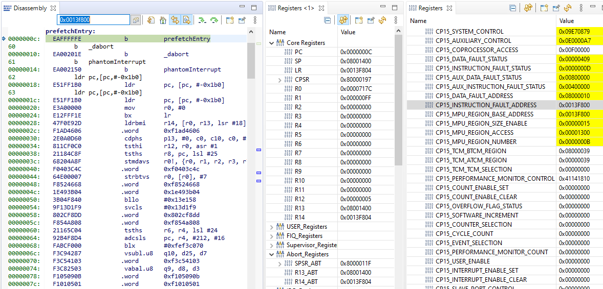
Example 1: Load data from memory location with 2-bit ECC error
A read operation shown below triggered the abort. The data at 0x08000010 has 2-bit ECC error.

As shown in Figure above, the DFAR register shows the address that triggered the Data Abort because it is a Synchronous ECC Error (verified using DFSR) at BTCM (verified using ADFSR). R14_abt – 8 (0x00001F7C) points to the instruction that caused that access. It shows a LDM operation.
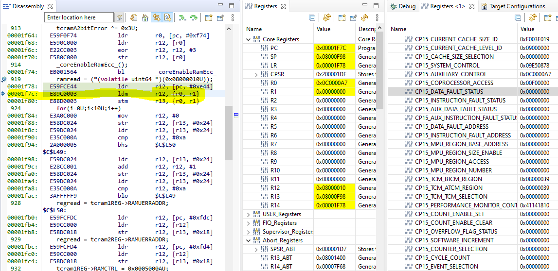
Example 2: Write data to unimplemented memory location
A write operation shown below triggered the abort. The address 0x08100018 is outside the valid memory range.

As shown in Figure above, the DFAR register shows the address that triggered the Data Abort because it is a Synchronous Abort (verified using DFSR). R14_abt – 8 (0x000070CC)points to the instruction that caused that access. It shows an STR operation.
Figure: Before Data Abort Happens
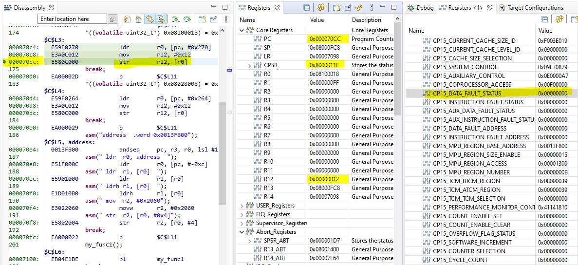
Figure: After Data Abort Happened
10.2 Asynchronous faults
Asynchronous fault is difficult to analyze because we are not able to trace the exact location that resulted in the abort. We cannot use the DFAR register which is used in Synchronous Faults. In general, “store” instructions to areas with “Normal” or “Device” memory attributes causing an error are asynchronous.
From the DFSR Register, we can check status bits, SD bit, and RW bit. SD: Internal AXI decode error, or external AXI slave error RW: Indicates whether a read or write access caused an abort Please read section 8 above for details.
10.3 How to track instruction that caused the asynchronous data abort
- R14_abt – 8 is a location near the instruction that caused the exception.
- Find a “store” instruction near R14_abt – 8, which can likely cause the exception.
- Data Aborts due to issues with MPU
You should define valid MPU settings for the regions accessed in the application so that CPU can access that region accordingly. If you do not define the MPU of a used region, it can cause a Background Fault Data Abort Exception depending on whether privileged access or non-privileged access is used:
11.1 For privileged accesses:
If the BR bit (Bit 17 of the SCTLR Arm register) is set, the default memory map serves as the background region for any access that does not hit a specified region; if the BR bit is 0, a Background Fault exception occurs for any access outside specified regions.
11.2 For non-privileged accesses:
A Background Fault exception occurs for any access outside specified MPU regions. To prevent a Background Fault exception for such accesses, define Region 0 as a Background region covering the entire memory map, which will then be used as the background region for regions outside defined MPUs.
- Prefetch Abort Exception
Prefetch Abort (PABT) Exception occurs when an instruction fetch causes an error. When a Prefetch Abort occurs, the processor marks the prefetched instruction as invalid, but does not take the exception until the instruction is to be executed. If the instruction is not executed, for example because a branch occurs while it is in the pipeline, an abort does not occur. All prefetch aborts are synchronous.
The difference between Undefined Instruction Abort and Prefetch Abort exception is that in case of prefetch, CPU is unable to fetch the instruction from the address; in an Undefined Instruction Exception, the CPU does not know what the instruction does.
The reason for Prefetch Abort can be analyzed by reading the Instruction Fault Status Register (IFSR), the Instruction Fault Address Register (IFAR), and the Auxiliary Instruction Fault Status Register (AIFSR).
IFAR contains the address where the CPU was trying to fetch an instruction from. The contents of IFAR is always valid for a Prefetch Abort, because all Prefetch Aborts are synchronous.
AIFSR record additional information about the nature and location of the fault, for example ATCM (Flash) or BTCM (SRAM).
12.1 Possible reason for prefetch abort
Improper MPU setting: If a permission fault has occurred based on the IFSR status, it is possible that one of the following conditions has occurred:
- An instruction is being fetched from a location for which “Execute Never” attribute is set.
- The target address read from IFAR has “Device” or “Strongly-Ordered” memory attribute. This implicitly means that these areas do not have executable code.
ECC Error on the instruction read:
ECC error is detected on the instruction reads. The IFAR register provides the address that caused the error to be detected. The auxiliary IFSR indicates source of the ECC error.
Wrong return address or branch address - Return address being corrupted - Branch address is corrupted
12.2 Handling Prefetch Abort Exception
Confirm whether the CPU control is stuck in Prefetch Abort Exception by checking the halt address. If the Offset is 0x0C, it indicates that the control has ended in a Prefetch Abort.
Check the status from IFSR and IFAR to determine the type of fault and the address leading to the abort.
In the case of a “permission” fault, find the region in which the address read from the IFAR register falls under. The region can be checked for MPU violations for code area. (Execute Never setting, Device, Strongly-ordered memory).
12.3 Examples of Prefetch Abort Exception
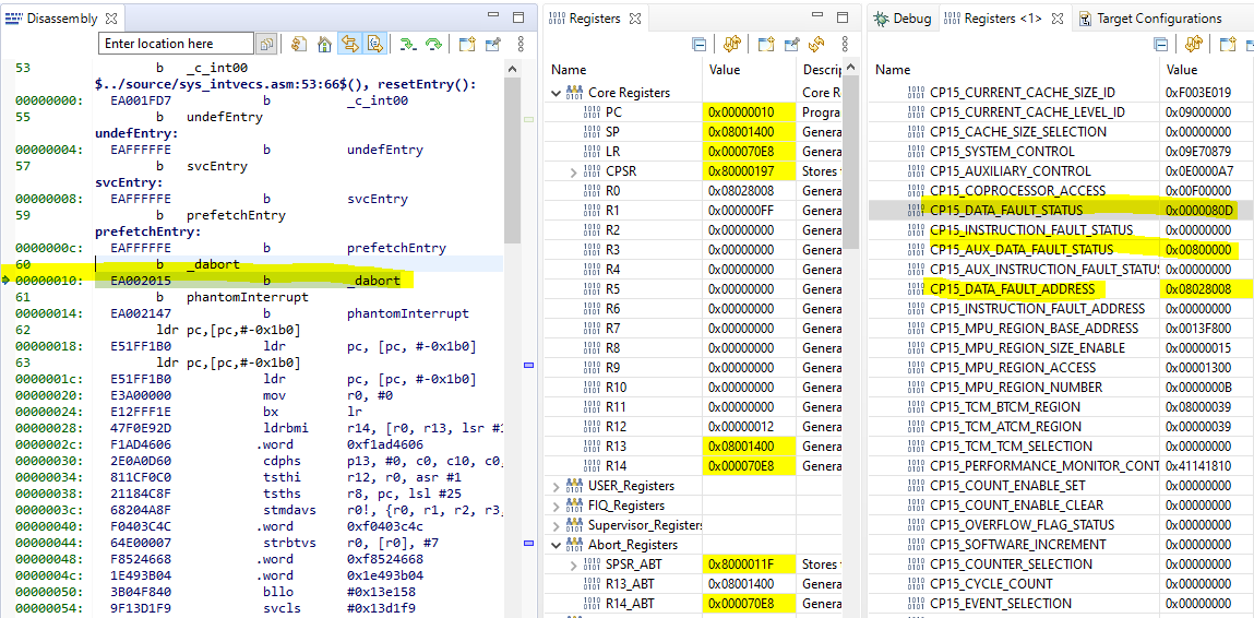
Example 1:
The following example demonstrates the steps to debug a Prefetch Abort. Here, CPU execution was stuck in the Prefetch Abort handler. Relevant register values are as follows:
SPSR_Abt: 0x8000011F: Mode – (11111) System mode. This implies that the CPU was in System mode when the abort was triggered.
IFSR: 0x0000000D:The status indicates a Permission abort. The address captured in IFAR is valid and is the actual address that led to the abort.
IFAR: 0x0013F800:This address falls under a MPU region with strongly-ordered attribute.
Example 2:
Relevant register values for example 2 are as follows:
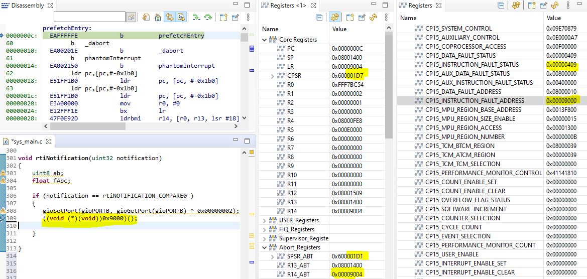
SPSR_Abt: 0x600001D1: Mode – (10001) FIQ mode. This implies that the CPU was in FIQ mode when the abort was triggered.
IFSR: 0x00000409:The status indicates a synchronous external abort or ECC abort. The address captured in IFAR is valid and is the actual address that led to the abort.
IFAR: 0x00009000:This address doesn’t contain a valid instruction and it has wrong ECC value.
AIFSR: 0x00400000: This status indicates that the source of the error is from ATCM (flash).
8.10. DCAN Bus-Off FAQ
What is Can Bus-off state?
Each CAN node has two error counters: the transmit error counter (TEC), and the receive error counter (REC).
A CAN node starts out in Error Active mode. . When TEC or REC exceeds 127, the node becomes
Error-passive. When TEC exceeds the limit of 255, the node enters the Bus-off mode. Upon entering this mode, the error-causing node is forced to shut down and not participate in sending/receiving data on the CAN bus at all.
Is there a way for bus-off node to restore back to normal mode?
The DCAN provides an automatic Auto-Bus-On feature that is enabled by bit ABO in CAN Control Register. If set, the DCAN will automatically start the Bus-Off-Recovery sequence (129 × 11 consecutive recessive bits) after the DCAN has entered Bus-Off state. If ABO is not set, you can start the Bus-Off-Recovery sequence by resetting the init bit in CAN Control Register.
The Bus-Off-Recovery sequence can be delayed by a user-defined number of VCLK cycles that can be defined in Auto-Bus-On Time Register. At the end of the Bus-Off recovery sequence, the error counters will be reset.
However, since bus-off is usually an indication of serious DCAN network errors and may not be fixed by mere automatic recovery sequence, a user-intervened recovery or even a controlled shut-down of the entire system is recommended.
What happens if CANH and CANL are shorted?
The DCAN nodes will enter Bus-Off state. DCAN is a differential protocol. That means 0 or 1 (Dominant and Recessive) is decided on the basis of difference between voltages on CANH and CANL line.
When CANH and CANL is shorted, there will not be any voltage difference and that falls under voltage range of Recessive bits. In other words, Shorting two lines will be considered as continuous transmission of recessive bits.
When transmitting 6 or more consecutive recessive bits, it is considered as Stuffing Error! And when this error count goes more than 255, the controller goes in Bus-Off state.
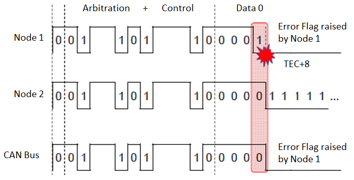
What if two different nodes on the same CAN bus transmit messages with the same ID but different data bytes?
Two nodes on the same network are not allowed to send messages with the same ID. If two nodes try to send a message with the same ID at the same time, arbitration will not work. The node which first transmits a ‘1’ when the other is transmitting a ‘0’ (in data bytes) will get a Bit Error. This node then transmits active error flag,
How to inject bus error to generate DCAN Bus-Off for self-test?
We can induce the bus-off by iteratively injecting attack messages which satisfies the following condition:
- Attacker uses the same message ID of victim node
- The attacker and the Victim node should transmit the messages at the same time
- The attacker’s message should have at least one bit position (in DLC adn Data) in which it is dominant (0), whereas it is recessive (1) in victim’s message.
When the victim and attacker send messages with identical IDs, both nodes win the arbitration. They will send their bit values of control, data, etc on the bus at the same time. Victim sees an opposite polarity on the bus to the one it transmitted. As a result, the victim experiences a bit error (please refer to the picture in prior section) and its TEC increases by 8. By repeating this bus-off attack on the victim’s messages, the attacker can make the victim’s TEC to continuously increase, and force the victim to enter bus-off mode and disconnect from the bus.
What if the CANH is shorted to ground, or CANL is shorted to VCCIO?
As mentioned in #4, the differential signal amplitude is reduced. The communication can not occur between the CAN nodes on the bus.