Note
Additional software examples for Hercules microcontrollers are available on : https://git.ti.com/hercules_examplesThis contains additional software beyond the foundation software components. It includes example boot loader projects, Ethernet-based application demos based on LWIP, application specific software example for Hercules TI designs, as well as basic “getting started” software examples for Hercules Launchpad(s). This will also serve as repository for any software examples and tools that get created in future based on frequently asked questions. To download it: with git, git clone git://git.ti.com/hercules_examples/hercules_examples.git or download one of the compressed file formats under the commit page.
6.1. Project 0
The direct URL for project 0 source code & CCS project is as follows: http://git.ti.com/hercules_examples/hercules_examples/trees/master/Launchpad
The objective of Project 0 is to build a simple example for the purpose of verifying that you have a working development environment. The project itself will do something very simple: Blink an LED.
Currently project 0 is offered on the launchpads of these platforms: RM42L4, RM46L8, RM57L, 570LC43, 570LS04 & 570LS12.
Please refer to Readme.txt for more details to import project into CCS, build, load and run it.
6.2. Project 1
The direct URL for project 1 source code & CCS project is as follows: http://git.ti.com/hercules_examples/hercules_examples/trees/master/Launchpad
The objective of Project 1 is to provide the following demos to highlight some of Hercules MCU’s safety features.
Demo 1: Light Sensor Demo USER LED blinking frequency is controlled by the ambient light sensor. Vary the intensity of the light on the sensor to observe the response.
Demo 2: Force 1 bit Flash ECC error Each press of USER SWITCH A button inserts 1-bit ECC error in flash. Each button press doubles the blink rate of USER LED A (LED2).
Demo 3: Force 2 bit Flash ECC error: Each press of USER SWITCH B button inserts 2-bit ECC error in flash. nERROR lights up when fault is detected. Press USER SWITCH A button to clear nERROR LED.
Demo 4: OSCILLATOR FAILURE OSCILLATOR FAILURE: oscillator can be killed placing jumper JP1 in OSC KILL position to create an oscillator fault which in turn creates error in system. ERR LED is ON as a result. Press nPORRT button (S1) to restore.
Currently project 1 is offered on the launchpads of these platforms: RM42L4, RM46L8, RM57L, 570LC43, 570LS04 & 570LS12.
Please refer to Readme.txt for more details to import project into CCS, build, load and run it.
6.3. Bootloader
The direct URL for MCU safety bootloader source code and CCS project is here: http://git.ti.com/hercules_examples/hercules_examples/trees/master/Bootloaders
The Safety MCU bootloader suppports LC43x, LS31x, LS12x, LS07x, LS04x, RM42, RM44, RM46, RM48, and RM57 families, supports the latest F021 Flash API V2.01.01, and uses the HALCoGen 4.07.01 generated drivers for device and peripherals’ initialization. The bootloader and application are tested on TI HDKs.
6.3.1. New features
- Supports F021 Flash API 2.01.01
- Generates flash ECC using Linker CMD file to avoid speculative fetch ECC error.
- TMS570LC43x, RM57Lx, TMS570LS07x and RM44Lx devices are supported
- Changed APPLICATION START ADDRESS to 0x10020, The 0x10000~0x10020 is left for application update status, code rev number(.30.00), and year (2019).
- Copy the const (used by flash erase/program functions)to SRAM
- Use HALCoGen driver for initialization
- Separate flash bank/sector initialization and activiation from flash erase/program functions. It is called only one time.
Please refer to Readme.txt for more details.
6.4. lightweight IP (lwIP) demo
The direct URL for source code & CCS project is as follows: http://git.ti.com/hercules_examples/hercules_examples/trees/master/Application/LwIP
The demo illustrates the use of integration of Ethernet driver and lightweight IP (lwIP), which is a widely used open-source TCP/IP stack designed for embedded systems. The demo runs a static webserver. The driver code is generated with TI HALCoGen, and lwIP is ported to the Hercules devices.
The project is supported for the following platforms: RM46x HDK, RM48x HDK, RM57x HDK, TMS570LS12x HDK, TMS570LS31x HDK, TMS570LC43x HDK, LAUNCHXL2-RM57x and LAUNCHXL2-TMS570LC43x.
Please refer to User Guide under docs for more details. Also, an application report: HALCoGen Ethernet Driver With lwIP Integration Demo and Active Web Server Demo is available for further reading.
6.5. active webserver demo
The direct URL for source code & CCS project is as follows: http://git.ti.com/hercules_examples/hercules_examples/trees/master/Application/ActiveWebserver
The active webserver demo extends the lwIP demo. It serves a web page which can be navigated, and it also allows to control some LEDs on the launchpad. There are two demos bundled, show cases the CGI and SSI CGI handling capability of the webserver
The project is supported for the following platforms: LAUNCHXL2-RM57x and LAUNCHXL2-TMS570LC43x.
Please refer to readme under docs for more details. Also, an application report: HALCoGen Ethernet Driver With lwIP Integration Demo and Active Web Server Demo is available for further reading.
6.6. Using DMA to transfer data in SPI compatibility mode
The direct URL for SPI DMA source code & CCS project is as follows:
http://git.ti.com/hercules_examples/hercules_examples/trees/master/application/TMS570_SPI_DMA
The objective of SPI DMA is to build a simple example to demostrate the configurations of SPI and DMA Please refer to Readme.txt for more details to import project into CCS, build, load and run it.
Introduction
Serial peripheral interface (SPI) is one of the most widely used interfaces between microcontroller and peripheral ICs such as shift registers, sensors, ADCs, SRAM, SD Card, and others. SPI is a synchronous, full duplex master-slave-based interface. The data from the master or the slave is synchronized on the rising or falling clock edge. Both master and slave can transmit data at the same time. The SPI interface can be 3-wire, 4-wire, or 5-wires. This example uses the popular 4-wire SPI interface.
The DMA controller is used to transfer data between two locations in the memory map in the background of CPU operations. This application report demonstrates how to use the DMA to free CPU cycles while transmitting SPI messages. The example was designed to be run on the LAUNCHXL2 series of launchpads.
Basic Steps to Setup a DMA SPI Transfer
In order to use the DMA for data transfer between the SPI and the device data RAM, the module needs to be setup properly. The following bullets show the basic steps that need to be performed to do this.
- Initialize the desired SPI (example uses SPI3 and SPI5)
- Enable DMA
- Enable DMA Interrupt
- Assign SPI DMA request to DMA channel
- Configure the DMA control packets for RX and TX
- Enable SPI DMA request
- Trigger DMA transfers
- Get transfer ready notification
Use DMA in Standard SPI Mode
The SPI allows a serial bit stream of programmed length (two to 16 bits) to be shifted into and out of the device at a programmed bit-transfer rate. 16 bits of data word length (CHARLEN) is used in this example.
In order to reduce CPU overhead in handling SPI message traffic on a character-by-character basis, SPI can use the DMA controller to transfer the data.
For transmitting, the DMA reads 16 bits at a time from the data RAM incrementing the address, writing 16 bits of data to SPI transmit data register (SPIDAT1) without incrementing the address.
For receiving, the DMA reads 16 bits of data from SPI receive buffer (SPIBUF) without incrementing the source address, and writing the data to the data RAM incrementing the address.
The SPI transmits one word at a time until the entire message has been sent and sets a complete flag in the data RAM for the CPU to know when it is ready to send another message.
DMA port used for data transfer
For Cortex-R5F devices (RM57Lx, and TMS570LC43x), there are two DMA ports (Port A and Port B). Flash, SRAM and EMIF are mapped to Port A, and all peripherals and their memories are mapped to Port B. To transfer received data from SPIBUF register to SRAM, write 0x0 (Port B read, Port A write ) to the respective channels in the PARx registers. To transfer data from SRAM to SPIDAT1 register, write 0x1 (Port A read, Port B write ) to the respective channels in the PARx registers.
g_dmaCTRLPKT_RX.PORTASGN = PORTB_READ_PORTA_WRITE;
g_dmaCTRLPKT_TX.PORTASGN = PORTA_READ_PORTB_WRITE;
For Cortex-R4F device (RM4x, and TMS570LSx), there is only one DMA port (Port B). DMA data read and write access happens through Port B. Write 0x4 to the respective channels in the PARx registers for both transfers (from SPIBUF to SRAM, and from SRAM to SPIDAT1).
g_dmaCTRLPKT_RX.PORTASGN = 4;
g_dmaCTRLPKT_TX.PORTASGN = 4;
SPI DMA Request Generation
The DMA request enable bit (DMAREQEN in SPIINT0 register) controls the assertion of requests to the DMA controller module.
When a character is being transmitted or received, the SPI will signal the DMA via the DMA request signals, TX_DMA_REQ and RX_DMA_REQ. The DMA controller will then perform the required data transfer.
The SPI generates a request on the TX_DMA_REQ line each time the TX data is copied to the TX shift register either from the TXBUF or from SPIDAT1 (when TXBUF is empty).
The SPI generates a request on the RX_DMA_REQ line each time the received data is copied to the SPIBUF.
The first TX_DMA_REQ pulse is generated when DMAREQEN (SPIINT0[16]) and SPIEN (SPIGCR1[24]) are set to 1.
spiREG3->GCR1 |= (0x1 << 24);
spiREG3->INT0 |= (0x1 << 16);
SPI DMA Request Assignment
Cortex-R4F devices (RM4x, and TMS570LSx) have 16 DMA channels and up to 32 peripheral hardware DMA requests. DMA request #30 (DMAREQ[30]) is used for SPI5 receive DMA in standard SPI mode, and DMA request #15 (DMAREQ[15]) is used for SPI3 transmit DMA in standard SPI mode (refer to Table 6-33 in Datasheet).
Cortex-R5F devices (RM4x, and TMS570LSx) have 32 DMA channels and up to 48 peripheral hardware DMA requests. DMA request #30 (DMAREQ[30]) is used for SPI5 receive DMA in standard SPI mode, and DMA request #15 (DMAREQ[15]) is used for SPI3 transmit DMA in standard SPI mode (refer to Table 6-41 in Datasheet).
Some DMA requests have multiple sources, you must ensure that only one of these DMA request sources is enabled at any time.
dmaReqAssign(DMA_CH0, 30);
dmaReqAssign(DMA_CH1, 15);
DMA channel for transmit and receive
The control packer is mapped to DMA channel in fixed number order. For example, the control packet 0 stores channel information for channel 0. Any DMA channel can be used for SPI transfer. The example uses DMA channel 0 for receiving data and channel 1 for transmitting data.
dmaSetCtrlPacket(DMA_CH1, g_dmaCTRLPKT_TX);
dmaSetCtrlPacket(DMA_CH0, g_dmaCTRLPKT_RX);
Address to access the SPI registers
For transmitting, the DMA writes data to TXDATA (SPIDAT1[15:0]). For receiving, the DMA reads data from RXDATA (SPIBUF[15:0]). For big endian devices (TMS570Lx), the address of RXDATA and TXDATA is the base address plus 2 (CHARLEN=16), or plus 3 (CHARLEN=8).
#if ((__little_endian_\_ == 1) \|\| (__LITTLE_ENDIAN_\_ == 1))
   #define SPI3_TX_ADDR ((uint32_t)(&(spiREG3->DAT1)) + 0)
   #define SPI5_RX_ADDR ((uint32_t)(&(spiREG5->BUF)) + 0)
#else
   #define SPI3_TX_ADDR ((uint32_t)(&(spiREG3->DAT1)) + 2)
   #define SPI5_RX_ADDR ((uint32_t)(&(spiREG5->BUF)) + 2)
#endif
Example: configuration of DMA channel control packets:
void dmaConfigCtrlRxPacket (uint32 sadd, uint32 dadd, uint16 ElmntCnt, uint16 FrameCnt)
{
    g_dmaCTRLPKT_RX.SADD = sadd;
    g_dmaCTRLPKT_RX.DADD = dadd;
    g_dmaCTRLPKT_RX.CHCTRL = 0;
    g_dmaCTRLPKT_RX.FRCNT = FrameCnt;
    g_dmaCTRLPKT_RX.ELCNT = ElmntCnt;
    g_dmaCTRLPKT_RX.ELDOFFSET = 0;
    g_dmaCTRLPKT_RX.ELSOFFSET = 0;
    g_dmaCTRLPKT_RX.FRDOFFSET = 0;
    g_dmaCTRLPKT_RX.FRSOFFSET = 0;
    g_dmaCTRLPKT_RX.PORTASGN = 4;
    g_dmaCTRLPKT_RX.RDSIZE = ACCESS_16_BIT;
    g_dmaCTRLPKT_RX.WRSIZE = ACCESS_16_BIT;
    g_dmaCTRLPKT_RX.TTYPE = FRAME_TRANSFER;
    g_dmaCTRLPKT_RX.ADDMODERD = ADDR_FIXED;
    g_dmaCTRLPKT_RX.ADDMODEWR = ADDR_INC1;
    g_dmaCTRLPKT_RX.AUTOINIT = AUTOINIT_ON;
}

void dmaConfigCtrlTxPacket (uint32 sadd, uint32 dadd, uint16 ElmntCnt, uint16 FrameCnt)
{
    g_dmaCTRLPKT_TX.SADD = sadd;
    g_dmaCTRLPKT_TX.DADD = dadd;
    g_dmaCTRLPKT_TX.CHCTRL = 0;
    g_dmaCTRLPKT_TX.FRCNT = FrameCnt;
    g_dmaCTRLPKT_TX.ELCNT = ElmntCnt;
    g_dmaCTRLPKT_TX.ELDOFFSET = 0;
    g_dmaCTRLPKT_TX.ELSOFFSET = 0;
    g_dmaCTRLPKT_TX.FRDOFFSET = 0;
    g_dmaCTRLPKT_TX.FRSOFFSET = 0;
    g_dmaCTRLPKT_TX.PORTASGN = 4;
    g_dmaCTRLPKT_TX.RDSIZE = ACCESS_16_BIT;
    g_dmaCTRLPKT_TX.WRSIZE = ACCESS_16_BIT;
    g_dmaCTRLPKT_TX.TTYPE = FRAME_TRANSFER;
    g_dmaCTRLPKT_TX.ADDMODERD = ADDR_INC1;
    g_dmaCTRLPKT_TX.ADDMODEWR = ADDR_FIXED;
    g_dmaCTRLPKT_TX.AUTOINIT = AUTOINIT_ON;
}
6.7. Using Performance Monitoring Unit (PMU) to evaluate code efficiency
Instruction The ARM Cortex-R4/5 includes logic to detect various events that can occur. These events provide useful information about the behavior of the processor that you can use when debugging code. The events are visible on an output event bus, and can be counted by event counters in the Performance Monitoring Unit (PMU).
The ARM Cortex-R4/5 PMU consists of one cycle counting register, three event counting registers, and 12 CP15 registers for controlling and interrogating the counters. The PMU registers are always accessible in Privileged mode. We can configure User Enable register (PMUSERENR) to make PMU registers (except for PMINTENSE, and PMINTENCLR) to be accessible in User mode.
This example outlines the steps required to setup and use of PMU registers and counters for measuring the code execution time, execution cycles per instruction, and D/I cache miss rate. The example also shows the different execution time between un-optimized function and optimized function.
Source code performing this demo can be found in following link:
http://git.ti.com/hercules_examples/hercules_examples/trees/master/Application/TMS570LC43x_PMU_Demo
Using PMU Cycle Counter to measure the code execution time
Hercules MCUs support multiple methods to measure the code execution time: pin toggle, RTI cycle count, and PMU cycle count. The best is to use PMU counter:
- The PMU has minimal overhead. The PMU registers (unlike the RTI) are in the coprocessor space, rather than memory mapped. It takes only 6 cycles to copy the PMU register to a working registers.
- The PMU can count CPU clock cycles during the time the measured code is running. It has better resolution than the RTI cycle count method which counts RTI clock cycles.
2.1 Setting up and using the Cycle counter
This section outlines the steps required to setup and use the cycle counter on a Cortex-R4/5.
Enabling the PMU - in the Performance Monitors Control Register (PMCR), set the E,bit[0] to 1.
_pmuInit_();Enabling PMU user access (no essential) - in the Performance Monitors User Enable Register (PMUSERENR), set the EN, bit[0] to 1.
_pmuEnableUserMode_();Enabling the cycle counter (CCNT) - in the Performance Monitors Count Enable Set Register (PMCNTENSET), set the C,bit[31] to 1.
_pmuEnableCountersGlobal_();Resetting the cycle counter (CCNT) - in the Performance Monitors Control Register (PMCR), set the C,bit[2] to 1.
_pmuResetCycleCounter_()Start the cycle counter (CCNT) - in the Performance Monitors Control Enable Set Register (PMCNTENSET), set bit[31] to 1.
_pmuStartCounters_( pmuCYCLE_COUNTER);Code Section to be measured: add_matrix();
Stop the cycle counter (CCNT) - in the Performance Monitors Count Enable Clear Register (PMCNTENCLR), set the C,bit[31] to 1.
_pmuStopCounters_(pmuCYCLE_COUNTER);Reading the value of the cycle counter (CCNT) - the value of the cycle counter is stored in the Performance Monitors Cycle Count Register (PMCCNTR).
cycles = _pmuGetCycleCount_();
2.1 Comparison between un-optimized code and local optimized code
The file which contains the matrix addition function is local optimized using TI ARM compiler.
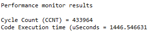
Un-optimized code takes 1446 cycles:
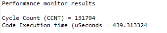
Optimized code takes only 439 cycles:
Using PMU Counter to measure the execution cycles per instruction
The PMU uses event numbers to identify events. The PMU on Cortex-R4/5 has three event counters, and each event counter can only monitors a single event at a time. Event counters provide highly accurate information, and using event counters is a non-invasive debug feature with minimal impact on performance.
This section is to use event counters to measure the total number of clock cycles and the number of instructions executed, from which a cycles per instruction figure can be derived. This can be a good indicator of the core’s efficiency in a particular section of code.
3.1 Setting up and using the event counters
This section outlines the steps required to setup and use the event counters.
Enabling the PMU - in the Performance Monitors Control Register (PMCR), set the E,bit[0] to 1.
_pmuInit_();Enabling PMU user access (no essential) - in the Performance Monitors User Enable Register (PMUSERENR), set the EN, bit[0] to 1.
_pmuEnableUserMode_();Enabling the cycle counter (CCNT) and Event Counters - in the Performance Monitors Count Enable Set Register (PMCNTENSET), set the C,bit[31] to 1.
_pmuEnableCountersGlobal_();Configuring event counters - In the Performance Monitors Event Counter Selection Register (PMSELR), write the counter number (0-5) to the SEL,bits[4:0] you wish to configure.
In the Performance Monitors Event Type Select Register (PMXEVTYPER), write the event number (from the event list) to evtCount,bits[7;0], in order to select the event being monitored by the counter
_pmuSetCountEvent_(pmuCOUNTER0, PMU_INST_ARCH_EXECUTED);
_pmuSetCountEvent_(pmuCOUNTER1, PMU_DATA_READ_ARCH_EXECUTED);
_pmuSetCountEvent_(pmuCOUNTER2, PMU_DATA_WRITE_ARCH_EXECUTED);
Resetting the cycle counter (CCNT) and Event counters - in the Performance Monitors Control Register (PMCR), the C and P, bit[3] and bit[2] to 1.
_pmuResetCounters_();Start the cycle counter (CCNT) and Event counters - in the Performance Monitors Control Enable Set Register (PMCNTENSET), set bit[31] and bit[2:1] to 1.
_pmuStartCounters_(pmuCYCLE_COUNTER|pmuCOUNTER0|pmuCOUNTER1|pmuCOUNTER2);Code Section to be measured: add_matrix();
Stop the cycle counter (CCNT) and Event Counters - in the Performance Monitors Count Enable Clear Register (PMCNTENCLR), set the bit[31] and bit[2:0] to 1.
_pmuStopCounters_(pmuCYCLE_COUNTER|pmuCOUNTER0|pmuCOUNTER1|pmuCOUNTER2);Reading the value of the cycle counter (CCNT) and Event counters - the value of the cycle counter is stored in the Performance Monitors Cycle Count Register (PMCCNTR) and Event Count Registers (PMXEVCNTR[2:0]).
cycles = _pmuGetCycleCount_();
event0_cycles = _pmuGetEventCount_(pmuCOUNTER0);
event1_cycles = _pmuGetEventCount_(pmuCOUNTER1);
event2_cycles = _pmuGetEventCount_(pmuCOUNTER2);
Calculating the cycles per instruction
cycl_inst = (float)cycles / (float)event0_cycles;
3.2 Comparison between un-optimized code and local optimized code
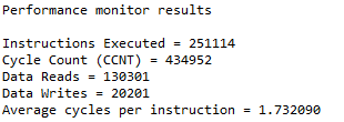
The file which contains the matrix addition function is local optimized using TI ARM compiler. Un-optimized code, one instruction takes 1.73 cycles:
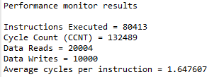
Optimized code, one instruction takes 1.65 cycles. The optimized code has much less instructions for this matrix addition.
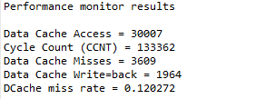
Using PMU Counter to measure D-Cache Miss Rate
This section is to use event counters to measure the total number of L1 D-Cache refills and L1 D-Cache accesses, which are used to determine the ratio of L1 D-Cache misses to L1 D-Cache accesses. This provides an indication of how efficiently the cache is being used and can potentially explain excessive data accesses to the external memory system that are slowing down your program.
4.1 Setting up and using the event counters
This section outlines the steps required to setup and use the event counters.
Enabling the PMU - in the Performance Monitors Control Register (PMCR), set the E,bit[0] to 1.
_pmuInit_();Enabling PMU user access (no essential) - in the Performance Monitors User Enable Register (PMUSERENR), set the EN, bit[0] to 1.
_pmuEnableUserMode_();Enabling the cycle counter (CCNT) and Event Counters - in the Performance Monitors Count Enable Set Register (PMCNTENSET), set the C,bit[31] to 1.
_pmuEnableCountersGlobal_();Configuring event counters - In the Performance Monitors Event Counter Selection Register (PMSELR), write the counter number (0-5) to the SEL,bits[4:0] you wish to configure.
In the Performance Monitors Event Type Select Register (PMXEVTYPER), write the event number (from the event list) to evtCount,bits[7;0], in order to select the event being monitored by the counter.
_pmuSetCountEvent_(pmuCOUNTER0, PMU_DATA_CACHE_ACCESS );
_pmuSetCountEvent_(pmuCOUNTER1, PMU_DATA_CACHE_MISS );
_pmuSetCountEvent_(pmuCOUNTER2, PMU_DATA_CACHE_WRITE_BACK );
Resetting the cycle counter (CCNT) and Event counters - in the Performance Monitors Control Register (PMCR), the C and P, bit[3] and bit[2] to 1.
_pmuResetCounters_();Start the cycle counter (CCNT) and Event counters - in the Performance Monitors Control Enable Set Register (PMCNTENSET), set bit[31] and bit[2:1] to 1.
_pmuStartCounters_(pmuCYCLE_COUNTER|pmuCOUNTER0|pmuCOUNTER1|pmuCOUNTER2);Code Section to be measured: add_matrix();
Stop the cycle counter (CCNT) and Event Counters - in the Performance Monitors Count Enable Clear Register (PMCNTENCLR), set the bit[31] and bit[2:0] to 1.
_pmuStopCounters_(pmuCYCLE_COUNTER|pmuCOUNTER0|pmuCOUNTER1|pmuCOUNTER2);Reading the value of the cycle counter (CCNT) and Event counters - the value of the cycle counter is stored in the Performance Monitors Cycle Count Register (PMCCNTR) and Event Count Registers (PMXEVCNTR[2:0]).
cycles = _pmuGetCycleCount_();*
event0_cycles = _pmuGetEventCount_(pmuCOUNTER0);
event1_cycles = _pmuGetEventCount_(pmuCOUNTER1);
event2_cycles = _pmuGetEventCount_(pmuCOUNTER2);
Calculating the D-cache miss rate:
cache_miss_rate = (float)event1_cycles / (float)event0_cycles;
4.2 Comparison between un-optimized code and local optimized code
The file which contains the matrix addition function is local optimized using TI ARM compiler. Un-optimized code, one instruction takes 1.73 cycles:
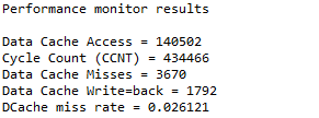
Optimized code, D-cache miss doesn’t have change, but the cache accesses and cycle count decrease a lot.
Using PMU Counter to measure I-Cache Miss Rate
This section is to use event counters to measure the total number of L1 I-Cache refills and L1 I-Cache accesses, which are used to determine the ratio of L1 I-Cache misses to L1 I-Cache accesses. This provides an indication of how efficiently the cache is being used and can potentially explain excessive data accesses to the external memory system that are slowing down your program.
The ratio of cache-misses to instructions will give an indication how well the cache is working; the lower the ratio the better.
5.1 Setting up and using the event counters
This section outlines the steps required to setup and use the event counters.
Enabling the PMU - in the Performance Monitors Control Register (PMCR), set the E,bit[0] to 1.
_pmuInit_();Enabling PMU user access (no essential) - in the Performance Monitors User Enable Register (PMUSERENR), set the EN, bit[0] to 1.
_pmuEnableUserMode_();Enabling the cycle counter (CCNT) and Event Counters - in the Performance Monitors Count Enable Set Register (PMCNTENSET), set the C,bit[31] to 1.
_pmuEnableCountersGlobal_();Configuring event counters - In the Performance Monitors Event Counter Selection Register (PMSELR), write the counter number (0-5) to the SEL,bits[4:0] you wish to configure. In the Performance Monitors Event Type Select Register (PMXEVTYPER), write the event number (from the event list) to evtCount,bits[7;0], in order to select the event being monitored by the counter
_pmuSetCountEvent_(pmuCOUNTER0, PMU_INST_CACHE_ACCESS );
_pmuSetCountEvent_(pmuCOUNTER1, PMU_INST_CACHE_MISS );
_pmuSetCountEvent_(pmuCOUNTER2, PMU_INST_ARCH_EXECUTED );
Resetting the cycle counter (CCNT) and Event counters - in the Performance Monitors Control Register (PMCR), the C and P, bit[3] and bit[2] to 1.
_pmuResetCounters_();Start the cycle counter (CCNT) and Event counters - in the Performance Monitors Control Enable Set Register (PMCNTENSET), set bit[31] and bit[2:1] to 1.
_pmuStartCounters_(pmuCYCLE_COUNTER|pmuCOUNTER0|pmuCOUNTER1|pmuCOUNTER2);Code Section to be measured: add_matrix();
Stop the cycle counter (CCNT) and Event Counters - in the Performance Monitors Count Enable Clear Register (PMCNTENCLR), set the bit[31] and bit[2:0] to 1.
_pmuStopCounters_(pmuCYCLE_COUNTER|pmuCOUNTER0|pmuCOUNTER1|pmuCOUNTER2);Reading the value of the cycle counter (CCNT) and Event counters - the value of the cycle counter is stored in the Performance Monitors Cycle Count Register (PMCCNTR) and Event Count Registers (PMXEVCNTR[2:0]).
cycles = _pmuGetCycleCount_();
event0_cycles = _pmuGetEventCount_(pmuCOUNTER0);
event1_cycles = _pmuGetEventCount_(pmuCOUNTER1);
event2_cycles = _pmuGetEventCount_(pmuCOUNTER2);
Calculating the I-cache miss rate:
cache_miss_rate = (float)event1_cycles / (float)event0_cycles;
6.8. Example of Sequence to Enter a Low-Power Mode
The direct URL for source code & CCS project is as follows:
The typical Software Sequence to Enter a Low-Power Mode
Program the flash banks and flash pump fall-back modes to be “sleep”
The flash pump transitions from active to sleep mode only after all the flash banks have switched from active to sleep mode. The flash banks start switching from active to sleep mode only after the banks are not accessed for at least a duration defined by the Active Grace Period (AGP) parameter configured for the banks. See Chapter 5 for more details.
flashWREG->FPAC2 = 0x7;
flashWREG->FMAC = 0x6;
flashWREG->FBAC = 0x70F;
flashWREG->FMAC = 0x0;
flashWREG->FBAC = 0x70F;

 /* Setup flash module to change fallback modes for banks/pump to be "sleep" */
 flashWREG->FBFALLBACK = 0x00000000U
                         | (uint32)((uint32)SYS_SLEEP << 14U) /* BANK 7 */
                         | (uint32)((uint32)SYS_SLEEP << 2U)  /* BANK 1 */
                         | (uint32)((uint32)SYS_SLEEP << 0U); /* BANK 0 */

 /* Disable oscillator monitoring to prevent detection of osc fail */
 systemREG1->CLKTEST = 0x010A0000;
The flash banks/pump are one of the key “gates” to be able to turn the system clock (HCLK) domain off. The flash interface module “allows” the HCLK domain to be turned off only after the flash banks and pump have entered their own “sleep” state. As stated in the above paragraph, the “active grace period” counter starts counting once it detects no flash bank accesses. This is possible only once the CPU clock domain (GCLK) is disabled. So the first step in putting the part into any low-power mode is to disable the GCLK clock domain. Configuring the flash bank and pump “fall back” modes to “sleep” only indicates that they need to enter their individual sleep modes once their AGP counters expire. The actual entry to sleep mode will be initiated once the CPU clock domain gets disabled.
Disable the clock sources that are not required to be kept active
A clock source does not get disabled until all clock domains using that clock source are disabled first, or are configured to use an alternate clock source.
The clock sources that need to be disabled depends on the actual low-power mode that you plan to enter. We have pre-defined the three LPMs (doze, snooze and sleep) depending on which clock sources you could choose to keep active through the low-power state. For example, the main oscillator could be kept active while all other clock sources (PLLs, LPO) could be disabled. This is the doze mode, and allows for a faster wake-up.
/* turn off all clock sources for enterring **SLEEP** Mode*/
systemREG1->CSDISSET = 0xFF;
A clock source can be commanded to be disabled by writing to either the Clock Source Disable (CSDIS) register or setting the correct bit(s) in the CSDISSET register (avoids read-modify-write operation). As part of the safety requirements to be fulfilled, a clock source does not really get disabled until all clock domains using this clock source are either switched over to another clock source or are themselves disabled first. For example, let’s say you want to enter doze mode. So you will set all bits in the CSDISSET register except for bit 0 (for the main oscillator). Now suppose that the GHVSRC register has been configured such that the GCLK/HCLK/VCLK domains are sourced by PLL1. In this case, even if you set the bit 1 of the CSDISSET register (corresponds to PLL1), PLL1 will not get disabled until the GCL/HCLK/VCLK domains are either switched over to another clock source, or are disabled first.
Disable the clock domains that are not required to be kept active
A clock domain does not get disabled until all modules using that clock domain “give their permission” for that clock domain to be turned off.
/* turn off all clock domains for enterring **SLEEP** Mode*/
systemREG1->CDDISSET = 0xFFFF;
This is done by configuring the Clock Domain Disable (CDDIS) register or setting the correct bit(s) in the CDDISSET register (again, to avoid a read-modify-write operation). As explained earlier with respect to the flash interface module holding HCLK active, there are “gates” to be closed before any clock domain can be disabled. Configuring the CDDIS or CDDISSET register only indicates which clock domains need to be disabled once their disabling conditions are met.
Idle the Cortex-R4F core
The ARM Cortex-R4F CPU has internal power management logic, and requires a dedicated instruction to be used in order to enter a low power mode. This is the Wait For Interrupt (WFI) instruction. When a WFI instruction is executed, the Cortex-R4F core flushes its pipeline, flushes all write buffers, and completes all pending bus transactions. At this time the core indicates to the system that the clock to the core can be stopped. This indication is used by the Global Clock Module (GCM) to turn off the CPU clock domain (GCLK) if the CDDIS register bit 0 is set.
asm(" WFI");
asm(" nop");
asm(" nop");
asm(" nop");
This is the main “entry point” into the desired low-power mode. As discussed earlier, this steps allows the CPU clock domain (GCLK) to be disabled. This allows the flash interface module to count down the AGP for the bank/pump and put these macros to sleep. This, in turn, allows HCLK domain (and VCLKx) to be disabled. If you want to enter a low-power mode wherein a clock source is kept active (doze/snooze), then usually you will configure the RTICLK domain to be sourced from this active clock source. In this case, the RTICLK domain is not disabled, but switched over to use the main oscillator or LPO as its source. This allows you to periodically wake up the part using main oscillator + RTI as the time base generator.
Once all clock domains except RTICLK are disabled, all the commanded clock sources will also get disabled (except for the one that is clocking the RTI), and the part is now considered to be in a low-power mode.
6.9. Hercules Motorware 1.00.03.03
The direct URL for source code & CCS project is as follows: http://git.ti.com/hercules_examples/hercules_examples/trees/master/Application/motorware
6.10. TI Design
URL for TI Design source code & CCS projects: http://git.ti.com/hercules_examples/hercules_examples/trees/master/TI_Design
CAN-FD TI Design: https://www.ti.com/tool/TIDEP-01014
This reference design showcases controller area network, flexible data-rate communication (CAN FD) on Hercules™ TMS570 microcontrollers using the TCAN4550 CAN FD controller. The interface between the TMS570 and the TCAN parts is done through a serial peripheral interface (SPI). This example can be used to implement CAN FD communication on any Hercules™ microcontroller that does not natively support CAN FD.